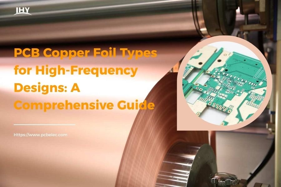
Table of Contents
Why Small Mistakes Break High‑Frequency PCBs
At low frequencies, many layout mistakes only cost you a bit of margin; the circuit still works, just not perfectly. In high‑frequency and RF designs, the same mistakes—poor stackup choices, sloppy routing, weak grounding, or the wrong vias—can completely break the board, even when the schematic and simulations look solid. Tiny discontinuities in impedance, unexpected coupling between traces, or an overlooked via stub can turn into reflections, loss, oscillations, and EMI problems that are hard to debug once the PCB is fabricated.
The good news is that most high‑frequency PCB failures come from a relatively short list of recurring design errors. They show up across different industries and applications because they are rooted in the same physical effects: transmission‑line behavior, parasitics, and how real boards are manufactured. This article walks through the most common high‑frequency PCB design mistakes we see—especially in stackup, placement, routing, grounding, vias, and material selection—and shows concrete ways to avoid them in your next RF board so you are much more likely to get “first‑pass” success instead of an expensive re‑spin.
If you need a manufacturing partner who can actually build and validate these high‑frequency designs, our RF and high‑frequency PCB fabrication services can help.
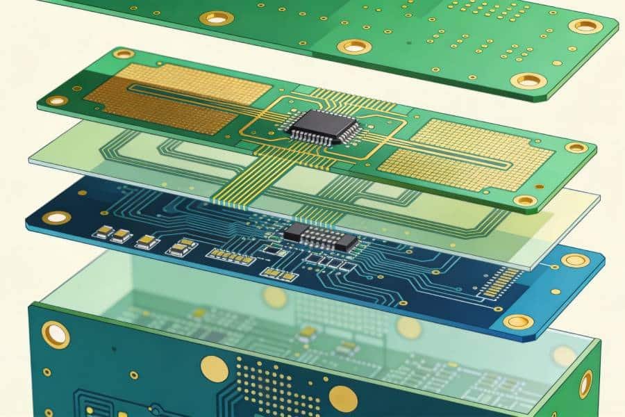
Mistake #1: Treating the Stackup as an Afterthought
What goes wrong
One of the most damaging high‑frequency mistakes is picking a generic multilayer stackup (or just accepting the CAD tool default) without coordinating with your PCB fabricator. Designers then calculate 50 Ω traces using assumed dielectric thickness and Dk values that do not match what the fab will actually build. The result is off‑target impedance, higher‑than‑expected loss, extra crosstalk between layers, and RF behaviour on the bench that does not match simulations. In more severe cases, poor copper balance or asymmetric layer arrangements even cause board warpage, which further changes spacing and impedance.
Why it hurts high‑frequency designs
At RF and multi‑GHz speeds, impedance and field distribution are set by the exact geometry and materials of your stackup: trace width, copper thickness, dielectric thickness, and dielectric constant. If the real dielectric layer under an RF microstrip is, say, 25–30% thicker than you assumed, your “50 Ω” line might come back at 60 Ω, causing reflections and return‑loss problems across the band. Putting high‑frequency layers too close to each other without an intervening plane makes crosstalk and EMI much worse, while a lack of symmetry in copper and dielectrics can create bow and twist that shift those spacings again in unpredictable ways.
How to do it correctly
The fix is to treat the stackup as a first‑class design object, not a post‑layout detail. Work with your PCB manufacturer at the start of the project to define a realistic stackup: actual FR4/Rogers/PTFE materials, dielectric thicknesses, copper weights, and which layers can serve as solid reference planes. Place your high‑frequency signal layers directly adjacent to continuous ground planes, keep the stackup as symmetrical as practical, and choose low‑loss dielectrics where long RF runs or very high frequencies demand it. Then feed this confirmed stackup into your impedance calculators and EM tools so that all “50 Ω” or “100 Ω” traces, and your simulation models, are based on the same physical reality the fab will deliver.
If you do not want to negotiate complex FR4/Rogers/PTFE stackups alone, you can involve our high‑frequency PCB manufacturing team early in your design to lock a buildable stackup before layout.
Mistake #2: Poor RF Component Placement and Partitioning
What goes wrong
A very common high‑frequency mistake is treating RF component placement like generic digital layout: parts are scattered wherever they fit, with no regard for the RF signal chain, isolation, or parasitics. Amplifiers, filters, and matching networks end up far apart, sensitive LNAs sit next to noisy regulators, and long “component‑to‑component” traces quietly add inductance and capacitance. In dense designs, RF, digital, and power circuits are often packed together without clear physical or electrical partitioning, which makes interference between blocks almost inevitable.
Why it hurts high‑frequency designs
At RF, every extra millimeter between components adds series inductance, shunt capacitance, and more coupling area to other signals. Long or meandering paths between a device and its matching network can detune the match, increase loss, and create unplanned feedback paths that lead to oscillations or spurs. Placing LNAs, VCOs, or mixers too close to digital clocks, switching regulators, or high‑power RF stages injects noise exactly where the circuit is most sensitive, degrading noise figure and dynamic range. Poor orientation of inductors, transformers, and resonant structures further increases magnetic coupling and distorts filter or balun responses.
How to do it correctly
Start placement by following the RF signal flow, not the mechanical outline: lay out the chain in order—antenna/connector → filters/duplexers → LNAs/PAs → mixers/IF—using short, direct paths. Keep each matching network compact and as close as possible to the device or port it serves, so that the interconnect does not become part of the network. Physically partition RF, digital, and power sections, with enough spacing and, where necessary, shields or grounded copper “moats” between noisy and sensitive areas. Within the RF zone, separate high‑power and low‑level stages, orient inductors and transformers to minimize coupling (often at right angles), and place oscillators close to their clock pins over a clean ground region. If you treat component placement as the first RF design decision on the PCB, routing, grounding, and EMC become much easier—and many “mystery” RF problems simply never appear.
Mistake #3: Ignoring Transmission‑Line Behaviour in Routing
What goes wrong
Another classic high‑frequency mistake is routing RF traces as if they were low‑speed wires: arbitrary widths, no controlled‑impedance rules, sharp 90° corners, long parallel runs, and frequent, casual layer changes. Designers sometimes mix trace geometries (microstrip, stripline, coplanar) on the same net without recalculating impedance or checking how each transition behaves. It is also common to see sensitive RF lines squeezed between other signals or power traces to “save space,” creating long sections of tightly coupled, parallel routing.
Why it hurts high‑frequency designs
At RF and multi‑GHz speeds, every critical trace is a transmission line whose impedance, delay, and coupling are set by its geometry and surroundings. If trace width and dielectric stackup do not match the intended 50 Ω (or other) impedance, you get reflections and return‑loss issues that show up directly in S‑parameter and eye‑diagram measurements. Sharp 90° bends locally change the effective width and impedance, and although the effect depends on frequency, they do add parasitic capacitance and can become small radiators in very high‑frequency applications. Long, closely spaced parallel runs between RF lines—or between RF and noisy digital—create strong capacitive and inductive coupling, which leads to crosstalk, AM/PM distortion, and intermittent failures that are hard to debug.
How to do it correctly
Define controlled‑impedance routing rules for all critical RF nets based on your confirmed stackup, and stick to a single, well‑understood geometry (microstrip, stripline, or coplanar waveguide) per segment. Keep RF traces short, direct, and on a layer with a solid, continuous reference plane directly underneath; when you need to change layers, minimize the number of transitions and design the via structure as part of the transmission line. Use 45° bends or smooth arcs instead of single 90° corners, especially in very high‑frequency paths, and avoid long, tightly spaced parallel runs between sensitive lines—add spacing, ground guard traces, or via fences to control coupling if proximity is unavoidable. With these habits, your routed RF paths will behave much closer to the ideal lines you used in simulation, and many “mystery” signal‑integrity problems disappear before the first prototype is built.
Mistake #4: Bad Grounding and Broken Return Paths
What goes wrong
Many high‑frequency boards still follow old “split the ground plane” advice: designers carve the ground into separate analog, digital, RF, and power islands, then inevitably route high‑speed or RF traces across the gaps. Others punch large slots and cutouts into the ground plane for mechanical features or thermal pads without adding via fences or alternate return paths. It is also common to see very sparse stitching vias between ground regions and layers, leaving pieces of “floating” copper that are not well tied into the main reference plane.
Why it hurts high‑frequency designs
At RF, the ground plane is part of the transmission line, not just a big copper pour for “safety.” When a signal trace crosses a split or large gap in its reference plane, the return current is forced to detour around the opening, greatly increasing loop area and inductance, which in turn raises EMI and degrades signal integrity. Multiple disconnected grounds—analog, digital, RF—often create exactly the opposite of what was intended: noisy shared return paths, common‑impedance coupling, and radiated emissions that show up as EMC test failures. Large ground cutouts and poorly tied “islands” behave like antennas or resonant structures, further worsening high‑frequency behaviour.
How to do it correctly
For most modern mixed‑signal and RF boards, the safest default is a single, continuous ground plane with careful functional partitioning in placement and routing, rather than physically split planes. Put RF and high‑speed signal layers directly adjacent to solid, unbroken ground and avoid routing any critical trace over a plane split, slot, or large cutout. Use plenty of stitching vias to tie ground regions and layers together—especially along board edges, around RF zones, and beside any signal via transitions—so return currents always have a short, low‑impedance path. When you truly must create local clearances (for example under thermal pads or chassis features), keep them small and surround them with a ring of ground vias to preserve shielding and reference continuity as much as possible.
Mistake #5: Via Stubs and Poor RF Via Transitions
What goes wrong
On many high‑frequency boards, through‑hole vias are dropped onto RF nets without considering the unused barrel length or how the transition behaves as part of the transmission line. Signals might only need to travel between two adjacent inner layers, but the via is drilled all the way through the stack, leaving a long via stub above or below the active connection. Designers also often omit nearby ground return vias, use oversized antipads, or cluster many vias tightly together, all of which disturb the local impedance and increase coupling between channels.
Why it hurts high‑frequency designs
Every via on a high‑speed or RF path behaves as an inductive and capacitive discontinuity, and the unused portion—the stub—acts like a small, unterminated transmission line. As frequency rises, via stubs create impedance discontinuities that cause reflections and can resonate at quarter‑wavelength and odd harmonics, carving deep notches in the channel’s frequency response and degrading S‑parameters. This shows up as extra insertion loss, phase distortion, and sometimes complete collapse of signal amplitude around the stub’s resonance, especially in multi‑GHz and mmWave designs. Lack of nearby ground vias and poorly shaped antipads further increase return‑loss and crosstalk by forcing return currents to spread out and interact with neighboring structures.
How to do it correctly
First, minimize via transitions on critical RF paths; keep sensitive lines on one layer where possible, or limit them to a single, well‑designed transition. When you must change layers, reduce or eliminate via stubs by using blind/buried vias in HDI stackups, or specify backdrilling to remove the unused barrel portion on thick or high‑frequency boards. Design each RF via as part of the transmission line: choose appropriate drill size, pad, and antipad, place one or more ground return vias close to the signal via, and avoid unnecessary via clusters that crowd the field and create extra coupling. For very high‑performance channels, model the via transitions in a 3D EM tool and verify that their contribution to return‑loss and insertion‑loss is acceptable across your operating band.
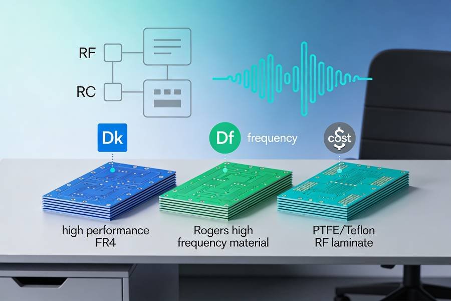
Mistake #6: Using the Wrong PCB Materials for High Frequency
What goes wrong
A frequent high‑frequency mistake is defaulting to standard FR4 for everything—even multi‑GHz RF paths and long high‑speed links—simply because it is cheap and familiar. Sometimes designers do the opposite: they specify exotic RF laminates everywhere, even for low‑speed logic and power, driving cost up with little real benefit. In other cases, teams mix materials (FR4 plus high‑frequency laminates) without understanding differences in dielectric constant, loss, or CTE, which leads to inconsistent impedance and reliability issues.
Why it hurts high‑frequency designs
FR4 has relatively high and variable dielectric constant and loss tangent, so at high frequencies it causes much more attenuation and makes precise impedance control difficult. As frequency and trace length increase, this extra loss can easily exceed the link budget, while Dk variation with frequency, temperature, and moisture shifts impedance and phase in ways your simulations did not include. In contrast, high‑frequency materials like Rogers and PTFE offer lower loss and more stable Dk, but if they are used without considering CTE and process compatibility, you can encounter warpage, delamination, or yield problems in multilayer builds.
How to do it correctly
Match the material to the job: use FR4 for low‑frequency, short, or less critical sections; step up to Rogers‑class laminates when you need lower loss and stable Dk into the multi‑GHz range; and reserve PTFE‑based materials for very high‑frequency or ultra‑low‑loss RF paths. For many designs, a hybrid stackup—high‑frequency laminate only on RF and antenna layers, FR4 elsewhere—delivers the required performance without overspending on the entire board. Always base your simulations and impedance calculations on the actual material data (Dk/Df vs. frequency and temperature) from the laminate vendor, and coordinate early with your PCB manufacturer to confirm availability, CTE compatibility, and process limits for your chosen materials.
Mistake #7: No DFM/DFT Thinking Before Releasing RF Boards
What goes wrong
A final, very common mistake is treating high‑frequency PCB design as “done” once the layout looks clean on screen, without checking whether it can be built and tested reliably. Designers skip a focused DFM/DFT review for RF: no clear impedance‑control notes, no test coupons, no thought about connector placement or calibration structures, and minimal test access on power and control nets. Manufacturing limits like minimum trace/space, drill sizes, annular ring, solder‑mask clearances, and assembly constraints are often assumed rather than confirmed with the fab and assembler.
Why it hurts high‑frequency designs
A design that works in EM/schematic simulation but ignores DFM can fail in production with impedance variations, unexpected losses, and low yield. Without test coupons, the fabricator has no easy way to verify controlled impedance, and you have no simple reference when S‑parameters look wrong on the bench. Lack of RF‑friendly connectors, launch structures, or test points makes it hard to measure and debug the actual board, so small issues in stackup, vias, or grounding turn into time‑consuming lab work and extra spins. Ignoring DFM/DFT also drives up assembly problems—tombstoning, poor solder joints, rework—which can mask or be confused with RF issues.
How to do it correctly
Bake RF‑focused DFM and DFT into your design flow before you release Gerbers. Agree with your fabricator on controlled‑impedance requirements, add appropriate impedance test coupons for each critical line type, and document stackup, materials, and impedance targets clearly in the fab notes. Provide practical RF access: coax connectors or well‑defined launches at key ports, plus test pads or vias on important supplies, control lines, and representative transmission lines so you can probe and tune without cutting traces. Run at least one joint DFM review with your PCB and assembly vendors to check trace/space, drills, via fills, solder‑mask openings, and component footprints against their real process limits. With this in place, your high‑frequency boards are far more likely to work electrically, pass compliance, and move smoothly from prototype into volume production.
Our RF PCB DFM and prototyping services can review your Gerber, stackup, and impedance notes before release to catch many of these issues early.
Mistake #8: Overlooking Assembly Details That Matter More at High Frequency
What goes wrong
Many high‑frequency designs reach the fab with beautiful RF layout but weak assembly details: incorrect or non‑IPC‑compliant footprints, oversized copper pours under RF parts, no solder‑mask dams between fine‑pitch pads, or generic stencil settings that under‑ or over‑print solder paste. Designers also tend to ignore how solder mask and its thickness affect impedance on microstrip and coplanar lines, especially when mask openings or different mask types are used along the same RF path.
Why it hurts high‑frequency designs
Footprint and assembly problems show up as tombstoned capacitors, skewed inductors, voided ground pads, and inconsistent contact resistance—all of which directly change the effective values and loss of RF components and transmission lines. Misaligned or floating parts in matching networks and filters can detune the response, while poor thermal reliefs and reflow profiles on RF laminates lead to delamination or subtle changes in dielectric properties over time. On top of that, solder mask with high Dk/Df or uneven thickness along RF traces alters impedance and loss, especially above a few gigahertz, so an assembly‑driven change in mask or thickness can quietly shift your carefully tuned lines.
How to do it correctly
Treat footprints, solder mask, and stencil design as part of the RF design, not just an assembly afterthought. Use up‑to‑date manufacturer libraries or carefully checked IPC‑based footprints, follow datasheet recommendations for exposed pads and thermal reliefs, and coordinate stencil apertures with your assembler to get consistent, void‑free joints on RF components. Keep solder mask behaviour in mind: avoid random mask openings or type changes along RF traces, and if your frequency or loss budget is tight, discuss low‑loss, lower‑Dk mask options and thickness control with your PCB vendor. By closing this “last mile” between layout and assembly, you reduce the risk that mechanical or process details will quietly undo the RF performance you designed for.
Conclusion: Turn “Gotchas” into a Pre‑Release Checklist
High‑frequency PCBs rarely fail because of one dramatic error; they usually fail because several small mistakes stack up—an approximate stackup, sloppy placement, casual routing, weak grounding, problematic vias, the wrong materials, and missing DFM/DFT details. The good news is that all eight mistakes in this article are predictable and repeatable, which means they can be caught systematically before you ever send Gerbers out.
If you turn these points into a simple pre‑release checklist—“Did we lock stackup with the fab? Is RF placement clean? Are all critical lines controlled‑impedance? Are ground planes continuous? Are via stubs under control? Are materials appropriate? Did we review RF DFM/DFT and assembly details?”—you dramatically improve the odds of first‑pass success. Over time, that checklist becomes part of your standard design review process, reducing risk, saving spins, and letting your team focus on pushing RF performance rather than firefighting avoidable layout mistakes.
When you are ready to turn your improved high‑frequency design into hardware, you can send us your files and requirements—our high‑frequency RF PCB fabrication and assembly services cover everything from quick‑turn prototypes to volume production on FR4, Rogers, and PTFE.