Table of Contents
Why High Frequency PCB Cost Is Different
High frequency PCB cost behaves very differently from standard FR‑4 board pricing, because you are paying not only for copper and area but also for RF‑grade materials, tighter process control, and specialized testing. As soon as you move into RF and microwave frequencies, factors such as dielectric loss, impedance stability, insertion loss, and phase consistency start to dominate performance; meeting these requirements often means using premium laminates like Rogers or PTFE, more complex stackups, and narrower manufacturing tolerances—all of which drive up RF PCB manufacturing cost. On top of that, small prototype batches, hybrid material builds, and advanced options such as blind/buried vias, backdrilling, or detailed RF test reports can quickly multiply the price per board if they are not planned carefully.
For RF designers and hardware teams, the challenge is to balance performance and budget instead of accepting every cost increase as “the price of going high frequency”. In the following sections, we will break down the key RF PCB manufacturing cost factors—materials, stackup and size, design complexity, process and test, volume and lead time—and then show practical optimization tips you can use to control high frequency PCB cost without compromising the electrical performance your application actually needs.
In the following sections, we will break down the key RF PCB manufacturing cost factors… and show how to optimize them through smarter material choices, design decisions, and closer collaboration with your high frequency PCB manufacturer.
Cost Driver 1 – High Frequency Materials (Rogers, PTFE, Low‑Loss FR‑4)
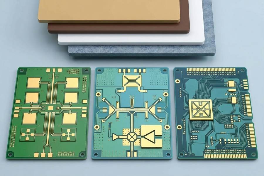
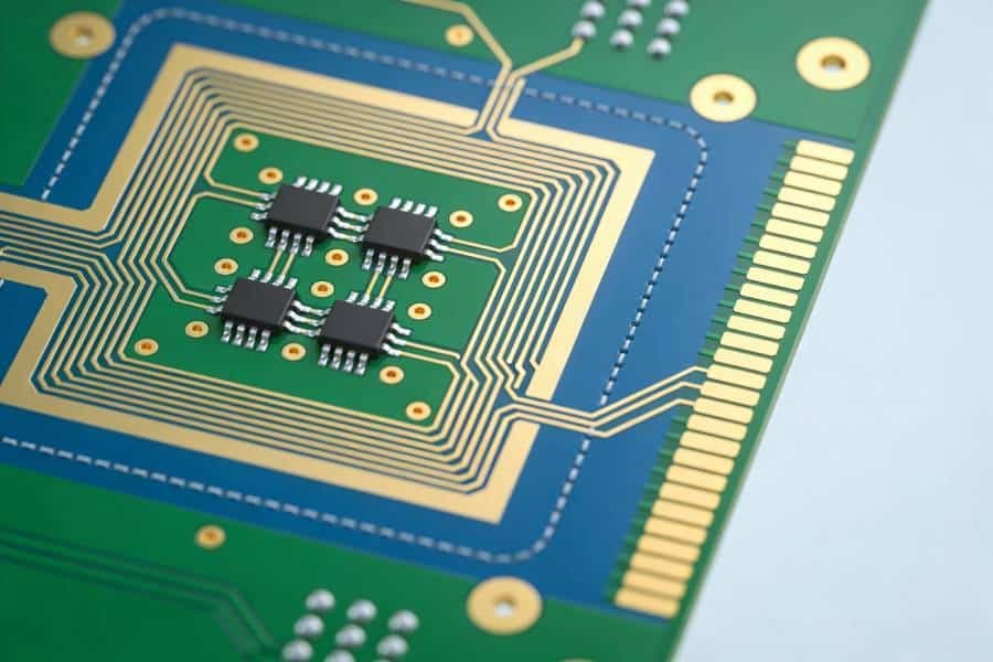
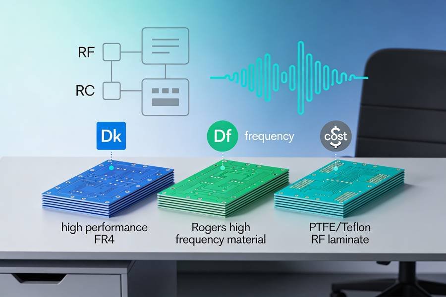
The single biggest driver of high frequency PCB cost is usually the substrate material you choose. Standard FR‑4 is extremely economical, typically only a fraction of the price of engineered RF laminates, but its higher and less stable dielectric constant and loss tangent make it unsuitable for many serious RF and microwave designs. By contrast, Rogers‑class hydrocarbon and ceramic laminates, as well as PTFE‑based materials, offer much lower Dk/Df and far better stability over frequency and temperature, which is why they are widely used in 5G, radar, and high‑speed digital systems—yet they can cost several times more per unit area than FR‑4 and often require additional processing steps.
Even within the “high frequency materials” family, costs vary significantly depending on the specific series, thickness, and copper weight. Mid‑range options such as RO4000‑class hydrocarbon laminates are generally more manufacturing‑friendly and closer to FR‑4 in processing, so their overall high frequency PCB cost impact is moderate, while ultra‑low‑loss PTFE or ceramic‑filled materials used for mmWave can easily push raw‑material costs to the top of your RF PCB manufacturing budget. Availability also matters: non‑standard thicknesses, unusual copper weights, or rarely used laminate families may require special ordering, longer lead times, higher minimum order quantities, and extra scrap, all of which show up in the final price per board.
From an optimization standpoint, you rarely want to “always pick the most expensive RF material”; instead, you want to match the laminate to your real performance needs while minimizing waste. A common strategy is to use a hybrid stackup, placing Rogers or PTFE only on the RF‑critical layers (for antennas, matching networks, filters, or ultra‑high‑speed channels) and using low‑loss FR‑4 or standard FR‑4 for non‑critical digital, control, and power layers; this can dramatically reduce high frequency PCB cost while preserving key RF performance. You can further optimize cost by favoring RF materials that your manufacturer keeps in regular stock (for example common RO4350B thicknesses), selecting standard laminate thicknesses and copper weights where possible, and avoiding unnecessary grade changes between prototypes and volume so that you do not pay multiple times for qualification and leftover material.
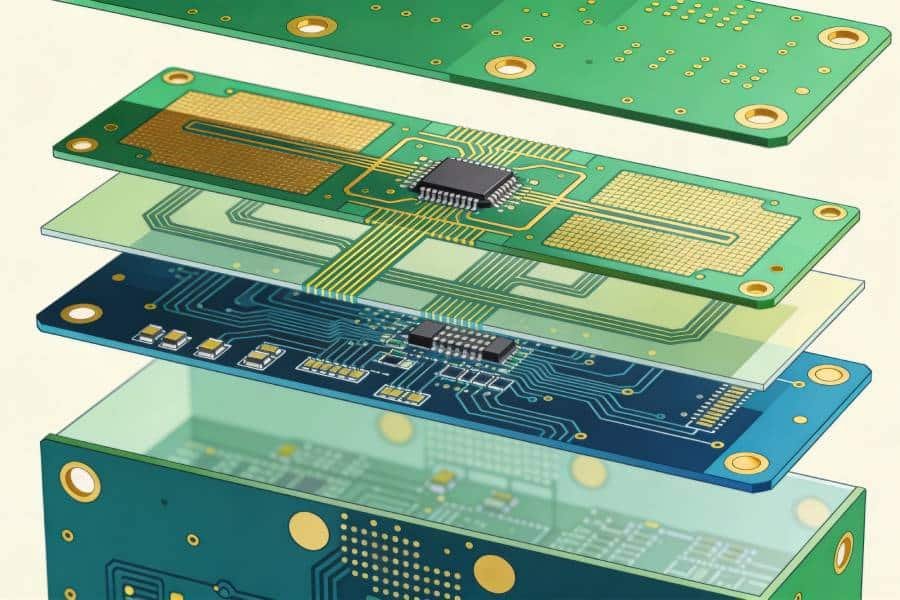
Cost Driver 2 – Stackup, Layer Count, and Board Size
Beyond materials, the way you build the stackup—and how big and complex the board is—has a major impact on high frequency PCB cost. Every extra layer adds dielectric, copper, lamination cycles, registration steps, and potential yield loss, so moving from a 4‑layer to 6‑layer, or 6‑layer to 8‑layer RF stackup can easily increase board cost by 20–40% per added layer pair, especially in small and medium volumes. Thicker boards and special copper weights (for example 2 oz or heavier planes) compound this effect, because they require more material and can force slower drilling and plating recipes in manufacturing.
Board outline and panel utilization then determine how efficiently those layers are used. Large or awkwardly shaped RF PCBs may only fit a few units on a standard production panel (commonly around 18 × 24 inches), which means you are paying for a lot of unused laminate and copper, while a well‑chosen outline that tiles cleanly can significantly reduce the per‑unit high frequency PCB cost. In practice, poor panelization can raise unit cost by 15–25% for multilayer designs, whereas even a 10% improvement in panel utilization can translate into meaningful savings over the life of a project.
To optimize RF PCB manufacturing cost in this area, treat stackup and size as design parameters you can negotiate, not as fixed constraints. Start by questioning whether you truly need each additional layer: with careful placement, return‑path control, and via planning, many designs can step down from 8 layers to 6, or 6 to 4, without sacrificing RF performance, often cutting total board cost by 20–35%. At the same time, involve your PCB manufacturer early to co‑design panelization and target standard panel sizes; small adjustments to board dimensions, break‑off tabs, or the decision to split a very large RF assembly into two smaller modules can dramatically improve panel yield and keep high frequency PCB cost under control.
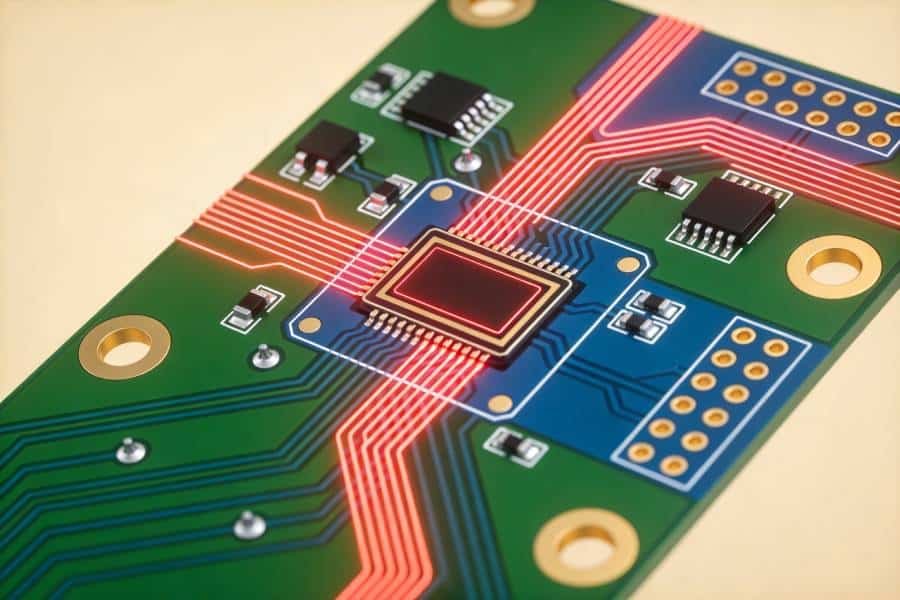
Cost Driver 3 – RF Design Complexity and Tolerances
RF design complexity is another major, and often underestimated, contributor to high frequency PCB cost. Very fine trace widths and spacings, dense coupling structures, intricate antenna arrays, and aggressive via schemes (blind, buried, microvias) all require more advanced imaging, drilling, and plating processes, which increase setup time, scrap risk, and therefore the price per board. For example, moving from “standard” 4–6 mil design rules to sub‑4 mil lines and spaces can add 15–20% to PCB fabrication cost because it forces the use of high‑end LDI exposure and tighter etch control, while each blind or buried via can cost several times more than a simple through‑hole due to extra drilling and lamination steps.
Tight electrical tolerances compound this effect in high frequency designs. Specifying very narrow impedance or phase‑matching windows (for example ±5% impedance or sub‑degree phase matching over long RF paths) drives the factory to use stricter control of trace width, dielectric thickness, registration, and copper thickness, which typically reduces yield and pushes up RF PCB manufacturing cost. As a rough guideline, moving from ±10% to ±5% impedance tolerance can add 30% or more to the cost of the controlled‑impedance portion of a design, while pushing down to ±3% can increase cost by 50% or higher because many boards fall out of spec and must be scrapped or reworked. Similar trade‑offs apply to length‑matching and skew constraints in phased arrays or multi‑channel RF front‑ends, where very tight matching often demands additional meanders, vias, and tuning features that further complicate fabrication.
From a cost‑optimization perspective, it is important to reserve this level of complexity and tight tolerance only for the parts of the design that truly need it. Many RF boards can relax trace geometries and tolerances on non‑critical control, power, and low‑frequency sections, while keeping strict rules only on high‑Q filters, antennas, couplers, and high‑speed links; this allows the manufacturer to treat only a subset of the board as “premium RF” and fabricate the rest with more forgiving, lower‑cost rules. Likewise, thoughtful via planning—using blind or microvias only where they actually reduce layer count or enable critical routing density—can turn an apparent cost adder into a net saver by allowing you to drop one or two layers from the stackup. The key is to discuss these trade‑offs early with your PCB supplier so that RF performance and manufacturability are balanced intentionally instead of discovering late that an overly complex layout has made your high frequency PCB cost explode.
Cost Driver 4 – Manufacturing Process, Yield, and Testing
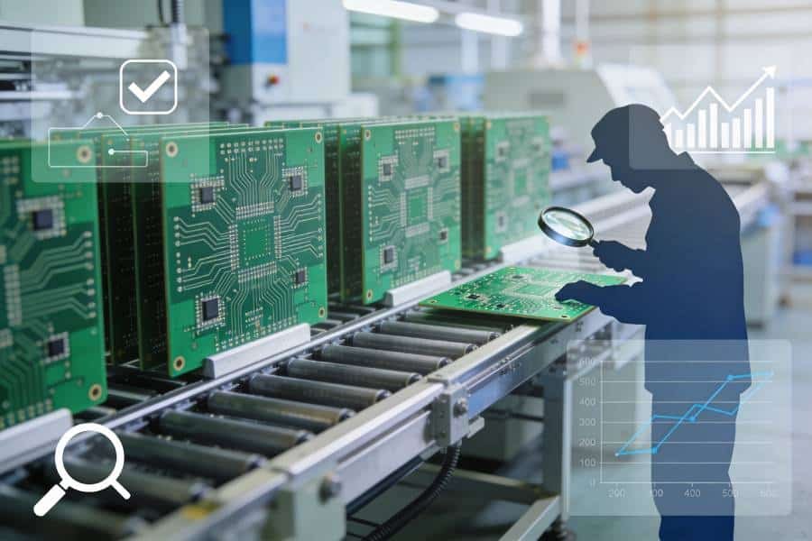
High frequency PCBs often require more advanced processes than standard boards, and each extra step adds both direct cost and yield risk. RF laminates like Rogers and PTFE can need plasma or special chemical treatments for hole wall preparation, tighter etching control for fine RF features, precise backdrilling, and more careful lamination, which together make high frequency / RF PCB etching and processing 30–60% more expensive than conventional FR‑4 in many cases. When the process window is narrow, early builds tend to have lower yield, so manufacturers factor expected scrap and rework into the quoted price; in practice, this “yield premium” can easily add double‑digit percentages to high frequency PCB cost until the process is stabilized.
Testing is another non‑trivial part of RF PCB manufacturing cost, especially when you need more than a simple electrical continuity check. For controlled‑impedance and high‑speed RF structures, board shops may run TDR measurements on coupons or even insertion‑loss tests using Delta‑L or full VNA‑based methods, which require specialized equipment, extra coupons, and operator time, all charged into the cost of the lot. Structural tests like flying‑probe or fixture‑based in‑circuit testing add further cost: flying probe is more economical for small batches but carries a higher per‑board test fee, while fixtures have high upfront cost that only pays off in volume. To keep RF PCB manufacturing cost under control, it is important to define a test strategy that targets the real risks—such as impedance, opens/shorts, and critical RF paths—without over‑specifying 100% high‑end RF measurements where a well‑designed sampling plan or coupon‑based approach would provide sufficient confidence.
Cost Driver 5 – Volume, Panelization, and Lead Time
High frequency PCB cost is very sensitive to order volume because setup, tooling, programming, and engineering time are largely fixed per build and must be amortized over the number of boards. Prototype and small‑batch RF runs therefore carry a much higher cost per unit—often several times the eventual mass‑production price—while scaling volume by a factor of 10 can reduce unit cost by roughly 30–40% once those fixed costs are spread across more boards. This effect is even stronger for high frequency PCBs that use expensive Rogers or PTFE laminates, because scrap, coupons, and leftover panel edges represent a larger share of the total material budget when quantities are low.
Panelization ties directly into how efficiently that material is used and how many boards can be processed per manufacturing cycle. Well‑designed panels that fit many RF boards per production panel reduce waste and handling time, often lowering total PCB and assembly cost by 20–30% on larger runs, whereas irregular shapes or oversized single boards can leave large unused areas and require more machine setups. Lead time is the final lever: expedited fabrication compresses standard 1–3 week cycles into a few days, but express surcharges for high frequency PCBs can add 20–50% or more to the base price because the factory must reserve capacity, prioritize special materials, and sometimes run off‑shift to meet the deadline. Whenever schedule allows, grouping RF orders into slightly larger batches, coordinating panelization with your manufacturer, and avoiding unnecessary rush orders are some of the simplest ways to keep high frequency PCB cost under control without changing the underlying design.
Practical Strategies to Optimize High Frequency PCB Cost
After you understand the main RF PCB manufacturing cost factors, the next step is to consciously design and source for cost, not just for performance. In practice, most savings come from a handful of structural decisions: choosing the right material mix, avoiding unnecessary stackup and layout complexity, designing within standard manufacturing limits, and aligning your ordering pattern with how PCB factories actually run their lines.
On the material side, match the laminate to the real electrical and thermal requirements instead of reflexively specifying the most expensive RF option. For example, many designs under about 1–2 GHz can use high‑Tg or low‑loss FR‑4, and many 3–6 GHz applications can tolerate mid‑range low‑loss materials instead of full PTFE, especially if you optimize trace geometry and stackup. Hybrid stackups, where only the RF‑critical layers use Rogers or PTFE and the rest use FR‑4, often deliver 15–25% material savings while meeting high frequency performance targets.
On the design side, embrace Design for Manufacturability (DFM) as early as possible. Stay within your manufacturer’s standard design rules for trace width/spacing, drill sizes, aspect ratios, and copper weights whenever you can, and reserve ultra‑fine features or exotic via structures only for areas where they are truly needed. Systematically reviewing RF layouts with your PCB supplier can reveal opportunities to drop one or two layers, simplify via schemes, loosen non‑critical tolerances, and improve panelization—each of which can shave 10–30% off high frequency PCB cost without hurting SI or RF behavior when done carefully.
Finally, optimize how you order and collaborate. Whenever schedule allows, consolidate small prototype quantities into slightly larger batches, or combine multiple RF variants on the same panel, so fixed engineering and setup costs are spread over more boards. Share target price ranges and flexibility with your RF PCB manufacturer up front, then ask them to propose one “performance‑maximized” and one “cost‑optimized” build variant; comparing these options will highlight which material, stackup, or tolerance changes offer the largest savings per dB of loss or per percentage point of impedance tolerance.
How to Work with Your RF PCB Manufacturer on Cost
High frequency PCB cost is much easier to control when you treat your RF PCB manufacturer as a design partner rather than just a price‑taker at the end of the process. The most effective collaborations start early: sharing preliminary stackups, target frequencies, loss budgets, and approximate cost targets at the concept stage gives your supplier room to suggest alternative materials, layer counts, and via strategies that fit both performance and budget. Many specialized RF PCB shops now offer formal cost‑optimization or DFM reviews where they walk your layout against their specific process limits and highlight “cost hot spots” such as overly fine geometries, unnecessary blind vias, or non‑standard board thicknesses.
Clear communication about trade‑offs is essential. Instead of simply demanding “lowest high frequency PCB cost,” provide a prioritized list: which RF paths absolutely need the lowest insertion loss, which impedance or phase‑matching tolerances are critical, and where you can accept slightly more loss or looser tolerances in exchange for cost savings. Ask your manufacturer to quote at least two variants—a performance‑first build and a cost‑optimized build—so you can see exactly how changes in material grade, stackup, via technology, or test coverage affect RF PCB manufacturing cost. Over time, building a regular feedback loop around yield reports, test results, and NPI lessons learned allows both sides to refine design rules and preferred stackups, turning one‑off optimizations into a repeatable, lower‑cost way of doing high frequency business together.
Summary Checklist for Controlling High Frequency PCB Cost
You can use this quick checklist at each design spin or RFQ to keep high frequency PCB cost under control.
- Material choice: Have you matched the laminate to your real frequency and loss needs, and considered hybrid stackups (Rogers/PTFE only on RF‑critical layers, FR‑4 elsewhere)?
- Stackup and layers: Can you safely reduce layer count, avoid exotic thicknesses, and stay close to your manufacturer’s standard stackups and copper weights?
- Board size and panelization: Does your outline tile efficiently on common panel sizes, and have you asked your fabricator for a recommended panelization to minimize waste?
- RF design complexity: Are ultra‑fine geometries, dense arrays, and blind/buried or microvias limited to places where they genuinely improve RF performance or enable layer reduction?
- Tolerances: Have you reserved the tightest impedance and phase‑matching specs only for truly critical nets, while relaxing tolerances on non‑critical regions to boost yield?
- Process steps: Do you understand which special processes (plasma treatment, backdrill, advanced etch, etc.) are being used, and have you confirmed they are all necessary for your goals?
- Test strategy: Is your plan for TDR, insertion‑loss, and electrical tests focused on real risk, using sampling or coupon‑based measurements where appropriate to avoid over‑testing every board?
- Volume and lead time: Can you consolidate prototypes, slightly increase batch size, or relax lead time to reduce setup and expedite surcharges on high frequency PCB orders?
- DFM collaboration: Have you run at least one joint DFM/cost‑review with your RF PCB manufacturer before freezing the design, and requested a “cost‑optimized” alternative build for comparison?
- Long‑term alignment: Are you reusing proven, cost‑effective RF stackups and design rules across projects to avoid re‑qualifying materials and processes every time?