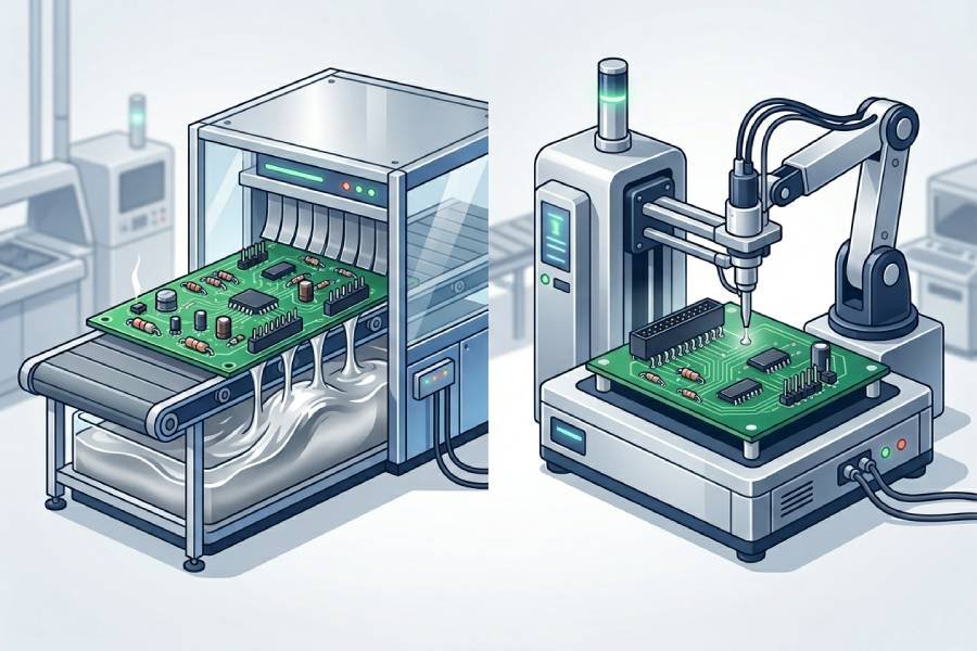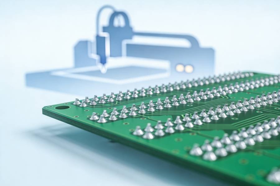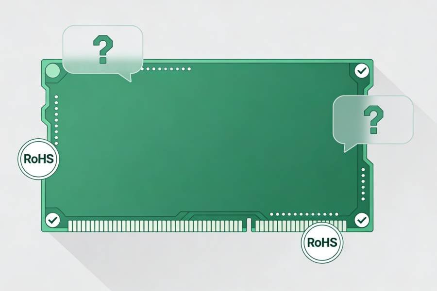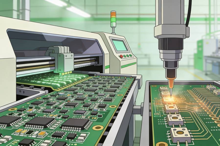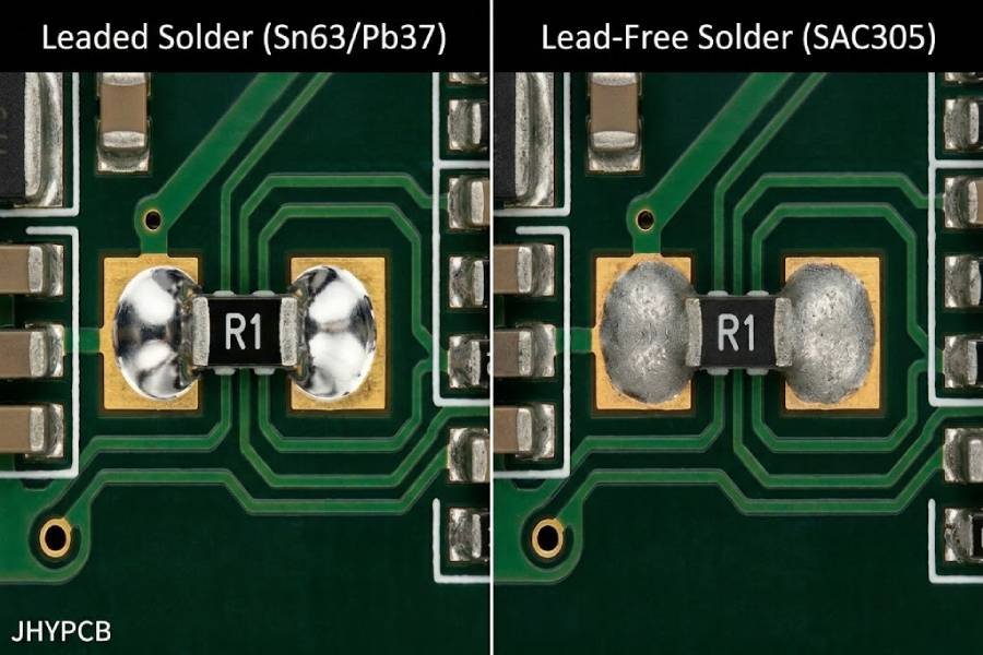
Lead-Free vs. Leaded Solder in SMT Assembly: A Comprehensive Guide to Compliance and Reliability
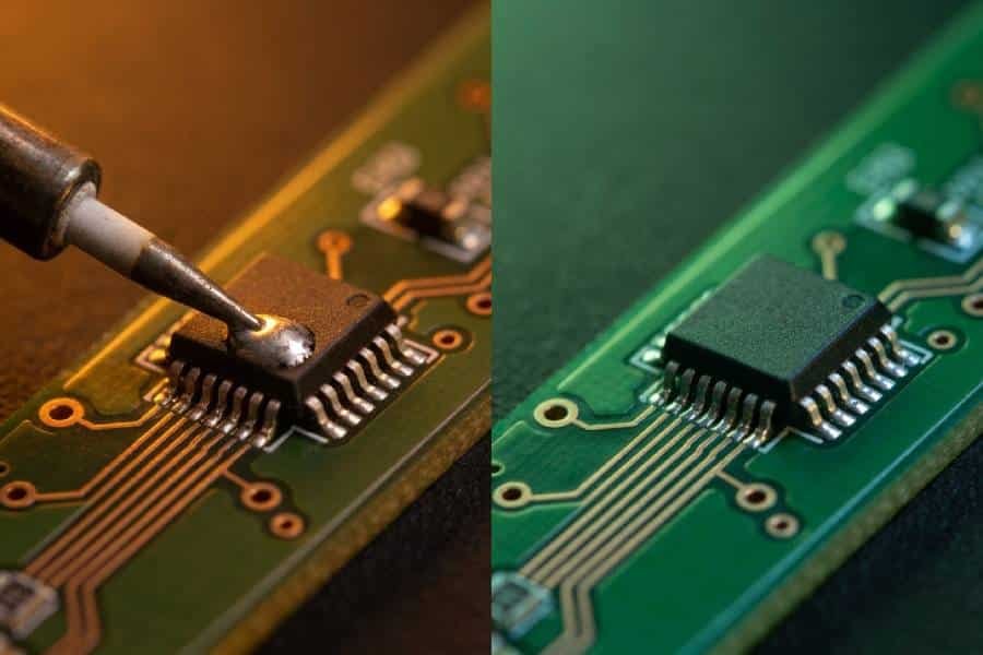
While Lead-Free solder is the global standard for RoHS compliance, Leaded solder remains critical for high-reliability sectors like aerospace. This guide compares their technical performance, manufacturing challenges, and how JHYPCB ensures zero-defect assembly for both processes.