Table of Contents
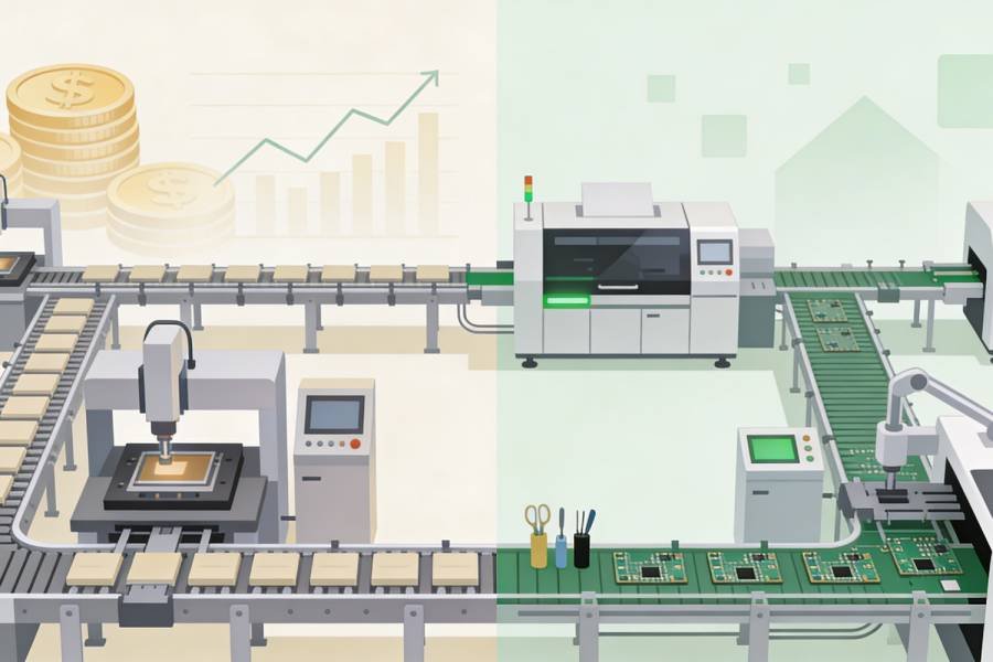
Lead-free through-hole assembly has to balance two competing goals: high throughput and tight control of solder quality around increasingly dense, mixed-technology designs. For many years, wave soldering has been the default choice for tin‑lead and lead-free through-hole boards, offering fast, cost-effective processing when the layout is “wave‑friendly.”
As component density and nearby SMT keep‑out requirements have tightened, selective soldering has emerged as a complementary process that delivers localized heating and highly controlled hole fill on exactly the joints you care about. This article compares wave soldering and selective soldering in lead-free through-hole assembly, outlining how each works, their main strengths and limitations, and how to choose the right approach for your next PCB design.
Basics of Lead-Free Through-Hole Soldering
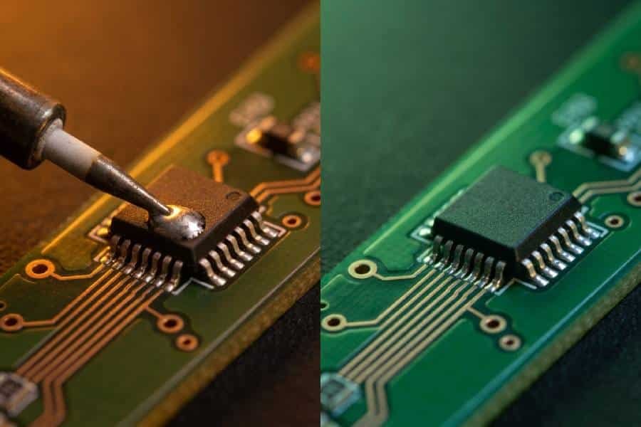
Lead-free through-hole soldering has the same basic goal as its tin‑lead predecessor: create a fully wetted, mechanically robust fillet that fills the plated‑through hole and bonds reliably to both the lead and the barrel. What changes with lead-free is the thermal budget and the wetting margin—you typically need higher temperatures, tighter process control, and more attention to flux chemistry to achieve the same hole‑fill and joint quality.
In wave and selective soldering, common lead-free alloys such as SAC305 melt around 217–221°C and usually require solder pot temperatures in the 250–270°C range, along with higher topside preheat, to drive solder up through the barrels and meet IPC hole‑fill criteria. Because lead-free alloys wet more slowly and with less inherent “forgiveness” than tin‑lead, board design (lead‑to‑hole ratio, annular ring, thermal reliefs) and surface condition (finish, cleanliness, moisture) have a much stronger influence on whether you see solid, shiny fillets or defects like cold joints, insufficient fill, and bridging.
At the same time, the higher pot and preheat temperatures put more stress on laminates and bottom‑side components, especially on thick, high‑layer‑count boards or assemblies that see multiple soldering cycles. That is why choosing between wave soldering and selective soldering in a lead-free environment is not just a question of throughput—it is also about how much localized thermal control you need, how complex the board is, and how tight your reliability requirements are.
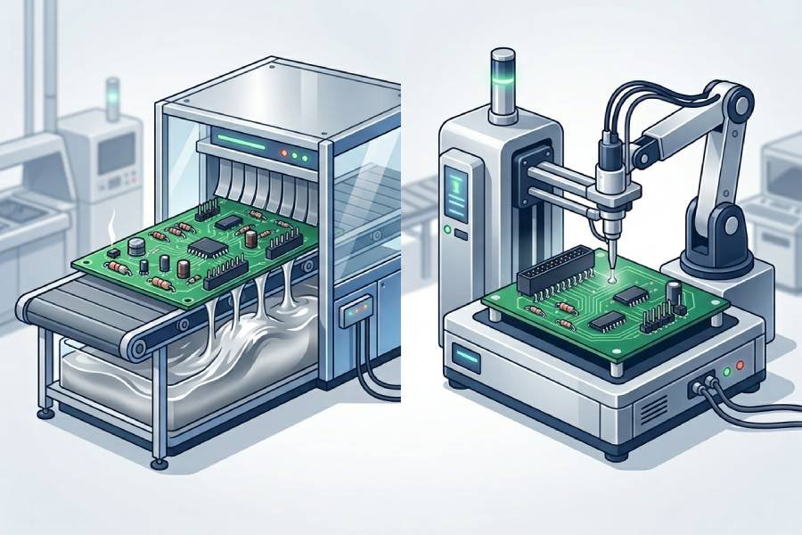
Wave Soldering in Lead-Free Through-Hole Assembly
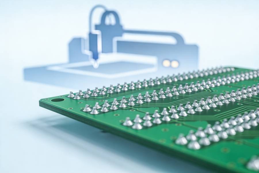
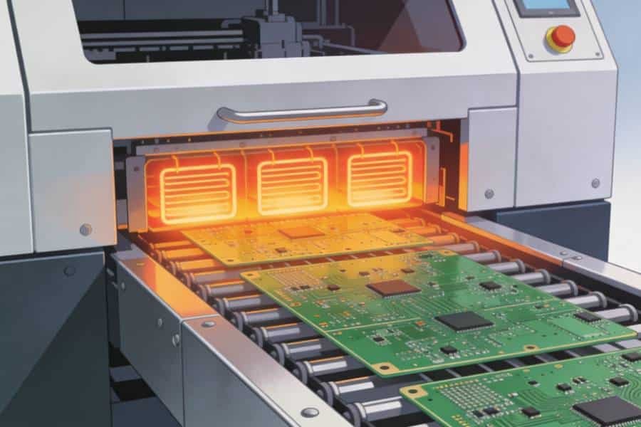
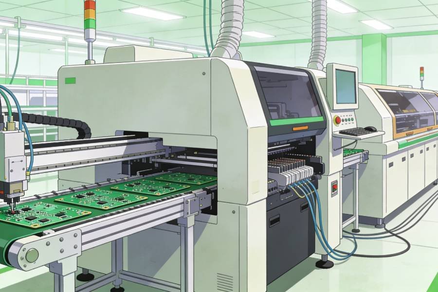
Wave soldering uses a standing “wave” of molten solder to simultaneously solder all exposed through-hole leads (and any bottom‑side SMT pads that are not masked) as the PCB passes over the solder pot on a conveyor. In a typical lead-free wave process, the board first passes through flux application and preheat zones to activate flux and gently raise the assembly temperature, then crosses one or more solder waves held around 255–270°C, and finally cools down so the solder fillets can solidify. With the right flux chemistry, preheat, conveyor speed, and contact time, the wave wets each lead, pulls solder up through the plated barrel, and forms continuous fillets that meet IPC hole‑fill requirements.
Lead-free wave soldering differs from tin‑lead primarily in its narrower process window. Higher pot temperatures, slower wetting, and greater surface tension mean flux selection, topside preheat, and contact time have a stronger impact on bridging, icicles, and incomplete hole fill. On dense, mixed‑technology boards, pallets or titanium masks are often needed to shield bottom‑side SMT parts from the wave, which adds complexity to setup and limits flexibility if the layout changes. Large or very thick boards may also need carefully optimized profiles and possibly nitrogen to ensure consistent topside temperatures and acceptable lead‑free hole fill across the entire panel.
When the layout is “wave‑friendly”—through-hole components grouped on one side, adequate keep‑out for bottom‑side SMT, good lead‑to‑hole ratios, and sensible thermal reliefs—wave soldering remains extremely attractive. It offers high throughput, strong and repeatable joints, and low cost per board in medium‑ to high‑volume lead-free production, making it a natural choice for traditional THT assemblies and for designs that can be consciously optimized around the wave process.
Selective Soldering in Lead-Free Through-Hole Assembly
Selective soldering applies molten solder only to specified through-hole joints using a programmable nozzle and motion system, instead of exposing the entire PCB to a full solder wave. In a typical lead-free selective process, the board is fluxed in the target areas, preheated (often from both top and bottom), and then a small solder fountain or nozzle—fed from a pot running around 260–280°C for SAC alloys—moves point‑to‑point under the programmed pins or connector rows. By controlling nozzle diameter, stand‑off height, dwell time, and drag speed for each joint, the process can deliver very consistent wetting and hole fill with minimal thermal exposure to the rest of the assembly.
Because only specific areas are heated and soldered, selective soldering is particularly well suited to dense, mixed‑technology boards where bottom‑side SMT sits close to through-hole pins and cannot tolerate a full wave. There is usually no need for pallets or mechanical masks, and nitrogen is commonly used at the nozzle to limit oxidation and dross formation, which is critical when working with small or fine nozzles and higher lead-free temperatures. The same flexibility also makes it easier to tune profiles for difficult joints—such as large connectors, heavy ground pins, or thick backplanes—by giving them longer dwell or a different nozzle path without affecting the rest of the board.
The trade‑off is throughput and complexity. Compared with a well‑optimized wave line, point‑to‑point selective soldering is inherently slower for boards dominated by through-hole content, because joints are soldered sequentially rather than all at once. Programming paths, optimizing flux and preheat for each product, and maintaining nozzle performance require more up‑front engineering effort and operator skill than a mature wave process. However, for high‑density mixed‑technology assemblies, frequent product changeovers, and applications where lead-free reliability and low defect rates are more important than absolute maximum throughput, selective soldering often provides the safer and more controllable process window.
Wave vs. Selective: Side-by-Side Comparison
At a high level, wave soldering favors speed and cost on wave‑friendly, through‑hole‑heavy designs, while selective soldering favors precision and flexibility on dense, mixed‑technology boards where nearby SMT and reliability are the main constraints.
Key differences at a glance
| Dimension | Wave soldering | Selective soldering |
|---|---|---|
| Process scope | Solders all exposed areas that see the wave; pallets or masks needed to protect bottom‑side SMT. | Solders only programmed joints with a nozzle; no pallets needed in most mixed‑tech layouts. |
| Throughput | Very high UPH on connector‑dense, pure‑THT boards; ideal for long, stable runs. | Slower because joints are soldered sequentially; scalable with multi‑nozzle systems but rarely matches wave on pure‑THT mass production. |
| Defect profile | More prone to bridging, icicles, and SMT shadowing issues on dense layouts if pallets/profile are not well tuned. | Much lower risk of bridging and SMT overheating; better control of hole fill on difficult connectors and thick boards. |
| Design constraints | Needs “wave‑friendly” grouping of THT, generous keep‑out around bottom‑side SMT, and careful lead‑to‑hole design. | Handles tight SMT adjacency and irregular connector placement better; more forgiving for complex and high‑density layouts. |
| Thermal impact | Entire bottom side sees flux, preheat, and wave; higher overall thermal stress on laminate and components. | Heat is localized to target joints; significantly lower thermal exposure for nearby SMT and board areas. |
| Setup & changeover | Faster to set up once pallets and parameters are dialed‑in; less flexible if products change frequently. | More programming effort per product, but easier to adapt to variants and frequent changeovers without new pallets. |
| Cost & TCO | Lower equipment cost and cost/board at high utilization on wave‑friendly products; pallets add cost for complex boards. | Higher CAPEX and setup cost, but less rework, no pallets, and better economics for complex, lower‑to‑mid volume or high‑reliability builds. |
How this plays out in practice
On a traditional, connector‑heavy power supply or backplane where most components are through‑hole and the layout can be grouped for the wave, a lead-free wave line usually delivers the lowest cost per board once fixtures and profiles are optimized. Defect modes like bridging or icicles can be kept under control with good design rules, pallets, and process tuning, and the throughput advantage is hard to beat in medium‑ to high‑volume production.
On a dense mixed‑technology control board with fine‑pitch bottom‑side SMT close to tall connectors, selective soldering typically offers a safer and more controllable process window. By applying flux, heat, and solder only where needed, it avoids many of the shadowing, overheating, and masking challenges seen with lead-free wave soldering, and often achieves lower rework rates and more consistent hole fill on critical joints—even if absolute throughput is lower.
How to Choose for Your Project
Choosing between wave and selective soldering in lead-free through-hole assembly comes down to four main factors: through-hole vs. SMT mix, board complexity, production volume, and reliability/defect tolerance. In many factories the best answer is not either/or, but a hybrid approach—wave for simple connector banks, selective for dense or sensitive areas—so the real question is where each process adds the most value on your specific design.
Use wave soldering when…
Wave soldering is usually the better choice when the board and business case look like this.
Through-hole content is high and layout is “wave‑friendly”
Most components are THT, grouped on one side, with enough keep‑out around bottom‑side SMT to allow a full wave or simple pallets.Production runs are medium to high volume with stable designs
You can amortize pallet, fixture, and profile development over many boards, and product changes are infrequent.Cost per board and cycle time are critical KPIs
You need high UPH and low unit cost more than the absolute lowest possible defect rate, and your quality system can handle some controlled level of rework.Thermal sensitivity is moderate
The assembly can tolerate full‑board preheat and wave exposure on the bottom side without risking laminate or component damage.
Use selective soldering when…
Selective soldering is typically the better fit when precision, layout complexity, or reliability outweigh raw throughput.
- The board is dense and mixed‑technology
Bottom‑side SMT sits close to THT pins, there may be components on both sides, and pallets or masking for a wave would be complex or risky. - Volumes are low to medium, or product mix is high
You run many variants, frequent ECOs, or NPI projects where re‑programming a selective machine is cheaper and faster than building new pallets. - Reliability requirements are strict (for example Class 3)
You want very low defect rates, repeatable hole fill on difficult joints, and minimal thermal stress on sensitive parts, even at the cost of extra cycle time. - You need fine‑grained control per joint
Different connectors or pins require different dwell times or nozzle approaches (heavy grounds, thick backplanes, odd geometries), which selective can handle in software.
A simple decision checklist
You can use this quick checklist as a practical guide.
- Mostly through-hole, simple bottom‑side layout, high volume → Wave soldering first.
- Mixed SMT/THT, tight spacing, double‑sided assemblies → Lean toward selective soldering.
- Very cost‑sensitive, stable product with long life cycle → Wave, possibly plus limited selective for tricky areas.
- High‑reliability or safety‑critical, low/medium volume → Selective for key joints, maybe with a hybrid flow.
- Frequent design changes, many variants or NPI builds → Selective, to avoid constant pallet redesign.
Conclusion
Wave and selective soldering are not competing “old vs. new” technologies as much as two complementary tools for making reliable lead-free through-hole assemblies. Each process has clear strengths: wave soldering wins on speed and unit cost when the board is wave‑friendly, while selective soldering wins on precision, layout flexibility, and defect control when designs are dense, mixed‑technology, or reliability‑critical.
For simple, connector‑heavy boards where most joints are uniform through-hole and bottom‑side SMT can be kept clear of the wave, a well‑profiled lead-free wave line still delivers excellent hole fill and strong joints at the lowest cost per unit. As soon as you introduce fine‑pitch bottom‑side SMT near tall connectors, tighter keep‑out constraints, or stringent Class 3‑style quality expectations, selective soldering’s ability to apply flux, heat, and solder only where needed becomes a major advantage. Many manufacturers now run hybrid flows—wave for simple connector banks, selective for critical or congested areas—to balance throughput, cost, and first‑pass yield in the same product family.
In the context of lead-free assembly, where higher temperatures, narrower wetting margins, and tighter design rules are already part of the game, the decision is less about “Which machine do we like?” and more about “What does this specific board need to be reliable at scale?” By matching wave or selective soldering (or a deliberate mix of both) to your through‑hole density, SMT adjacency, volume profile, and reliability targets, you can treat lead-free through-hole soldering as a controllable engineering problem—not a source of surprises on the test bench or in the field.