Table of Contents
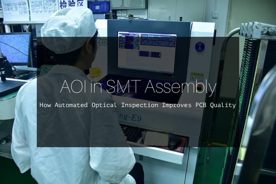
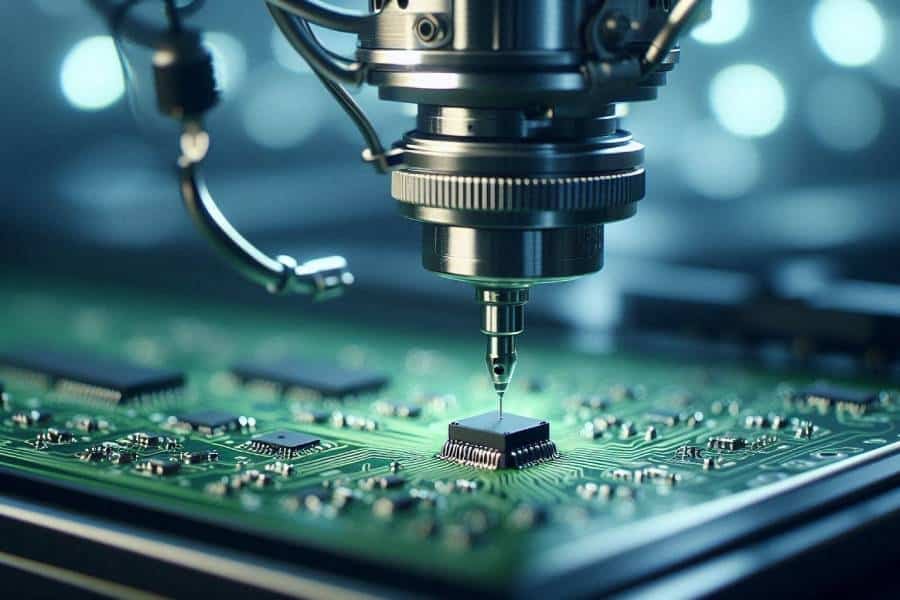
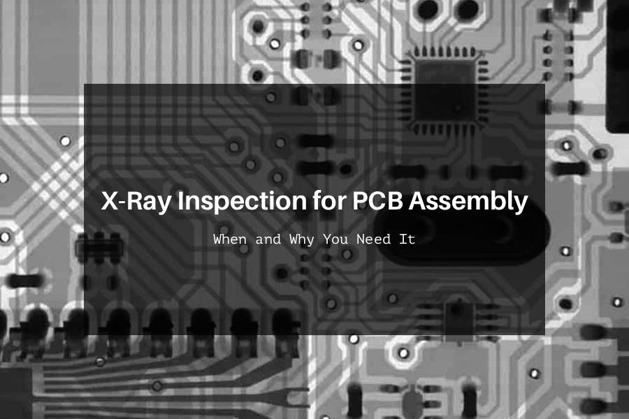
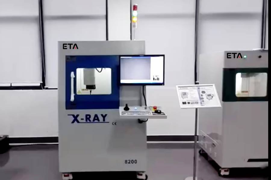
As PCB assemblies become more compact and complex, inspecting only what is visible on the surface is no longer enough to guarantee product reliability. Components such as BGA, QFN, and other hidden-lead packages can develop solder defects that remain completely invisible to the naked eye or even to AOI systems, making X-ray inspection an essential part of modern PCB assembly quality control.
X-ray inspection gives manufacturers a non-destructive way to evaluate internal solder joints, detect voids, bridging, open connections, and other hidden defects that can compromise long-term performance. For high-density assemblies and high-reliability applications, this level of visibility is critical because it helps prevent latent failures before boards leave the factory.
At JHYPCB, we treat X-ray inspection as a key complement to AOI rather than a replacement for it. AOI is ideal for surface-level defect detection, while X-ray provides the deeper insight needed to verify concealed solder joints and support a more complete inspection strategy for demanding PCB projects.
What Is X-Ray Inspection in PCB Assembly?
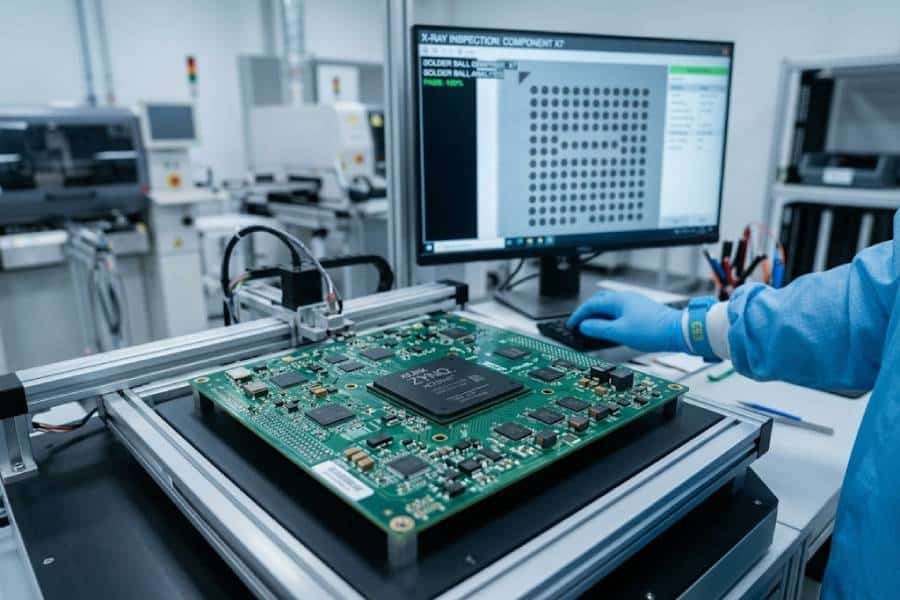
X-Ray inspection in PCB assembly is a non-destructive testing method that uses X-ray imaging to reveal defects hidden beneath components or inside solder joints.
Unlike AOI, which relies on visible light and only inspects what can be seen on the surface, X-Ray can penetrate packages such as BGA, QFN, LGA, and CSP to expose internal connection quality.
This makes X-Ray especially valuable when the most critical solder joints are completely invisible after reflow.
In practice, the system captures internal images of the board so engineers can evaluate solder integrity, alignment, and structural issues without cutting open or damaging the assembly.
How It Works
An X-Ray inspection system typically includes an X-ray source, a detector, a sample stage, and analysis software.
The source emits X-rays through the PCB, and the detector captures the attenuation differences created by materials of different densities, producing a digital image of the internal structure.
Because solder, copper, and air absorb X-rays differently, defects such as voids, cracks, missing solder, or bridging become visible in the image.
This allows inspectors to detect problems that would otherwise remain hidden until failure in the field.
2D and 3D Inspection
In PCB assembly, 2D X-Ray inspection is commonly used for fast evaluation of solder joints and hidden packages.
It is especially useful for routine production checks because it is efficient and widely applicable to BGA and QFN inspection.
For more complex boards or deeper failure analysis, 3D X-Ray methods such as CT provide additional depth information and a clearer view of internal structures.
That extra visibility can be important when the goal is not just to find a defect, but to understand its exact shape, location, and severity.
Where It Fits in Quality Control
X-Ray inspection is not a replacement for AOI; it fills a different role in the inspection chain.
AOI is ideal for surface-level defects, while X-Ray is the better choice when the quality risk is buried under the component or inside the board itself.
For that reason, many manufacturers use AOI and X-Ray together as part of a layered quality control strategy.
This combined approach is especially important for high-density, high-reliability PCB assemblies where hidden solder joint failures can be costly and difficult to diagnose later.
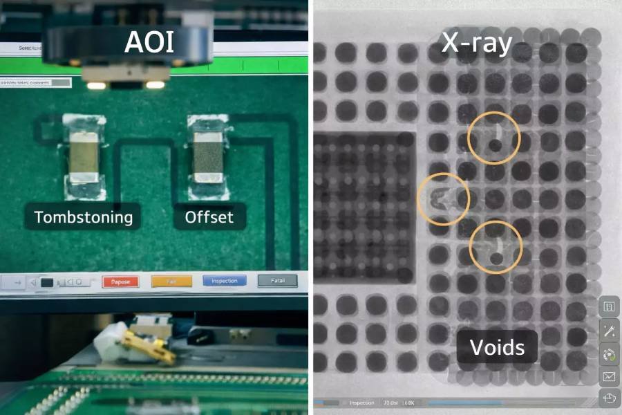
Why AOI Cannot Detect Hidden Joints
AOI is extremely effective for surface-level inspection, but it is limited by one fundamental constraint: it can only inspect what light can reach. When a solder joint is hidden beneath a component body, such as in BGA, QFN, or LGA packages, AOI cannot verify the joint itself because the package physically blocks the line of sight.
This limitation becomes more important as PCB assemblies move toward smaller pitches and higher component density. In these designs, a growing share of critical solder connections sits underneath the package rather than beside it, which means optical inspection can confirm placement and orientation but not the quality of the hidden interconnects.
AOI also cannot evaluate internal solder conditions such as voids, hidden bridges, insufficient wetting, or head-in-pillow defects under the component body. These issues may not be visible from any angle, even with advanced lighting, because photons cannot penetrate dense materials like solder, silicon, and package substrates in a way that reveals the joint structure underneath.
That is why AOI and X-Ray serve different purposes in PCB assembly quality control. AOI is the right tool for exposed features on the board surface, while X-Ray is the proper method for inspecting concealed solder joints and other subsurface defects that would otherwise remain undetected until failure.
What Defects X-Ray Can Reveal
X-Ray inspection is most valuable when the defect is hidden inside the solder joint rather than visible on the surface.
It can expose problems that often survive initial electrical checks but later lead to intermittent failure, thermal stress issues, or long-term reliability loss.
One of the most common issues X-Ray reveals is solder voiding. Voids appear as low-density gaps inside the solder and can weaken both thermal transfer and mechanical strength, especially when they occupy a significant portion of the joint area.
This is particularly important in high-power or high-reliability designs, where excess voiding can reduce performance over time.
X-Ray is also highly effective at detecting solder bridging beneath packages such as BGA and QFN.
Because the bridge is hidden under the component, it may not be visible to AOI, but X-Ray can show unintended solder connections between adjacent pads or balls before the board is shipped.
Another critical defect is the open joint or missing connection, where the solder ball does not properly form a conductive path.
These opens can be especially dangerous because the board may look acceptable externally while still containing an unreliable or incomplete hidden connection.
X-Ray can also help identify head-in-pillow (HIP) defects, where the solder ball and paste fail to fully coalesce during reflow.
HIP defects are often intermittent and may pass basic checks, but X-Ray helps reveal the separation or weak bonding pattern that signals a latent reliability problem.
In addition, X-Ray can uncover insufficient solder fill, misalignment, and internal structural anomalies that affect package integrity.
For this reason, X-Ray is not just a defect-detection tool; it is also an essential method for quality engineers who need to diagnose root causes and improve process control.
When X-Ray Inspection Is Required
X-Ray inspection is required whenever the most important solder connections cannot be verified from the surface.
In practical terms, that means it becomes essential for assemblies using BGA, Micro-BGA, QFN, LGA, CSP, and flip-chip packages, where critical joints sit beneath the component body and cannot be fully checked by AOI.
It is also strongly recommended for high-reliability products, especially in automotive, medical, industrial, and aerospace applications.
In these markets, hidden solder defects can lead to intermittent faults, field failures, or costly recalls, so X-Ray is often used as part of a stricter inspection workflow.
X-Ray inspection is especially useful after reflow when the board includes dense or high-value components that are difficult to rework.
This gives the manufacturer a chance to confirm solder integrity before the board moves into final test, shipment, or system integration.
Another common trigger is when AOI results are inconclusive or when a board has a history of unexplained failures.
In those cases, X-Ray acts as a deeper diagnostic tool that helps engineers pinpoint whether the problem is voiding, bridging, incomplete wetting, or another hidden defect.
For many projects, the decision is simple: if the design includes hidden joints, X-Ray is not optional; it is a required part of quality control.
That is why manufacturers often combine AOI and X-Ray as a layered inspection strategy rather than relying on one method alone.
How X-Ray Inspection Improves PCB Assembly Quality
X-Ray inspection improves PCB assembly quality by giving engineers visibility into solder joints and structures that cannot be checked with optical methods.
That extra visibility helps manufacturers catch hidden defects earlier, before they become field failures, rework loops, or scrap losses.
One of the biggest benefits is early defect detection. When voids, bridges, opens, or insufficient solder are identified soon after reflow, the team can stop process drift before more boards are affected.
This is especially valuable in high-volume production, where even a small recurring defect can multiply quickly across a batch.
X-Ray inspection also strengthens process control. The images and measurements it provides help engineers trace defects back to upstream causes such as stencil issues, solder paste volume, placement accuracy, or reflow profile problems.
That means X-Ray is not only a detection tool, but also a feedback tool that supports continuous manufacturing improvement.
It also improves yield and cost efficiency. By reducing the number of hidden defects that escape into later stages, manufacturers can lower rework, minimize scrap, and avoid expensive returns or failures in the field.
For customers, this usually translates into more stable delivery quality and better long-term product reliability.
For complex assemblies, X-Ray inspection is especially important because it supports root cause analysis and helps validate whether a rework or process adjustment actually solved the issue.
That makes it a practical quality-control step for high-density boards, prototype rework, and projects where hidden solder integrity is critical.
X-Ray vs. AOI vs. ICT/FCT
X-Ray, AOI, and ICT/FCT solve different quality problems, so the best strategy is usually to combine them rather than choose only one.
AOI verifies what is visible on the surface, X-Ray verifies hidden solder structure, ICT verifies electrical connectivity at the component or net level, and FCT verifies whether the assembled board behaves correctly in real use.
A simple way to think about it is this: AOI answers “Did the parts go on correctly?”, X-Ray answers “Are the hidden joints sound?”, ICT answers “Are the circuits electrically correct?”, and FCT answers “Does the product actually work?”.
That layered approach gives much broader coverage than any single test method can provide on its own.
| Method | What it checks | Best use case |
|---|---|---|
| AOI | Surface placement, polarity, visible solder issues | Fast inline SMT inspection |
| X-Ray | Hidden joints, voids, bridges, opens under BGA/QFN/LGA | Dense boards and concealed solder joints |
| ICT | Shorts, opens, component values, electrical integrity | Volume production with fixture planning |
| FCT | Real operating behavior and system functionality | Final product validation |
In practical production terms, AOI is usually the fastest in-line checkpoint, X-Ray is the deeper structural check, ICT is the electrical diagnostic tool, and FCT is the final functional proof.
For boards with BGAs or other hidden connections, X-Ray is the inspection method that closes the gap left by AOI.
For manufacturers and buyers, this comparison matters because it helps match the test strategy to the risk level of the project.
If the design is high-density, high-reliability, or expensive to rework, combining AOI, X-Ray, and electrical testing usually gives the strongest quality assurance outcome.
Partner with JHYPCB for Reliable PCB Inspection
At JHYPCB, we understand that inspection is not just a final checkpoint — it is a critical part of building reliable PCB assemblies. From AOI to X-Ray and beyond, our inspection workflow is designed to help customers catch hidden defects early, improve process control, and deliver boards that meet demanding quality expectations.
For projects involving BGA, QFN, high-density layouts, or other complex assemblies, a single inspection method is rarely enough. That is why JHYPCB combines multiple quality control methods to create a more complete inspection strategy, helping customers reduce risk, improve consistency, and support long-term product reliability.
If your project requires dependable SMT PCB assembly with stronger inspection coverage, JHYPCB is ready to help. Our team can recommend the right balance of AOI, X-Ray, ICT, and functional testing based on your design, volume, and reliability requirements, so you can move forward with greater confidence.
Need a reliable SMT PCB assembly partner? Contact JHYPCB to discuss your project requirements and quality control needs.