Nano-Coated PCB Stencil Manufacturing for Precision & Durability
Discover the next level of precision with our nano-coated PCB stencils. Specially designed to support your high-precision SMT needs, our nano-coating treatment enhances stencil durability, boosts print quality, and reduces maintenance—all to make your production smoother and more efficient.
Ready to take your manufacturing process to the next level? Let us help you achieve unmatched precision with nano-coating technology. Scroll down to learn more, or reach out to see how JHYPCB can meet your unique requirements.
Why Choose Nano-Coated PCB Stencils for Your SMT Needs?
Imagine having a stencil that not only delivers precise results but also lasts longer and requires less frequent cleaning. That’s exactly what nano-coated PCB stencils bring to the table. At JHYPCB, we understand the high standards of surface-mount technology (SMT) manufacturing and know that even small improvements in stencil performance can make a huge difference in your production line.
Our nano-coating treatment creates a super-smooth, non-stick surface on the stencil, significantly reducing solder paste residue and ensuring each print is crisp and accurate. For you, that means less downtime, more consistent prints, and a simplified cleaning process—all translating into higher efficiency and better product quality.
Whether you’re working with complex multilayer PCBs or tackling high-density designs, our nano-coated stencils offer the reliability and precision you need. By choosing JHYPCB, you’re partnering with a team dedicated to helping you streamline your production and improve every print.

Unleash the Benefits of Nano-Coated PCB Stencils
Choosing a nano-coated stencil means choosing reliability, efficiency, and quality. Here’s how our nano-coating technology enhances your PCB production process:
- Exceptional Print Accuracy
Tired of dealing with smudged or inconsistent prints? Our nano-coating creates a super-smooth, non-stick stencil surface that keeps solder paste precisely where it’s meant to be. This level of precision is perfect for high-density and complex PCB designs, ensuring each print meets the highest standards. - Reduced Maintenance, Less Downtime
Say goodbye to frequent stencil cleaning sessions! With nano-coated stencils, solder paste buildup is minimized, which means less time spent on maintenance and more time on production. Fewer cleaning cycles not only streamline your workflow but also extend the stencil’s lifespan. - Enhanced Durability for Long-Lasting Performance
Stencils go through a lot on the production line, and our nano-coating adds an extra layer of protection, reducing wear and tear. You get a stencil that not only performs better but also lasts longer, saving on replacement costs in the long run.
Each of these benefits supports a smoother, more efficient production process. When you choose JHYPCB’s nano-coated stencils, you’re investing in quality, durability, and precision to elevate your SMT manufacturing.


Perfect for High-Demand Industries and Complex Applications
JHYPCB’s nano-coated stencils are designed to meet the precision needs of a wide range of industries. Wherever reliability and fine detail are paramount, our stencils offer unmatched performance:
Consumer Electronics
From smartphones to tablets, consumer electronics require high-density, miniature PCBs that leave no room for error. Our nano-coated stencils ensure every print is sharp, contributing to seamless assembly and device functionality.
Automotive Electronics
Automotive systems demand durability and precision, from sensors to control units. Our stencils are built to withstand the high-volume production needed in automotive manufacturing, providing consistent, high-quality prints that last.
Medical Devices
In the medical field, accuracy is critical. Our nano-coating technology ensures that medical PCBs—used in devices such as diagnostic equipment and monitoring tools—are printed with the precision necessary for reliable performance.
Telecommunications
With the rapid advancements in telecommunications, high-frequency PCB designs are becoming increasingly complex. Our nano-coated stencils provide the precision needed for the exacting standards of telecom applications, helping you stay ahead in a fast-evolving industry.
Whether you’re in high-tech manufacturing, automotive, or medical technology, our nano-coated stencils are crafted to support precision and consistency, no matter how complex your applications.
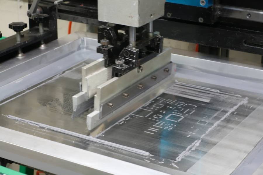
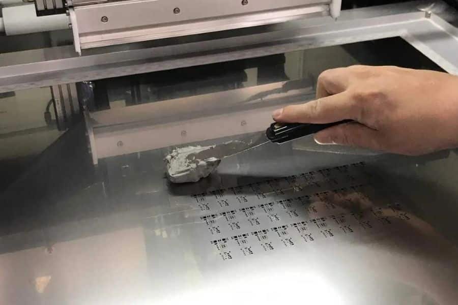
How Our Nano-Coated Stencils Are Made: Precision in Every Step
Producing high-quality nano-coated stencils requires a meticulous process that ensures reliability and durability. Here’s a look at the key steps involved:
Material Selection
We start by selecting premium stainless steel for its durability and consistency. This choice of material is essential for achieving a stencil that can withstand high-volume production and offer precise, clean prints over time.Laser Cutting
Once the material is prepared, we use advanced laser cutting technology to achieve extremely accurate apertures. This precision cutting enables our stencils to deliver sharp, detailed prints, even for high-density and complex PCB designs.Nano Coating Application
After laser cutting, the stencil undergoes a nano-coating process. This specialized coating creates a smooth, non-stick surface that minimizes solder paste buildup, reduces the need for frequent cleaning, and prolongs the stencil’s lifespan.
Each step in our production process is designed to enhance stencil performance, ensuring that our nano-coated stencils meet the high standards required in SMT manufacturing.
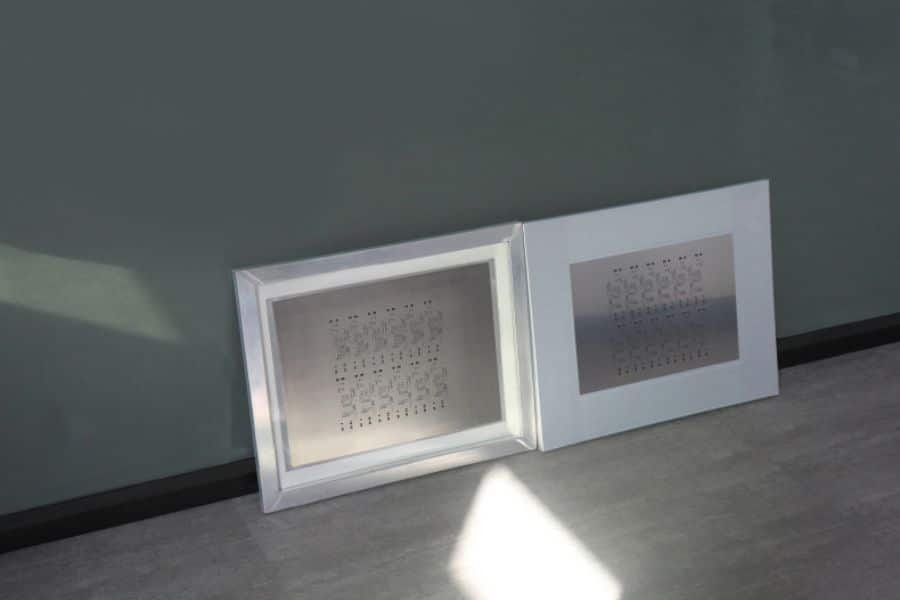
Types of Nano-Coated Stencils
JHYPCB provides a range of nano-coated stencils tailored to meet different application needs in SMT manufacturing. Understanding each type can help you choose the best stencil for your specific requirements:
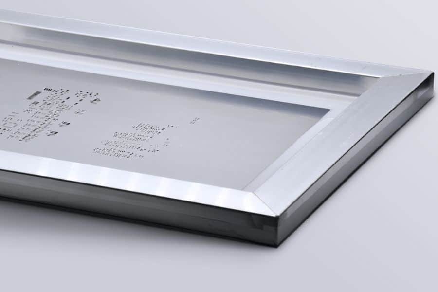
Frameless and Framed Stencils
- Frameless Stencils: These stencils are designed to be flexible and cost-effective, ideal for prototyping or small-volume runs where frequent stencil changes are necessary. They are compatible with a universal frame, making them easy to replace and store.
- Framed Stencils: With a sturdy frame for better alignment and stability, framed stencils are suitable for high-volume production where consistency and durability are essential. They reduce misalignment issues, ensuring precise, repeatable results.
Step Stencils
For complex assembly processes that require varying solder paste thicknesses, step stencils are the ideal choice. These stencils feature multiple thickness levels within a single stencil, enabling accurate solder deposition for components with different height requirements. This makes them highly suitable for intricate PCB designs that involve mixed technology.Electroformed Stencils
Designed for ultra-high precision applications, electroformed stencils are made through an electroforming process, providing smooth and highly accurate apertures. These stencils are perfect for extremely fine-pitch components and applications requiring meticulous precision, such as microelectronics.
Choosing the right type of stencil for your application can enhance production efficiency, reduce errors, and improve end-product quality. Our team is here to guide you in selecting the ideal stencil type for your unique requirements.”


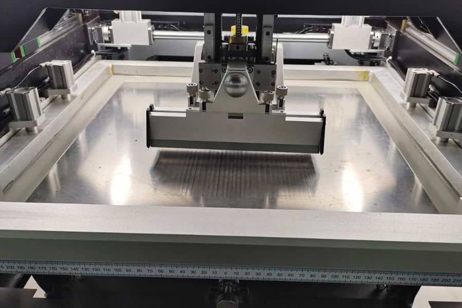
Quality Assurance and Inspection: Ensuring Precision Every Step of the Way
At JHYPCB, quality isn’t just a standard—it’s a commitment. Every nano-coated stencil we produce goes through a meticulous quality control process to ensure it meets the exacting standards of our clients and the demands of high-precision SMT applications.
Strict Quality Control Standards
From the initial material selection to the final nano-coating application, we follow a series of strict quality control protocols. Each stencil is inspected for dimensional accuracy, smoothness of the apertures, and coating consistency, ensuring that every piece performs flawlessly in high-precision PCB assembly.
Advanced Inspection Techniques
Our inspection process includes the use of advanced measurement tools and high-resolution imaging equipment to verify that each stencil meets industry specifications. We check for exact aperture sizes, alignment accuracy, and nano-coating uniformity to guarantee that our stencils deliver consistent, clean solder paste applications.
Our dedication to quality assurance and rigorous inspection protocols mean you can rely on JHYPCB’s nano-coated stencils to deliver precision, durability, and the performance you need in high-stakes applications. Our team is always ready to provide further testing or certification upon request, helping you meet even the most stringent quality demands.
Frequently Asked Questions: Get the Answers You Need
At JHYPCB, we understand that clarity is key when it comes to making decisions about your nano-coated stencils. To help you get the most out of your experience with us, we’ve compiled answers to some of the most common questions our customers ask. If you don’t see the answer you’re looking for, feel free to contact us directly!
The standard lead time for nano-coated stencils typically ranges from 5 to 10 business days, depending on the complexity of your order and the required specifications. If you need a faster turnaround, please reach out to us and we’ll do our best to accommodate your timeline.
Yes, we provide custom-sized stencils to meet your specific needs. Whether you require a non-standard dimension or a special design, we can tailor our stencils to fit your exact specifications.
Our team is here to help guide you! We recommend discussing your project with our experts, who can advise you on the best stencil type based on your specific requirements, such as component size, paste volume, and production volume.
We use a high-quality nano-coating material that enhances the stencils’ durability, improves solder paste release, and reduces the risk of bridging and misalignment. The coating is designed to provide consistent performance in high-precision applications.
Proper care is essential to extending the life of your nano-coated stencils. We recommend following standard cleaning protocols for your stencils, using non-abrasive cleaners to maintain the integrity of the nano-coating. We also provide guidelines for storage and handling to ensure optimal performance over time.
Nano-coated stencils are widely used in industries such as automotive electronics, consumer electronics, and medical devices. These sectors require high precision, and our nano-coated stencils are engineered to meet the demanding standards of these applications.
Request a Quote
* Your quote will be sent directly to JHYPCB and we will reply to you in 2-8 hours.