
RF & Microwave Bare PCB Fabrication
High Frequency PCB Manufacturing
Custom RF and microwave bare PCBs manufactured to your fabrication files, specified materials and stackup requirements. PCBELEC supports Rogers, PTFE-based and hybrid RF + FR-4 constructions from prototype builds to production orders.
Send your board files, operating band and RF requirements to sales@pcbelec.com
- Construction Options Double-Sided, Multilayer & Hybrid
- Engineering Preparation RF Stackup & Fabrication DFM
- Manufacturing Orders Prototypes to Production
RF, Microwave & Mixed RF / Digital Builds
RF & Microwave PCB Fabrication Options
PCBELEC manufactures bare boards for RF signal paths, microwave circuits and mixed RF / digital designs. Define the construction around the specified material, operating band and transmission-line requirements.
-
01
Double-Sided RF PCBs
Two-layer constructions with the circuit pattern and reference conductor defined around the selected RF laminate and dielectric thickness.
Define for Fabrication Material grade, copper, dielectric thickness, reference plane and critical RF geometry.
-
02
Multilayer RF PCBs
Multilayer boards with specified signal layers, reference planes and interlayer connections. Review the complete dielectric and bonding construction with the RF requirements.
Define for Fabrication Released stackup, layer functions, bonding materials and relevant hole or via structures.
-
03
Hybrid RF + FR-4 PCBs
Combine designated RF dielectric layers with FR-4 regions in a defined multilayer construction. Assign the material and electrical requirements to the relevant signal paths and layers.
Define for Fabrication RF core, FR-4 grade, bondply or prepreg, layer interfaces and approved material alternatives.
High Frequency and High-Speed Are Related, Not Identical
RF designs are commonly specified by operating band and frequency-domain behavior. High-speed digital designs also depend on signal transition times and channel requirements. They can share transmission-line and material concerns, but should not be defined by one universal frequency threshold.
RF Board Construction & Critical Features
High Frequency PCB Manufacturing Capabilities
PCBELEC manufactures RF and microwave bare PCBs from the released design and construction requirements. Review the general fabrication range, critical features and special material combinations below.
- Layer Range 2–22 Layers Double-sided, multilayer and defined hybrid RF constructions.
- Board Size Up to 500 × 500 mm Provide the finished outline and required delivery form.
- Controlled Impedance Typical ±10% Define targets, structures and required verification with the order.
A / General Fabrication
Board Construction and Fabrication Range
Swipe horizontally to view the full fabrication table.
| Manufacturing Item | Range / Configuration | Define in Your Package |
|---|---|---|
| Board construction | Rigid RF and microwave PCBs, including specified hybrid RF + FR-4 stackups. | Layer functions, RF regions, material interfaces and intended signal structures. |
| Material systems | Rogers, PTFE-based laminates, specified Taconic grades and suitable FR-4 combinations. | Exact laminate designation, dielectric thickness, copper configuration and permitted alternatives. |
| Layer count | 2–22 layers. | Complete layer order, dielectric construction and relevant interconnect requirements. |
| Board size | Up to 500 × 500 mm. | Finished outline, critical dimensions, tolerances and single-board or panel delivery. |
| Finished thickness | 0.2–4.0 mm. | Overall thickness and tolerance, together with controlled dielectric dimensions where required. |
| Copper thickness | 0.5–3 oz/ft². | Copper by layer, starting or finished basis and specified foil type or profile. |
| Surface finishes | ENIG, OSP, immersion silver and specified hard-gold areas. | Required finish, coverage and any selective contact plating requirements. |
| Production scope | Prototypes, small batches and production orders. | Quantity, design revision, material requirements and target delivery date. |
B / Critical Features and Electrical Requirements
Define the Features That Control Your RF Build
Identify critical conductor and dielectric dimensions explicitly. Keep RF acceptance requirements separate from general board dimensions and basic electrical connectivity.
Swipe horizontally to view all feature and verification details.
| Feature / Requirement | Capability / Reference | Order Definition |
|---|---|---|
| Trace width / spacing | 0.15 mm trace width / 0.13 mm spacing. | State critical finished widths and gaps. Review the layout with copper thickness and material construction. |
| Hole-size reference | 0.20–0.30 mm reference, depending on construction. | Identify whether dimensions are drill-tool or finished-hole sizes. Define hole type, tolerance and the applicable board structure. |
| Controlled impedance | Single-ended and differential; typical tolerance ±10%. | Provide targets, relevant layers, reference planes, structures and required verification. |
| Dielectric and RF geometry | Drawing- and stackup-defined critical characteristics. | Identify dielectric thickness, critical line geometry and features requiring approval before modification. |
| Bare-board electrical test | Continuity and isolation against the agreed test data. | Identify the electrical reference, acceptance requirements and requested test records. |
| RF performance verification | A separately defined project requirement. | Submit any insertion-loss, return-loss or phase criteria, test band, method and specimen requirements for scope confirmation. |
The 500 MHz–20 GHz application band stated for this service is project context, not a claim that every board or material is RF-tested across that band. Electrical connectivity, impedance and RF performance are distinct verification scopes.
C / Special Construction Review
Confirm the Material and Process Combination
Hybrid RF + FR-4
Define the RF core, FR-4 regions and bonding system as one construction. Review dielectric interfaces, copper balance and the relevant layer connections together.
Include for Review Released stackup, material grades, bondply or prepreg and critical electrical structures.
PTFE-Based Builds
Identify the exact laminate and copper configuration. Manufacturing preparation accounts for the material-specific handling, drilling, hole preparation and bonding requirements.
Include for Review Grade, dielectric thickness, hole structures and any special dimensional requirements.
Multilayer Interconnects
Specify blind or buried connections and other controlled interlayer features where required. Identify the layer spans and any filling or capping instructions explicitly.
Include for Review Via map, construction sections, finished-hole requirements and applicable acceptance criteria.
The selected material, stackup, copper and feature geometry form one manufacturing combination. Submit them together so the quotation reflects the actual build.
Manufacturing File Requirements →Laminate, Copper & Bonding-System Definition
RF Materials and Hybrid Stackups
Select the laminate against the operating band, loss budget, transmission-line structure and manufacturing requirements. Specify the exact grade, dielectric thickness and copper configuration instead of relying on a brand or a single Dk number.
Material Directions for RF PCB Fabrication
Swipe horizontally to view the complete material guide.
| Material Direction | Grade Examples | Define for the Actual Build |
|---|---|---|
| Hydrocarbon / ceramic laminates | Rogers RO4350B and RO4003C. | Exact grade, dielectric thickness, applicable Dk / Df basis, copper foil and compatible multilayer bonding construction. |
| Ceramic-filled PTFE laminates | Rogers RO3003 and RO3010. | Grade-specific dielectric properties, thickness and copper options, hole preparation and bonding requirements. |
| Glass-microfiber-reinforced PTFE | Rogers RT/duroid 5880. | Laminate designation, thickness, copper configuration and dimensional or handling requirements for the construction. |
| Other specified RF grades | Taconic RF-35 and specified TLX subgrades. | Full grade designation and current datasheet conditions. A material-family name alone does not define one dielectric constant. |
Specify the exact grade, dielectric thickness and copper configuration. Identify permitted alternatives with the inquiry so the material and construction can be confirmed together. Rogers is a supplier with multiple resin systems; PTFE identifies a material system rather than a brand.
Process Dk and Design Dk Serve Different Purposes
Manufacturer data may distinguish process-control values from recommended design values. For example, Rogers publishes the following for RO4350B:
Design Dk: 3.66
Use the applicable datasheet conditions and modeling basis. Do not treat these values as interchangeable entries in an impedance calculation.
Loss Is More Than a Laminate Df Value
Material loss, conductor geometry, copper profile and discontinuities contribute to the behavior of a fabricated RF path. A low published Df does not establish the insertion loss of the complete board.
Identify the copper foil, finish, mask coverage and critical features that must remain consistent with the design assumptions.
Need a broader comparison of dielectric behavior, copper profile and material construction?
RF & High Frequency PCB Material Guide →Critical RF Features & Manufacturing Definition
RF Stackup and Fabrication DFM
Translate the supplied RF design into a clear manufacturing package. PCBELEC reviews the construction, conductor features and process requirements while keeping customer-controlled RF geometry and approval rules explicit.
-
01
Finished RF Conductor Geometry
Identify transmission-line widths, coupling gaps, antenna features and other critical copper geometry. Review etching and plating effects against the required finished pattern rather than treating every feature as freely adjustable.
Define for Review Critical finished dimensions, tolerances, controlled RF regions and no-change features.
-
02
Dielectric Thickness & Reference Planes
Define the dielectric between each relevant signal layer and its reference conductor. Distinguish core thickness, pressed bonding dielectric and overall board thickness in the released stackup.
Define for Review Layer functions, reference planes, dielectric dimensions and the design Dk basis.
-
03
Copper Foil & Finished Copper
Specify the copper configuration used by the design assumptions. Identify any controlled foil type or surface profile, and distinguish starting foil from finished conductor requirements.
Define for Review Copper by layer, foil designation, relevant roughness specification and finished-thickness basis.
-
04
Solder Mask & Surface Finish
Mark RF traces and features that require mask coverage or intentional exposure. Identify the finish on the relevant conductors and any local or selective plating.
Define for Review Mask boundaries, exposed RF areas, finish coverage and critical registration requirements.
-
05
Grounding Features & Layer Transitions
Preserve the specified positions of ground vias, connector features, slots and interlayer connections. Review their hole, plating and mechanical definitions without assuming that relocating them is electrically neutral.
Define for Review Via spans, finished holes, positional tolerances, connector references and any via treatment.
-
06
Hybrid Bonding & Layer Registration
Review RF cores, bonding materials and FR-4 regions as one construction. Identify resin-fill needs, copper distribution and critical alignment between layers or mechanical features.
Define for Review Complete material stackup, bonding dielectric, alignment requirements and permitted alternatives.
Provide a Consistent Review Package
- Matching artwork, drill data, board outline and drawing revision.
- Material grades, copper and dielectric requirements by layer.
- Operating band, impedance targets and relevant signal structures.
- Critical dimensions and customer-controlled RF features.
Resolve the Manufacturing Definition
- Confirm the intended stackup and material combination.
- Document agreed changes to construction or feature geometry.
- Identify the applicable acceptance criteria and requested verification.
- Release one approved revision for the fabrication order.
This is fabrication-focused review of customer-supplied designs. RF circuit design, antenna tuning, PCB layout and system-level simulation are separate from this manufacturing service.
Manufacturing File Requirements →Bare-Board Acceptance & Defined RF Test Scope
Electrical, Impedance and RF Verification
Match verification to the characteristic you need to control. Electrical connectivity, transmission-line impedance and frequency-dependent RF performance answer different questions and require clearly defined acceptance criteria.
-
01 / Connectivity
Bare-Board Electrical Test
Checks intended connections and isolation between nets against the approved electrical test data.
Are the required connections present without unintended opens or shorts?
-
02 / Transmission-Line Structure
Controlled-Impedance Verification
Evaluates the specified impedance structures using the agreed method and test specimen, where required by the order.
Does the measured structure meet the agreed impedance target and tolerance?
-
03 / Frequency-Domain Performance
Project-Specific RF Measurement
Evaluates defined characteristics such as insertion loss, return loss or phase under specified measurement conditions.
Does the agreed test structure meet the RF criteria across the specified band?
Define the Evidence Required for Your Order
Swipe horizontally to view all verification requirements.
| Verification Area | Review / Inspection Focus | Specify with the Order |
|---|---|---|
| Material and construction | Specified laminate, copper configuration and released stackup, including approved material alternatives. | Exact grade, construction reference and any required material identification or traceability documents. |
| Critical geometry | Drawing-controlled conductors, dielectric dimensions, board features and relevant holes. | Critical dimensions, measurement locations, tolerances and requested dimensional or cross-section records. |
| Continuity and isolation | Intended net connections and separation from unrelated nets. | Approved test-data reference, electrical acceptance requirements and requested test summary. |
| Controlled impedance | Defined transmission-line structures, commonly evaluated using a representative coupon where specified. | Target and tolerance, layer and structure, test method, specimen and required report. |
| RF performance | Project-defined frequency-domain measurements, subject to a separately agreed test scope. | Frequency band, metrics, limits, test structure, measurement reference planes and requested data format. |
Passing continuity or impedance checks does not by itself establish insertion loss, return loss or phase performance. Coupon results apply to the tested structures and conditions; define how they are used in the order's acceptance requirements.
Define requested material, dimensional, electrical and impedance records before production. RF measurements are not included by default; the agreed order specifies the verification scope and deliverables.
Bare PCB Testing & Inspection →Selected Build Examples & Order Continuity
RF PCB Build Examples and Production Support
Explore selected constructions from PCBELEC's published RF PCB examples. Use the material, layer and fabrication details to identify the build requirements relevant to your next prototype or production order.
-
 Double-Sided RF Construction
2-Layer RO4350B RF PCB
- Material
- Rogers RO4350B.
- Layer Count
- 2 layers.
- Finished Board Thickness
- 0.8 ± 0.1 mm.
- Surface Finish
- ENIG.
Relevant Manufacturing DefinitionSpecify the laminate thickness, copper configuration and critical conductor dimensions together with the RF reference structure.
-
Mixed RF / Digital Construction
4-Layer RF + FR-4 Hybrid PCB
- Material Combination
- Rogers RT/duroid 5880 with Shengyi FR-4.
- Layer Count
- 4 layers.
- Finished Board Thickness
- 1.6 ± 0.14 mm.
- Surface Finish
- OSP.
Relevant Manufacturing DefinitionIdentify the exact FR-4 grade, RF layer assignment and bonding system in the released stackup. Do not apply one dielectric value to the complete hybrid board.
-
Specified RF Laminate Construction
2-Layer RF-35 PCB
- Material
- Taconic RF-35.
- Layer Count
- 2 layers.
- Finished Board Thickness
- 0.8 ± 0.1 mm.
- Surface Finish
- ENIG.
Relevant Manufacturing DefinitionKeep the full material designation, dielectric construction and finished geometry consistent with the design requirements and approved alternatives.

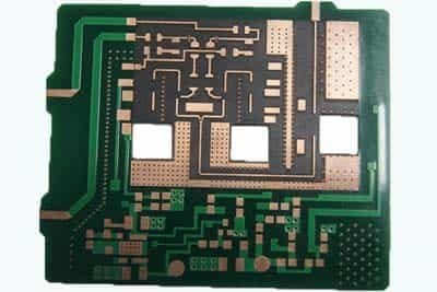

These are individual build references, not universal specifications or RF performance qualification results. Your order uses its own released material, construction and acceptance requirements.
From Prototype Definition to Repeat Production
PCBELEC supports prototype, small-batch and production fabrication. Keep the approved material and stackup identifiable through each stage, and review changes before the next manufacturing release.
-
01 / Review
Share Files and RF Requirements
Provide the artwork, drill data, stackup, operating band, critical features and requested quantity for engineering review.
-
02 / Confirm
Agree the Manufacturing Basis
Confirm the material, construction, acceptance scope, quotation and delivery schedule for the intended build.
-
03 / Fabricate
Manufacture and Verify
Fabricate against the released data and complete the agreed bare-board checks and documentation before shipment.
-
04 / Repeat
Carry Approved Requirements Forward
Reference the approved revision for follow-on orders. Identify changes to laminate, foil, bonding system, geometry or verification requirements.
Include the target quantity and delivery date with your RF fabrication package. Material alternatives and stackup changes follow the agreed approval rules.
RF & Microwave Bare PCB Fabrication Inquiry
Request an RF & Microwave PCB Quote
Send your fabrication files, material and stackup requirements, quantity and target delivery date. PCBELEC reviews the manufacturing definition and critical RF features to prepare a project-specific quotation and delivery schedule.
Include with Your RF PCB Inquiry
- Fabrication Files Gerber files, drill and routing data, board outline, drawing and design revision.
- Materials & Stackup Exact laminate grades, layer order, dielectric thickness, copper configuration and bonding system.
- Operating Band & RF Features Intended frequency band, relevant signal layers, reference planes and critical conductor geometry.
- Impedance & Verification Targets, tolerances, test structures and requested electrical, impedance or additional RF verification.
- Finish & Special Requirements Surface finish, exposed RF regions, hole structures, acceptance criteria and required records.
- Quantity & Delivery Prototype or production quantity, required delivery date, destination and previous order reference, if applicable.
Send Your RF PCB Requirements
Use the form below to share your contact details, project specifications and available files. Identify any proposed material alternatives or requirements that still need confirmation.
Upload your fabrication files, stackup and supporting drawings. You may also email your package to sales@pcbelec.com.
RF Materials, Manufacturing & Ordering
High Frequency PCB FAQ
Answers to common questions about RF laminate selection, hybrid constructions, verification and bare-board manufacturing orders.
Preparing an RF build? Include the material, stackup, operating band and critical manufacturing requirements with your board files.
View the RF Quotation Checklist →Can I use FR-4 for an RF PCB, or do I need a dedicated RF laminate?
FR-4 may be suitable when the actual material, path length and construction meet the design requirements. Frequency alone does not establish a universal material selection threshold.
Review dielectric behavior, loss budget, phase requirements, copper configuration and manufacturing consistency. Specify a dedicated RF laminate where those requirements call for it.
Can PCBELEC manufacture hybrid Rogers + FR-4 PCBs?
Yes. PCBELEC supports specified hybrid RF + FR-4 constructions. Define the RF core, FR-4 grade, bonding material and layer order as one manufacturing stackup.
Identify the RF signal layers, reference planes, critical dielectric dimensions and any changes that require approval.
Which Dk value should I use for an RF stackup or impedance specification?
Use the material-data and modeling basis applicable to the design. A manufacturer may publish process-control Dk and design Dk values for different purposes.
State the laminate grade, relevant frequency or test conditions and the design assumptions in the stackup. Do not substitute one published value for another without reviewing its meaning.
Does passing impedance testing prove that RF insertion loss is acceptable?
No. Impedance verification and insertion-loss measurement evaluate different characteristics. A compliant impedance result does not by itself establish loss, return loss or phase performance across the operating band.
Include any required RF measurement specification with the inquiry. Test structures, conditions, acceptance limits and deliverables are agreed separately from basic electrical testing.
Can a similar RF laminate replace the material in my design?
Not automatically. A similar nominal Dk or material-family description does not establish equivalent loss, copper profile, thickness options or processing behavior.
Identify permitted alternatives and approval rules. Review any proposed change against the complete material, stackup and electrical requirements before release.
Do you provide RF circuit design, PCB layout or antenna tuning?
This service covers bare PCB fabrication and manufacturing-focused review of customer-supplied designs. The review addresses the material, stackup, geometry and fabrication requirements.
RF circuit design, PCB layout, antenna tuning and system-level simulation are separate from this manufacturing service.
What affects RF PCB cost and manufacturing lead time?
Key factors include the exact laminate, material availability, board area, layer count, bonding system, hole structures, critical tolerances, finish and quantity.
Additional verification and documentation can also affect the order scope. Submit the files and target delivery date so pricing and schedule reflect the actual build.
What should I send for an RF or microwave PCB quotation?
Send the fabrication files, drill data, board outline, drawing and stackup with the quantity, design revision and target delivery date.
Include the exact materials, operating band, impedance requirements, critical RF geometry and requested inspection records. Identify any open specifications or proposed alternatives.
How do I keep the RF construction consistent from prototype to production?
Carry the approved material grade, copper configuration, dielectric and bonding construction into the production release. Keep the artwork, drawing and stackup on one matching revision.
Identify changes to material, foil, geometry or verification requirements before the next order. A previous prototype does not automatically approve a later substitution or construction change.