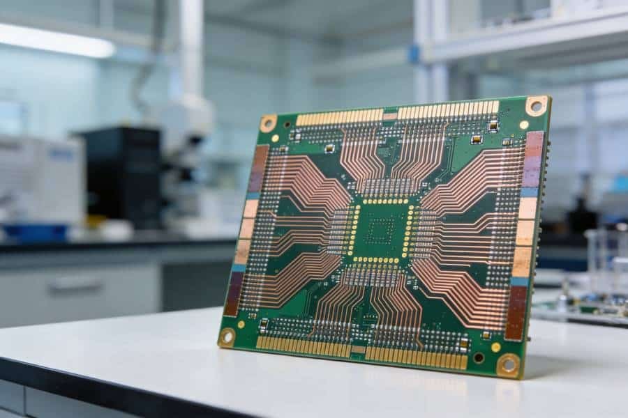
PCB Materials / Ceramic Substrates
Ceramic PCB Materials: Substrate Systems and Fabrication Requirements
Define more than the ceramic name. Understand how substrate grade, metallization, ceramic thickness and conductor requirements fit together when preparing specifications for fabrication review.
- Substrate grade
- Metallization route
- Fabrication specifications
What Is a Ceramic PCB Material System?
A ceramic circuit specification combines an insulating substrate with a defined conductor structure. The ceramic material, the metallization route and the finished circuit requirements need to be identified separately.
01 / Substrate
The Ceramic Base
The base material establishes the starting point for thermal, electrical and mechanical properties. A material family alone does not identify the required grade or finished dimensions.
- Material family and supplier grade
- Ceramic thickness and tolerance
- Material data and test conditions
02 / Metallization
The Conductor Structure
The metallization route defines how conductive features are formed on or joined to the ceramic. It must be considered together with the substrate and conductor requirements.
- Bonded, brazed, plated or printed conductors
- Conductor material and thickness
- Single-sided or double-sided construction
03 / Finished Circuit
The Fabrication Specification
The finished circuit definition turns the material system into a manufacturable part with documented geometry, interfaces and acceptance requirements.
- Circuit pattern, holes and outline
- Surface finish and critical dimensions
- Inspection criteria and required documentation
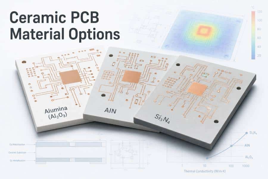
Alumina, Aluminum Nitride and Silicon Nitride Substrates
These ceramic families provide different starting points for a circuit structure. Specify the required material grade and construction rather than treating the family name as a finished product specification.
Swipe or scroll horizontally to view all columns.
| Substrate | Material Direction | What to Specify | What to Confirm |
|---|---|---|---|
| Alumina Al₂O₃ | An established electrically insulating ceramic used in metallized substrates and ceramic circuit structures. | Alumina content or supplier grade, ceramic thickness, surface requirements and the proposed metallization route. | Grade-specific properties, dimensional tolerances and compatibility with the required conductor structure. |
| Aluminum Nitride AlN | A thermally conductive, electrically insulating ceramic evaluated where heat transfer through the substrate is an important requirement. | Supplier grade, required thermal property data and test conditions, ceramic thickness and conductor construction. | The selected grade's data, process compatibility and thermal-mechanical requirements for the complete structure. |
| Silicon Nitride Si₃N₄ | A ceramic considered for metallized power substrates where mechanical robustness and thermal-cycling performance are important. | Supplier grade, ceramic thickness, joining route, conductor thickness and required qualification criteria. | Compatibility of the ceramic and joining process, plus reliability evidence relevant to the specified construction. |
Ceramic Metallization and Circuit Construction
The same ceramic family can be used in different circuit constructions. Identify how the conductors are formed or joined, then review the substrate, conductor dimensions and finished-part requirements as one defined structure.
DBC — Direct Bonded Copper
DBC uses a high-temperature bonding process to join copper to a compatible ceramic substrate. Specify the ceramic and copper layers together, including the required construction on each side.
Specification checkpoints
- Ceramic grade and bonding compatibility
- Copper thickness on each side
- Pattern, edge and dimensional requirements
AMB — Active Metal Brazing
AMB uses an active-metal-containing braze to join copper to ceramic. It is a distinct joining route and is used in silicon nitride power-substrate constructions.
Specification checkpoints
- Ceramic grade and joining system
- Copper and interface requirements
- Construction-specific qualification criteria
DPC — Direct Plated Copper
DPC forms a deposited adhesion and seed structure on the ceramic, followed by copper plating and pattern definition. Any through-hole metallization must be reviewed for the selected process.
Specification checkpoints
- Metallization stack and copper thickness
- Line, space and dimensional tolerances
- Hole geometry and electrical interconnections
Thick-Film Ceramic Circuits
Thick-film construction uses printed pastes that are fired onto a compatible ceramic substrate. The conductor material and fired-film properties must be specified rather than assumed to match a copper-sheet construction.
Specification checkpoints
- Substrate and paste-system compatibility
- Conductor material and fired-film requirements
- Pattern tolerances and terminal requirements
The technologies above describe ceramic circuit construction categories, not a list of PCBELEC production capabilities. Material availability, process support and manufacturing limits must be confirmed for the specific project before quotation or fabrication.
Ceramic Thickness, Conductor Thickness and Material Grade
Define the individual layers before specifying the finished part. Ceramic thickness, conductor thickness and material grade describe different requirements and should be documented separately.
Swipe or scroll horizontally to view all columns.
| Specification Item | What the Customer Should Define | What the Fabrication Review Should Clarify |
|---|---|---|
| Ceramic Material Grade | Material family, supplier grade or governing material specification, including the applicable data sheet revision. | Whether the specified grade can be sourced and processed through the proposed construction route. |
| Ceramic Thickness | Nominal ceramic thickness and tolerance, stated separately from conductor layers and finished-part thickness. | Available substrate thickness, tolerance basis and compatibility with the required outline, holes and metallization. |
| Top-Side Conductor | Conductor material, thickness and tolerance. Identify whether the requirement applies to the starting metal or the finished conductor after processing. | How the selected process achieves and verifies the specified conductor thickness and pattern dimensions. |
| Bottom-Side Conductor | State whether the bottom side is bare, patterned or continuously metallized. Specify its conductor material and thickness independently. | Compatibility of the top and bottom constructions, including any specified flatness or bow requirements. |
| Joining or Metallization Stack | Required construction route and any controlled interface, adhesion, seed or joining layers relevant to the specification. | Whether the requested stack is compatible with the ceramic, conductor system and fabrication sequence. |
| Surface Finish | Finish type, applicable areas and any specified thickness, cleanliness or terminal requirements. | Finish compatibility with the conductor structure and the required inspection or documentation. |
| Finished-Part Thickness | Total thickness and tolerance where functionally necessary, with a clear definition of the included layers and measurement location. | Whether the finished thickness requirement is consistent with the layer specifications and measurement method. |
How to Read Ceramic Substrate Material Data
A useful material comparison includes more than a property value. Check the grade, test conditions and reporting basis before using supplier data in a fabrication specification.
01 / Heat Transfer
Thermal Conductivity
Thermal conductivity describes the ceramic material, not the thermal resistance of the complete circuit or its cooling interface.
Check the data sheet for
- Material grade and measurement temperature
- Test method and units
- Typical values versus specified minimums
02 / Dimensional Change
Thermal Expansion
A coefficient of thermal expansion value must be read with its temperature range. Ceramic data alone does not describe the behavior of a complete metallized structure.
Check the data sheet for
- Temperature interval and reporting basis
- Measurement direction, where relevant
- Whether the value refers to ceramic or a composite
03 / Insulation
Dielectric and Resistivity Data
Dielectric strength and resistivity describe different insulation properties. Neither should be treated as a finished circuit's operating-voltage approval.
Check the data sheet for
- Specimen thickness and electrode arrangement
- Test voltage, duration and environmental conditions
- Applicable product-level acceptance requirements
04 / Mechanical Behavior
Strength and Fracture Toughness
Bending strength and fracture toughness are different measures. A material test result is not a guaranteed load rating for a patterned part with holes or mounting features.
Check the data sheet for
- Test method and specimen geometry
- Surface condition and test temperature
- Relevance to the specified finished-part geometry
05 / Frequency Behavior
Dielectric Constant and Loss
Permittivity and dielectric loss need a stated frequency and test method. Values measured under different conditions may not support a direct comparison.
Check the data sheet for
- Measurement frequency and temperature
- Test method and reported loss parameter
- Grade-specific data for the customer's application
06 / Specification Control
Typical Values and Acceptance Limits
Typical properties provide reference information. A controlled acceptance requirement needs an agreed limit, verification basis and applicable document revision.
Check the specification for
- Minimum, maximum or nominal requirements
- Required evidence or inspection method
- Data sheet revision and substitution approval
Thermal Path, Electrical Isolation and Mechanical Interfaces
Material properties are only one part of the finished structure. Translate the customer's thermal, electrical and mechanical requirements into controlled dimensions, interfaces and acceptance criteria for fabrication review.
01 / Thermal Interface
Define the Complete Heat Path
Ceramic conductivity alone does not establish device temperature or system thermal performance. Ceramic thickness, conductor geometry and the interface to the cooling structure are separate parts of the heat path.
Document for fabrication review
- Ceramic and conductor layer requirements
- Bottom-side metallization and contact geometry
- Specified flatness and interface surface requirements
02 / Electrical Interface
Separate Insulation From Spacing
Insulation through the ceramic, creepage along a surface and clearance through air are different requirements. A ceramic material property does not automatically establish compliant conductor spacing.
Document for fabrication review
- Customer-defined conductor spacing and edge setbacks
- Applicable insulation and safety requirements
- Required electrical tests and acceptance criteria
03 / Mechanical Interface
Control Geometry and Contact Surfaces
Material strength alone does not define the behavior of a finished part. Holes, cutouts, edges and mounting contacts need clear geometry and tolerances in the customer drawing.
Document for fabrication review
- Outline, hole positions and critical dimensions
- Specified edge condition, flatness and bow limits
- Contact areas and mechanically critical features
Need an Application-Focused Material Comparison?
For thermal, mechanical and cost tradeoffs between alumina, aluminum nitride and silicon nitride in high-power electronics, continue with our ceramic substrate selection guide.
Manufacturing Compatibility and Critical Features
A ceramic material choice does not establish the manufacturing rules for the finished circuit. Review critical features against the selected substrate, conductor structure and fabrication route.
01 / Circuit Geometry
Conductor Patterns and Clearances
Pattern requirements need to be reviewed together with conductor thickness and the selected metallization process. Do not carry over design rules from a different construction without confirmation.
- Specify line widths, spaces and dimensional tolerances.
- Identify conductor-to-edge and conductor-to-hole clearances.
- Mark electrically or mechanically critical pattern features.
02 / Holes and Outline
Hole Functions and Edge Features
Mechanical holes and electrical interconnections serve different purposes. State whether each hole is unmetalized, metallized or subject to another defined construction requirement.
- Define hole size, position, tolerance and intended function.
- Document cutouts, slots and critical outline geometry.
- Specify relevant edge-quality and local clearance requirements.
03 / Surfaces and Dimensions
Finished-Part Interfaces
Contact surfaces and critical dimensions require a clear measurement basis. Identify the controlled condition rather than relying on a general request for a flat or smooth part.
- Provide datums and tolerances for critical dimensions.
- Define flatness or bow requirements and measurement conditions.
- Identify finish coverage and any controlled contact areas.
04 / Verification
Inspection and Acceptance Criteria
Acceptance requirements should identify what must be checked, how results are evaluated and which records are required. Material properties and finished-part inspection are not interchangeable.
- State visual, dimensional and electrical acceptance criteria.
- Identify required reports, certificates and traceability.
- Confirm any special testing separately in the quotation scope.
How to Specify Ceramic PCB Materials for Quotation
Prepare a controlled fabrication package that identifies the material, construction and acceptance requirements. Use the checklist below to separate confirmed specifications from items that still need review.
Swipe or scroll horizontally to view all columns.
| RFQ Item | Information to Provide | Clarification Needed |
|---|---|---|
| Part Identification | Part number, drawing revision, material specification revision and an inventory of the files included in the package. | Confirm that all files describe the same controlled revision. |
| Ceramic Material | Required material family, supplier grade or governing material specification, with the relevant data sheet. | Identify whether an exact grade is mandatory or alternatives may be proposed for customer approval. |
| Circuit Construction | Required metallization or joining route and a clearly labeled top-to-bottom construction drawing. | Flag any undecided construction requirement rather than leaving it to an unstated assumption. |
| Layer Thicknesses | Ceramic thickness, conductor material and thickness on each side, applicable tolerances and any controlled total thickness. | Distinguish starting material dimensions from finished dimensions where this affects acceptance. |
| Circuit and Mechanical Files | Circuit artwork, fabrication drawing, outline, hole information and any necessary mechanical definition in agreed file formats. | State units, layer orientation, datums and the controlling source for each critical requirement. |
| Critical Features | Controlled lines and spaces, hole functions, clearances, edge conditions and critical dimensional tolerances. | Identify which features need specific measurement or documented review. |
| Surface and Interface Requirements | Surface finish, finish coverage, specified contact areas, cleanliness and any flatness or bow requirements. | Include applicable limits and measurement conditions instead of general descriptive terms alone. |
| Inspection and Documentation | Visual, dimensional and electrical acceptance requirements, plus requested certificates, reports and traceability. | Confirm which records and verification activities can be included in the quotation. |
| Special Qualification | Any project-specific reliability or qualification requirement, including the governing procedure and acceptance criteria. | Establish responsibility, sample quantity and verification scope separately from routine part inspection. |
| Quantity and Schedule | Requested prototype or production quantities, delivery destination and target delivery date. | Confirm the achievable schedule after material sourcing, process and documentation requirements are reviewed. |
When a Ceramic Substrate Is Not Necessary
Ceramic is one material route, not a universal upgrade. Before committing to it, check whether another construction can meet the customer's validated electrical, thermal and mechanical requirements. Explore the PCB materials guide for the broader material categories.
01 / Existing Requirements
Keep FR-4 Where It Meets the Specification
If a qualified FR-4 construction already meets the project's performance and reliability requirements, a ceramic substitution needs a specific justification rather than a general preference for higher material thermal conductivity.
Identify the unmet requirement first. Do not assume a change in substrate alone will resolve a system-level limitation.
Related material: FR-4 PCB Material
02 / Thermal Management
Evaluate an Insulated Metal Substrate
An aluminum- or copper-based insulated metal substrate may be a candidate where heat transfer is a primary concern. Evaluate the insulating dielectric, its thickness and the complete interface to the cooling structure.
Metal-core conductivity alone is not a measure of the circuit's through-thickness thermal performance or electrical isolation.
Related materials: Aluminum PCB Material · Copper Core PCB Material
03 / High-Frequency Performance
Consider a Qualified RF Laminate
A high-frequency requirement does not automatically call for a solid ceramic substrate. Compare the required dielectric properties, losses, copper characteristics and circuit construction before selecting the material system.
Ceramic-filled polymer laminates are a separate material category from sintered ceramic substrates.
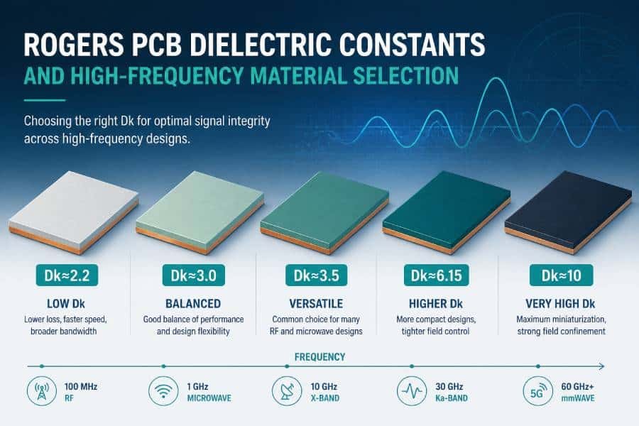
Related material: Rogers PCB Materials
04 / Defined Failure Mode
Match the Material Change to the Actual Problem
A higher thermal rating or a different material label does not automatically solve electrical loss, interface resistance, mechanical loading or long-term reliability.
The customer design team should identify the limiting condition and validate the proposed alternative. Manufacturing review then addresses the feasibility of the resulting specification.
Choose Against Requirements, Not a Material Ranking
Once the material route is selected, prepare a controlled fabrication package. Any proposed change to an already qualified material or construction requires customer review and approval before production.
Frequently Asked Questions About Ceramic PCB Materials
Practical answers about substrate grades, conductor structures and the information needed for a clear fabrication specification.
Is a ceramic material name enough to request a quotation?
No. A name such as “AlN ceramic PCB” identifies a material family, but leaves the grade, construction, thicknesses and finished geometry undefined.
Provide the required material grade or specification, metallization route, ceramic and conductor thicknesses, circuit files, mechanical drawing, quantity and acceptance requirements. Clearly identify any items that remain undecided.
What is the difference between the ceramic substrate and the metallization process?
The substrate is the ceramic base, such as alumina, aluminum nitride or silicon nitride. Metallization describes how the conductive structure is formed on or joined to that base.
DBC, AMB, DPC and thick-film construction are different process categories, not ceramic material grades. The substrate and process must be specified together and reviewed for compatibility.
Do all ceramic circuits require thick copper?
No. Ceramic circuits can use different conductor materials and constructions. Bonded or brazed copper, plated copper and printed conductors do not share one universal thickness rule.
State the conductor material and required thickness for each side. The selected process and available thickness combination must be confirmed for the project rather than assumed from another ceramic product.
Is a double-sided ceramic substrate the same as a multilayer ceramic circuit?
No. Conductors on the two surfaces of one ceramic substrate do not, by themselves, define an internal multilayer structure.
A co-fired multilayer structure, such as LTCC or HTCC, requires its own layer definition, compatible conductor system and internal interconnection specification. It should not be treated as an interchangeable version of a surface-metallized ceramic plate.
Can holes in a ceramic substrate be metallized?
Some ceramic constructions support metallized interconnections, but hole metallization is not available automatically for every substrate and process combination.
Define each hole's function, diameter, position, tolerance and electrical requirements. Mechanical mounting holes and electrical interconnections need separate review. Process support must be confirmed before quotation or fabrication.
Can a different ceramic grade or thickness be substituted?
Only with customer approval. A substitute may change material properties, dimensional behavior, process compatibility or the qualification basis of the finished structure.
Identify whether alternatives may be proposed in the RFQ. Any approved change should be recorded in the controlled drawing or specification before production.
Are circuit artwork files alone sufficient for fabrication review?
Not usually. Circuit artwork defines patterns, but may not fully identify the ceramic grade, joining route, layer thicknesses, critical tolerances or acceptance criteria.
Include a fabrication drawing and material or construction specification, together with the relevant mechanical and inspection requirements. Review the ceramic RFQ checklist for the complete information categories.
Do published material properties establish finished-part acceptance limits?
Not automatically. Typical supplier values provide material reference data; they are not necessarily guaranteed limits or measurements performed on each finished part.
State any required acceptance limit, verification method and supporting document. Material certification, finished-part inspection and project qualification should be defined separately, with availability confirmed in the quotation scope.
Preparing a fabrication package? Check the required material and construction information before requesting a project review.
From Material Definition to Fabrication Review
Prepare Your Ceramic Circuit Specifications for Manufacturing Review
Bring the material grade, construction, drawings and acceptance requirements together in one controlled package. Clearly identify any open items before requesting a quotation.
01 / Material Definition
Identify the Required Structure
State the ceramic grade, metallization route and controlled layer thicknesses. Identify whether alternatives may be proposed for customer approval.
02 / Controlled Files
Provide Consistent Drawings
Include circuit and mechanical definitions with matching revisions, clear units and the tolerances needed for critical features.
03 / Quotation Scope
Define Acceptance and Quantity
List the requested quantities, delivery target, inspection criteria and documentation. Flag special verification requirements for separate confirmation.
PCBELEC focuses on bare PCB fabrication, not circuit design or PCB assembly. Ceramic material availability, process support, manufacturing limits and requested verification must be confirmed for the specific project.