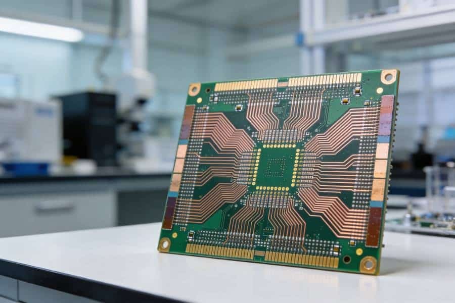
RF & Microwave Laminate Selection Guide
Rogers PCB Material Selection for RF and Microwave Circuits
Rogers PCB materials offer specialized laminate options for circuits that require controlled dielectric behavior, low signal loss and predictable RF performance. Selecting the right material means more than choosing a brand: the laminate grade, dielectric thickness, copper foil, bonding system and finished stackup must work together.
Compare Rogers material families, understand the conditions behind datasheet values, and define the inputs needed for a manufacturable RF or microwave PCB.
- Compare laminate families and material grades
- Review dielectric thickness, copper and bonding materials
- Define RF stackup and quotation requirements
What Is Rogers PCB Material?
Rogers PCB material refers to circuit laminates and related bonding materials manufactured by Rogers Corporation. A Rogers PCB is a printed circuit board fabricated using one or more of these materials in its stackup. The material name identifies the substrate system—not a separate type of electronic circuit or a guarantee of finished-board performance.
These materials are commonly evaluated for RF and microwave designs where dielectric consistency, signal loss, phase behavior, dimensional stability or temperature-related electrical changes are important. The appropriate laminate depends on the circuit architecture, operating environment, manufacturing requirements and electrical performance targets.
A complete specification should identify the exact material grade, dielectric thickness, copper construction and bonding interfaces. Specifying only “Rogers material” leaves important stackup decisions undefined and can lead to quotations based on different constructions.
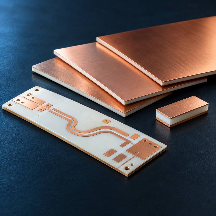
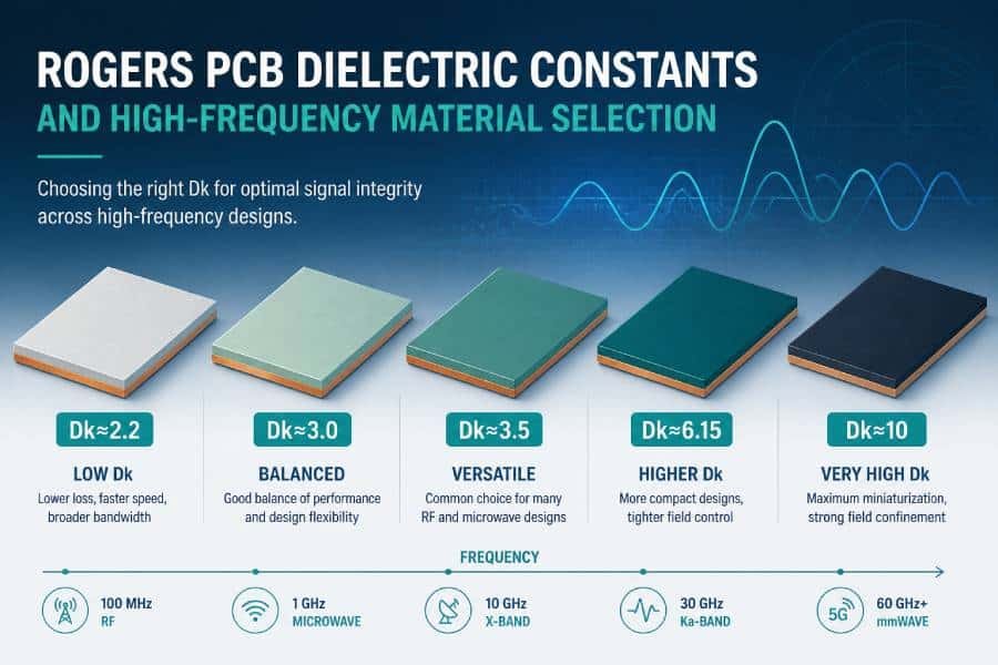
Rogers PCB Material Families: RO4000, RO3000, RT/duroid and TMM
Start with the material family before comparing individual grades. Resin chemistry, fillers and reinforcement affect dielectric behavior, mechanical stability and fabrication requirements. The following overview introduces four commonly evaluated Rogers laminate families.
↔ Swipe or scroll horizontally on smaller screens to compare all columns.
| Material Family | Material Construction | Selection Priorities | What to Review |
|---|---|---|---|
| RO4000 Examples: RO4003C, RO4350B | Hydrocarbon-based thermoset laminates with ceramic fillers and woven-glass reinforcement in common grades. These materials are not PTFE laminates. | Controlled dielectric properties and RF performance combined with fabrication processes broadly compatible with FR-4-style PCB production. | Exact grade, process versus design Dk, dielectric thickness, copper foil, flammability requirements and compatible multilayer bonding materials. |
| RO3000 Examples: RO3003, RO3035, RO3006 | Ceramic-filled PTFE composites. The selected grade determines dielectric constant and other electrical and mechanical characteristics. | Low-loss RF and microwave designs requiring controlled dielectric properties and grade-specific thermal and dimensional behavior. | Required Dk, loss target, dielectric thickness, temperature-related dielectric behavior, bonding system and PTFE-compatible fabrication processes. |
| RT/duroid Examples: RT/duroid 5870, 5880, 6002 | Filled PTFE laminates with reinforcement or filler systems that vary by grade. The 5870 and 5880 grades use glass-microfiber-reinforced PTFE. | Grade-specific microwave performance, including low-Dk options and specialized electrical, thermal or dimensional requirements. | Exact product rather than the family name alone, copper type, handling requirements, laminate thickness and the proposed fabrication route. |
| TMM Examples: TMM 3, TMM 4, TMM 10i | Ceramic-filled thermoset polymer composites. TMM materials are a different resin system from PTFE-based laminates. | Microwave circuits requiring selected dielectric constants, dimensional stability and controlled thermal expansion behavior. | Grade-specific Dk and loss, temperature stability, available thickness, copper compatibility and assembly or interconnection requirements. |
This is a material-family overview, not an exhaustive Rogers product list or a statement of stocked materials. Confirm the exact grade, current supplier datasheet, thickness, copper option and project availability before releasing the stackup.
Compare Common Rogers PCB Material Grades
Use the following comparison to shortlist material candidates, not to approve a finished stackup. Similar dielectric constants do not make different laminates interchangeable. Compare the resin system, measurement conditions, dielectric thickness, copper construction and fabrication requirements together.
↔ Swipe or scroll horizontally on smaller screens to compare all columns.
| Material | Material System | Process Dk | Design Dk Reference | Typical Df at 10 GHz | Selection Focus |
|---|---|---|---|---|---|
| RO4003C | Woven-glass-reinforced hydrocarbon/ceramic thermoset | 3.38 ± 0.05 | 3.55 | 0.0027 | A candidate when RF dielectric control, material loss and FR-4-style fabrication compatibility must be balanced. |
| RO4350B | Woven-glass-reinforced hydrocarbon/ceramic thermoset | 3.48 ± 0.05 | 3.66 | 0.0037 | A widely evaluated RO4000 option for RF stackups. Review the exact electrical, thermal, flammability and multilayer construction requirements. |
| RO3003 | Ceramic-filled PTFE | 3.00 ± 0.04 | 3.16* | 0.0010 | A low-loss PTFE-based candidate when dielectric behavior and temperature stability are important. Confirm fabrication and bonding compatibility. |
| RT/duroid 5870 | Glass-microfiber-reinforced PTFE | 2.33 ± 0.02 | 2.33 | 0.0012 | A low-Dk candidate for microwave transmission-line designs. Review geometry, laminate handling, copper foil and the proposed manufacturing route. |
| RT/duroid 5880 | Glass-microfiber-reinforced PTFE | 2.20 ± 0.02 | 2.20 | 0.0009 | A low-Dk, low-dielectric-loss candidate for demanding microwave designs. Evaluate conductor loss and the complete stackup rather than Df alone. |
- Process Dk and Df values shown here are supplier references associated with 10 GHz characterization. Confirm the exact method, conditioning, direction and specification in the current material datasheet.
- Design Dk values are separate design references. Their measurement methods and frequency ranges are not necessarily identical to those used for Process Dk.
- *The current Rogers RO3003 product-page table lists a Design Dk reference of 3.16. Verify the applicable supplier document and design context; older documents may list different values.
- Df is a material loss parameter, not the insertion loss of a finished transmission line. These values do not constitute PCBELEC finished-board acceptance limits.
- Supplier references: RO4003C, RO4350B, RO3003 and RT/duroid 5870 and 5880.
How to Read Rogers Material Datasheets
A datasheet describes a specific material under defined measurement conditions. Use it to compare candidates and establish design inputs, but do not treat every listed value as a guaranteed property of the finished PCB or as an interchangeable input for every simulation.
Process Dk vs Design Dk
Process Dk is associated with the supplier's material characterization or specification method. Design Dk is a separately provided reference intended to support circuit modeling. The two values can differ because their measurement methods and electromagnetic test configurations differ.
Neither should be confused with the effective dielectric constant of a finished transmission line, which also depends on the circuit geometry and surrounding dielectric structure.
Confirm which Dk reference is appropriate for the design model, laminate thickness and operating frequency.
Dissipation Factor and Measurement Frequency
Dissipation factor, also called Df or loss tangent, describes dielectric loss under the stated test conditions. Compare values at relevant frequencies and with compatible measurement methods rather than comparing isolated numbers.
A lower Df can reduce the dielectric contribution to transmission-line loss. It does not account for all conductor, surface-finish, radiation or transition losses in the finished structure.
Define the circuit's insertion-loss target separately from the material's datasheet Df.
Thermal Coefficient of Dielectric Constant
Thermal coefficient of dielectric constant, or TCDk, describes how Dk changes with temperature over the stated range. It is relevant when temperature-related changes in electrical length, phase or resonant frequency could affect circuit performance.
TCDk is different from thermal expansion. Evaluate dielectric temperature response and physical dimensional change as separate inputs.
Review the temperature range and electrical drift permitted by the application, not only room-temperature Dk.
CTE, Moisture and Dimensional Stability
Coefficient of thermal expansion, or CTE, describes physical expansion with temperature. Check the specified direction: in-plane behavior affects dimensional matching, while Z-axis behavior is relevant to thickness changes and interconnection reliability.
Moisture absorption and dimensional stability should also be reviewed for the intended operating environment and processing conditions. These properties cannot be inferred from Dk or material family alone.
Confirm thermal, humidity and dimensional requirements for the proposed laminate and complete stackup.
Dielectric Thickness, Copper Foil and Bonding Materials
A Rogers material grade does not define a complete PCB stackup. Dielectric thickness, copper construction and bonding layers must be specified together because they affect transmission-line geometry, impedance, loss, mechanical thickness and manufacturing compatibility.
Core and Finished Dielectric Thickness
Specify the dielectric spacing used by the electrical model, not only the finished board thickness. For an RF transmission line, the spacing between the signal conductor and its reference plane is a critical part of the geometry.
Core thickness and laminated bonding-layer thickness are different specifications. Confirm whether a supplier's thickness designation excludes or includes copper and how the finished dielectric spacing will be controlled.
Copper Thickness and Surface Profile
Copper weight alone does not describe the RF conductor. Review foil type, surface profile and the finished copper thickness after any plating. These inputs also influence trace geometry and fabrication requirements.
Smoother copper can reduce conductor loss in suitable high-frequency structures. Standard and LoPro constructions should therefore be treated as defined material configurations, not assumed to be interchangeable.
Bondply and Prepreg Selection
Bonding materials join cores and create additional dielectric regions in multilayer boards. Their electrical properties, flow behavior, cured thickness and lamination requirements must be considered wherever they affect the RF structure.
Rogers offers dedicated bonding-material families, including RO4400/RO4400T products. Select a compatible construction for the actual laminate grades and manufacturing process; do not assume one bonding material suits every Rogers family.
↔ Swipe or scroll horizontally on smaller screens to review all specifications.
| Specification | What It Describes | Why It Matters | What to Confirm |
|---|---|---|---|
| Core Dielectric Thickness | The dielectric thickness of a selected laminate core, distinguished from its copper layers. | Defines part of the signal-to-reference geometry and influences the required trace dimensions. | Exact grade, thickness designation, tolerance and available copper configuration. |
| Copper Foil and Finished Copper | Starting foil construction and the final conductor thickness after the applicable fabrication processes. | Affects conductor loss, trace cross-section, etching and the electrical model. | Foil type, surface profile, starting thickness, plating allowance and final copper target. |
| Laminated Bonding-Layer Thickness | The finished dielectric layer created by the selected prepreg, bondply or bonding-film construction. | Can influence RF fields, impedance, stackup thickness and layer registration. | Material grade, build-up, resin flow, copper distribution and expected cured thickness. |
| Finished PCB Thickness | The overall board thickness defined by the fabrication drawing and agreed measurement basis. | Controls mechanical fit, connector interfaces, mounting requirements and overall stackup constraints. | Nominal value, tolerance, measurement locations and the surfaces included in the specification. |
Available thicknesses and copper options depend on the exact material grade and supply configuration. A material-selection reference is not a stock commitment or a fixed manufacturing limit.
Rogers vs FR-4: When Is a Material Upgrade Justified?
Choose the material against the circuit requirements, not a universal frequency threshold. Operating frequency matters, but so do transmission-line length, loss budget, impedance tolerance, phase sensitivity, temperature exposure and the required consistency between manufactured boards.
Stay With FR-4 When It Meets the Requirements
A specified FR-4 laminate may be appropriate when the electrical targets can be met with its actual dielectric behavior, available stackup and manufacturing tolerances. Avoid adding specialty materials without a defined benefit.
- The intended trace lengths fit the allowable loss budget.
- Impedance and phase requirements can be met.
- The thermal and environmental conditions are acceptable.
- Cost and standard multilayer processing are priorities.
Separate High Tg From Low-Loss Performance
High Tg describes a thermal-transition characteristic. It does not, by itself, establish low dielectric loss, tight Dk control or suitability for a particular RF circuit. Evaluate thermal and electrical requirements separately.
- Review the complete thermal profile, not Tg alone.
- Check Dk and Df at relevant frequencies.
- Confirm dimensional and interconnection requirements.
- Consider a specified low-loss rigid laminate where appropriate.
Evaluate Rogers When Dielectric Behavior Becomes Critical
A Rogers laminate can be justified when the electrical targets require a combination of loss performance, dielectric consistency or temperature-related stability that the proposed conventional laminate cannot provide.
- Longer RF paths make material loss more consequential.
- Phase or resonant behavior needs tighter control.
- Environmental changes must stay within the design margin.
- Repeatability is important across production lots.
All-Rogers vs Rogers/FR-4 Hybrid Stackups
Multilayer RF boards can use Rogers laminates throughout the core structure or combine selected Rogers layers with FR-4 materials. The appropriate construction depends on where the RF signals travel, which dielectric regions they interact with, and how the complete board will be laminated and assembled.
All-Rogers Stackup
This generally describes a construction using Rogers laminate cores throughout the board, with explicitly selected compatible bonding materials. It does not automatically mean every dielectric layer has the same Dk, Df or resin chemistry.
This path may be appropriate when multiple layers have demanding RF requirements or when the design benefits from a more consistently specified high-performance dielectric system.
Rogers/FR-4 Hybrid Stackup
A hybrid construction uses Rogers laminates in selected RF-critical regions and FR-4 in other parts of the stackup. It can help balance RF performance with routing needs and material cost when the electrical structure supports it.
The actual dielectric environment of each RF line must remain clear. Placing a Rogers core somewhere in the board does not ensure that every critical signal sees only Rogers dielectric.
↔ Swipe or scroll horizontally on smaller screens to compare stackup approaches.
| Review Factor | All-Rogers Approach | Rogers/FR-4 Hybrid Approach |
|---|---|---|
| Material Allocation | Rogers laminate cores are used throughout the proposed construction; each bonding layer is separately specified. | Rogers materials are assigned to selected RF regions, with FR-4 used where its performance is acceptable. |
| RF Dielectric Environment | Still requires confirmation of the actual core and bonding materials surrounding each critical RF conductor. | Requires particular attention to whether RF fields interact with FR-4 or a different bonding dielectric. |
| Cost Direction | Uses specialty laminate material more extensively. Total cost also depends on bonding, layer count and processing. | May reduce specialty-material usage, but additional construction complexity can offset part of the saving. |
| Lamination Compatibility | Check the selected Rogers grades, bonding system, press requirements and dimensional behavior. | Check compatibility across Rogers, FR-4 and bonding materials, including cure requirements and resin flow. |
| Mechanical and Thermal Balance | Review copper balance, material symmetry, thickness and thermal-expansion behavior. | Review the same factors while accounting for the different materials and their placement in the stackup. |
| Best-Fit Direction | Designs with demanding RF requirements distributed across multiple layers or a broadly specified specialty-material construction. | Designs with clearly defined RF-critical regions alongside less demanding digital, control or other layers. |
These are construction approaches, not fixed stackup recipes. Final material allocation and bonding interfaces require electrical review and manufacturing confirmation.
Manufacturing Factors That Affect RF Performance
A Rogers laminate provides a defined material foundation, but the finished RF structure also depends on how that material is processed. The proposed fabrication stackup should preserve the electrical assumptions used in the design model and identify which dimensions or processes require additional control.
Dielectric Thickness and Tolerance
Signal-to-reference spacing affects transmission-line geometry. Specify the critical dielectric thicknesses and tolerances separately from the finished board thickness.
Include laminated bonding layers wherever they form part of the electrical structure, and review the expected finished spacing before approving trace dimensions.
Copper Foil, Plating and Surface Profile
Starting foil, copper surface profile and finished copper thickness influence conductor behavior. A copper-weight callout alone does not fully define these inputs.
Confirm the selected foil configuration and any plating that changes the final conductor cross-section. Material or copper substitutions should be reviewed before release.
Etching and Critical Trace Features
Trace width, coplanar gaps and other RF-critical features should have defined manufacturing requirements. The proposed etching and copper construction must support the intended geometry.
Identify features whose dimensions cannot be changed without design approval. Do not assume that routine impedance adjustments are acceptable for every RF structure.
Surface Finish and Solder Mask
Surface finish and protective coatings can affect exposed RF structures. Their influence depends on the transmission-line type, conductor geometry, operating frequency and where the coating is applied.
Define finish coverage and solder-mask openings deliberately. Avoid selecting a finish solely from a generic list of “best finishes for RF.”
Lamination and Hole Processing
Different Rogers material families require compatible bonding and hole-processing methods. PTFE-based and hydrocarbon/ceramic constructions should not be treated as identical fabrication systems.
Review bonding interfaces, layer registration, drilled features and interconnection requirements against the exact grades in the proposed stackup.
Inspection, Impedance and RF Verification
Define the required inspection and electrical verification scope before quotation. Dimensional inspection, continuity testing and impedance measurements answer different questions from RF insertion-loss or phase measurements.
Where RF verification is required, agree the test structure, frequency range, reference planes, reporting format and acceptance criteria before fabrication.
Have Your Material and RF Geometry Defined?
Share your proposed laminate grades, critical dielectric spacing, copper requirements and RF features for a stackup and manufacturability review before prototype release.
How to Specify Rogers PCB Material for Quotation
A useful Rogers PCB quotation starts with more than the material name. Provide the proposed stackup, critical RF requirements and manufacturing inputs so the construction can be reviewed consistently. If a material or thickness is not yet selected, identify it as an engineering-review item rather than leaving the requirement ambiguous.
↔ Swipe or scroll horizontally on smaller screens to view the RFQ checklist.
| RFQ Input | Information to Provide | Why It Matters |
|---|---|---|
| Design Files and Revision | Gerber or agreed manufacturing files, drill files, board outline, fabrication drawing and the applicable design revision. | Establishes the exact design being quoted and reduces inconsistencies between files and written requirements. |
| Material Grades | Exact laminate grades, required product variants, customer-specified materials and any approved alternative-material policy. | Prevents different quotations from using materially different constructions under a generic “Rogers” label. |
| Stackup and Dielectric Spacing | Layer count, core and bonding materials, critical dielectric thicknesses, tolerances, reference planes and all-Rogers or hybrid construction. | Connects the electrical design to a defined, reviewable manufacturing stackup. |
| Copper Construction | Starting copper thickness, required foil configuration or surface profile, finished copper targets and any critical plating restrictions. | Supports conductor modeling, trace fabrication and material-availability review. |
| RF and Impedance Requirements | Operating frequency range, critical RF layers, line types, impedance targets, tolerances and any insertion-loss, phase or return-loss criteria. | Separates general board fabrication requirements from application-specific electrical expectations. |
| Critical Geometry | RF trace widths, coplanar gaps, coupling features, controlled dimensions and any limits on manufacturer-led geometry adjustments. | Identifies features that require design approval before modification. |
| Finish and Mask Coverage | Surface finish, selective finish requirements, solder-mask coverage and exposed RF areas. | Defines conductor surfaces and coatings that can affect the intended electrical structure. |
| Mechanical Requirements | Finished thickness, outline tolerances, holes, slots, cutouts, mounting interfaces and panel requirements. | Confirms mechanical fit, fabrication features and panelization constraints. |
| Quantity and Project Stage | Prototype quantity, production quantity, expected annual demand, delivery target and any staged qualification plan. | Supports material procurement, panel planning and quotation assumptions. |
| Verification and Documentation | Inspection scope, coupons, electrical tests, RF measurement requirements, reporting, traceability and customer acceptance standards. | Allows the required verification scope and deliverables to be agreed before production. |
Not every project requires every item. Clearly separate mandatory specifications, preferred options and inputs that still require engineering review.
Specify How Material Substitutions Are Approved
State whether the specified grade is mandatory or whether alternatives may be proposed for review. Similar nominal Dk values alone do not establish material equivalence.
Changes to laminate grade, dielectric thickness, copper foil or bonding materials may require updated modeling or validation. Define the approval process before procurement and fabrication begin.
Describe the Electrical Use Case
Include a short description of the circuit's RF function, critical signal paths and operating environment. This gives the engineering team context beyond a material grade and layer count.
If RF measurements are required, identify the test structure, frequency range, reference planes, acceptance limits and reporting needs. Test availability and scope should be confirmed for the specific project.
Have Your Rogers PCB Requirements Ready for Quotation?
Bring your material specification, stackup and fabrication files into the next stage. Explore our high-frequency PCB manufacturing services for Rogers-based RF and microwave board projects.
When Rogers PCB Material Is Not the Right Choice
Rogers materials should be selected for a defined electrical, environmental or manufacturing benefit—not simply because a design includes high-frequency signals. If a different material system meets the requirements more effectively, it may provide a more practical path.
When a Specified FR-4 Laminate Is Sufficient
If the proposed FR-4 construction meets the loss budget, impedance tolerance, environmental conditions and required repeatability, a specialty RF laminate may add cost without delivering a necessary system-level improvement. Evaluate the actual laminate and circuit geometry before upgrading.
When the Main Requirement Is Thermal Robustness
If the board remains rigid and the primary concern is assembly exposure or thermal reliability rather than RF dielectric performance, a suitable High Tg FR-4 construction may be a better fit. High Tg does not guarantee low loss, so thermal and electrical requirements must still be evaluated separately.
When Flexibility or Heat Spreading Dominates
A conventional rigid RF laminate does not replace a dedicated flex material system or metal-core thermal structure. If repeated bending, compact flexible interconnection or direct heat spreading is the main constraint, begin with the relevant material architecture and then assess its electrical suitability.
When the Performance Problem Is Outside the Laminate
Changing the laminate may not resolve poor connector launches, reference-plane discontinuities, unsuitable transitions or other structural limitations. Identify the dominant cause of the performance gap before replacing the material or committing to a more complex stackup.
Compare Other PCB Material Paths
Explore the material direction that matches your main design requirement, whether it is rigid-board cost, thermal stability, cross-family RF selection or a customer-specified laminate system.
FR-4 PCB Material
A practical starting point for rigid multilayer, signal and control boards where the specified laminate can meet the electrical and environmental requirements.
Explore FR-4 Material →High Tg PCB Material
A rigid-laminate direction for projects that prioritize thermal robustness while evaluating dielectric performance as a separate requirement.
Explore High Tg Material →RF / High Frequency PCB Materials
A broader selection path for comparing dielectric systems against frequency, loss, impedance and environmental requirements.
Compare RF Materials →Specialty Laminates
A material-review path for customer-approved grades, unusual dielectric targets or application-specific laminate and documentation requirements.
Explore Specialty Materials →Frequently Asked Questions About Rogers PCB Material
Find answers to common questions about Rogers laminate families, dielectric values, material substitutions and stackup requirements. For a project-specific recommendation, review the exact material grade together with the proposed circuit geometry, operating conditions and manufacturing plan.
Rogers PCB material refers to circuit laminates and related bonding materials manufactured by Rogers Corporation. These products include several resin and reinforcement systems rather than one universal substrate. A complete PCB specification should identify the exact grade, dielectric thickness, copper configuration and bonding materials.
No. RO3000 and several RT/duroid materials are PTFE-based, while RO4000 uses hydrocarbon/ceramic thermoset systems and TMM uses ceramic-filled thermoset polymer systems. Reinforcement and fillers also vary by grade, so neither “PTFE” nor “glass-free” should be used as a description of the entire Rogers portfolio.
RO4003C and RO4350B are both woven-glass-reinforced hydrocarbon/ceramic laminates, but they have different dielectric references, loss characteristics and material qualifications. Their commonly listed Process Dk values are 3.38 and 3.48, respectively, with typical Df values of 0.0027 and 0.0037 at 10 GHz. RO4350B is also formulated for UL 94 V-0 requirements. Select between them using the current supplier datasheet and the complete project requirements rather than treating them as interchangeable.
Use the dielectric reference appropriate to the design method, frequency range and transmission-line structure. Process Dk is associated with a supplier characterization or specification method, while Design Dk is a separate modeling reference. Confirm the applicable supplier guidance and distinguish either value from the effective dielectric constant of the finished transmission line.
No. A lower Df can reduce the dielectric contribution to loss, but it does not account for conductor roughness, surface finish, trace geometry, radiation or transition losses. The best material is the one that meets the circuit's electrical, environmental and manufacturing requirements as part of a complete stackup.
Yes. Suitable Rogers/FR-4 hybrid constructions can place specialty materials in RF-critical regions and FR-4 in less demanding parts of the board. The actual dielectric environment around each RF conductor, reference-plane arrangement, bonding interfaces and lamination compatibility must be reviewed before the stackup is approved.
Not automatically. Similar nominal Dk values do not establish equivalent loss, thickness tolerance, copper construction, temperature response or processing behavior. A proposed replacement should be reviewed against the electrical model, manufacturing stackup and any customer material-approval requirements.
Specify the dielectric spacing required by the circuit geometry and electrical model, not only the finished board thickness. Core thickness, laminated bonding-layer thickness and overall PCB thickness are different specifications. Available thicknesses and copper configurations depend on the exact grade and supply option, so confirm the proposed construction before finalizing critical RF features.
No. Impedance verification does not establish the complete circuit's insertion loss, return loss, phase response or operating behavior. Where RF measurements are required, agree the test structure, frequency range, reference planes, acceptance limits and reporting requirements before fabrication.
Provide fabrication files, board dimensions, quantity, layer count, exact material grades, stackup, dielectric thicknesses, copper configuration, surface finish and critical RF geometry. Include impedance requirements, operating frequency, any RF acceptance criteria, mechanical features, documentation needs and the approval policy for material or thickness changes.
Material Review & RF PCB Manufacturing
Turn Your RF Material Requirements Into a Manufacturable Rogers PCB
Share your laminate candidates, proposed stackup, dielectric spacing, copper requirements and fabrication files. Our engineering team can review the construction for material compatibility and manufacturability, with your RF requirements and production targets clearly defined.
- Laminate and bonding-material review
- Critical stackup and DFM review
- Prototype and production fabrication
Material availability, construction options and any specialized RF verification requirements are confirmed during project review.