Heavy Copper PCB Manufacturing &
Thick Copper PCB Fabrication Service
Custom heavy and thick copper PCBs up to 12oz for high-current, high-thermal power electronics, automotive, industrial, and military applications.
JHYPCB is a China-based heavy copper PCB manufacturer specializing in thick and extreme copper circuit boards for demanding power and thermal management designs. We provide engineering-driven fabrication with optimized stackups, reliable plating, and robust solder mask for long-term performance under high current and harsh environments. Prototype and small to medium production runs are all welcome.
- Copper thickness: 3–12oz on outer and inner layers (heavy & extreme copper options).
- 2–32 layer heavy copper PCB stackups with FR4, high Tg, aluminum, and hybrid materials.
- Designed for high-current, high-power density, and improved thermal performance.
- DFM review, rapid prototyping, and reliable production for global customers.
What Is a Heavy / Thick Copper PCB?
A heavy copper PCB, also called a thick copper PCB, is a printed circuit board that uses much thicker copper layers than standard PCBs. While conventional boards typically use 0.5–3 oz/ft² copper, heavy copper PCBs start from about 3–4 oz/ft² and can go up to 20 oz/ft² or even higher for extreme copper designs.
By increasing the copper thickness on the inner and outer layers, heavy copper PCBs can safely carry higher currents, reduce temperature rise, and improve mechanical strength at connectors, vias, and high-stress areas. This makes heavy and extreme copper boards ideal for high‑power, high‑reliability applications such as power supplies, motor drives, automotive and industrial power modules, and other harsh‑environment electronics.
Typical Copper Thickness Ranges
| Type of PCB | Typical Copper Thickness Range (per layer) | Typical Usage Examples |
|---|---|---|
| Standard PCB | 0.5–3 oz/ft² | Consumer electronics, low to medium power |
| Heavy / Thick Copper PCB | 3–20 oz/ft² | Power supplies, motor control, automotive, industrial power |
| Extreme Copper PCB | 20–200 oz/ft² or more | Very high current bus bars, special power distribution, military and industrial systems |


Why Use Heavy / Thick Copper PCBs?
Heavy and thick copper PCBs are designed to handle much higher current and thermal loads than standard circuit boards. They enable more compact, robust, and reliable power electronics by combining high current‑carrying capability, improved heat spreading, and stronger interconnections on a single board.
Heavy Copper PCB Applications & Industries
Heavy and thick copper PCBs are widely used in high‑power, high‑current, and harsh‑environment electronics where standard PCBs cannot provide enough current carrying capacity, thermal performance, or mechanical strength. JHYPCB manufactures heavy copper circuit boards for a broad range of power electronics, automotive, industrial, and military applications.

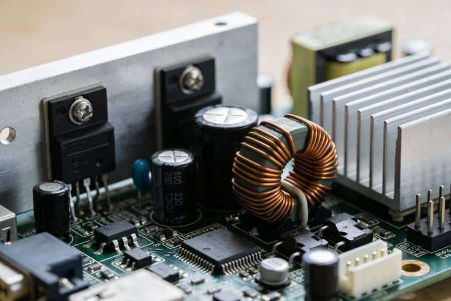
Power Supplies & Power Conversion

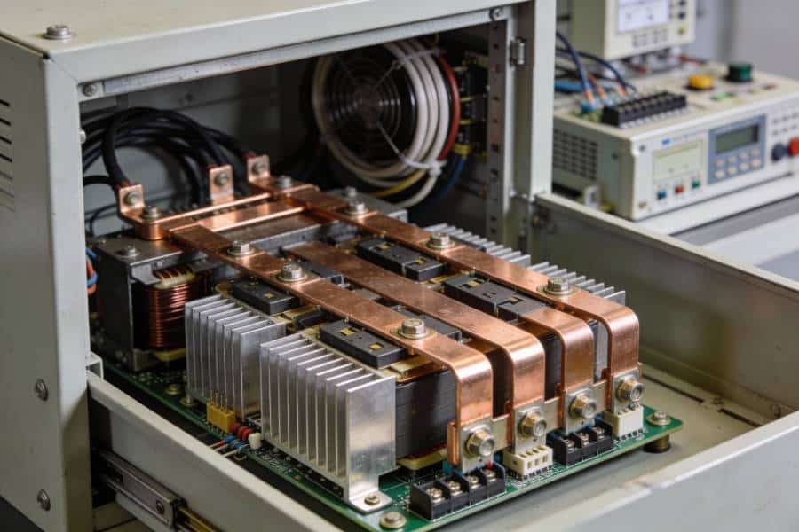
Motor Drives & Industrial Control

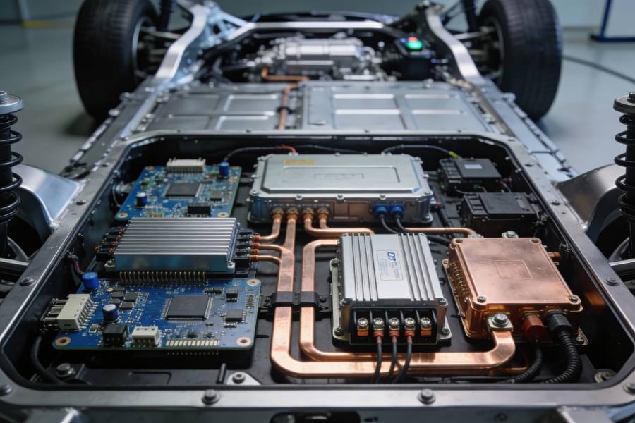
Automotive & Electric Vehicles (EV/HEV)

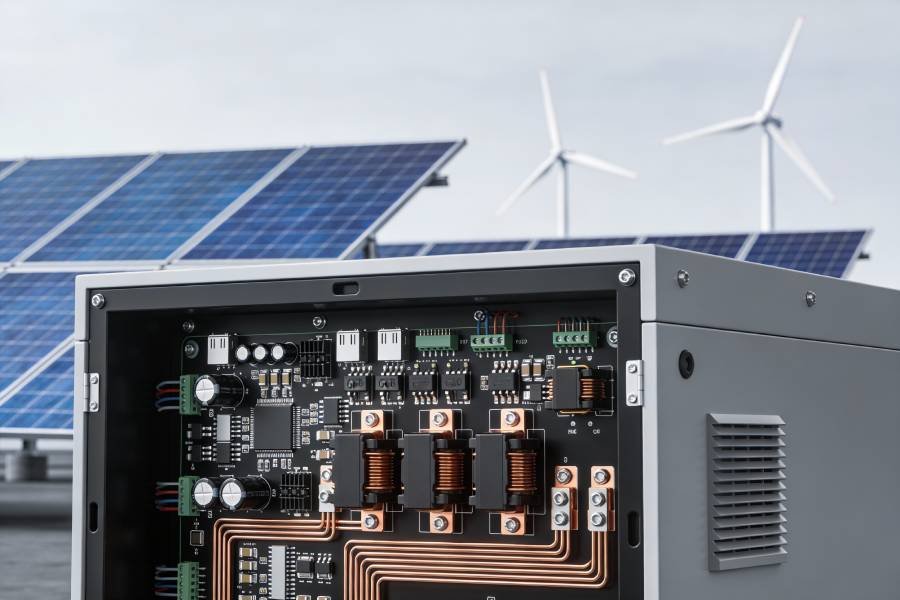
Renewable Energy & Power Storage

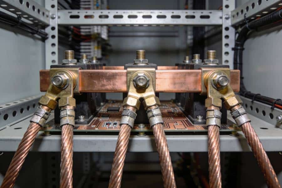
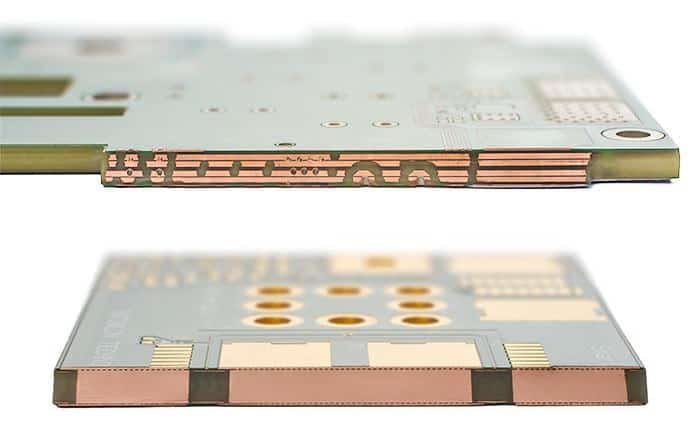
High‑Current Bus Bars & Power Distribution

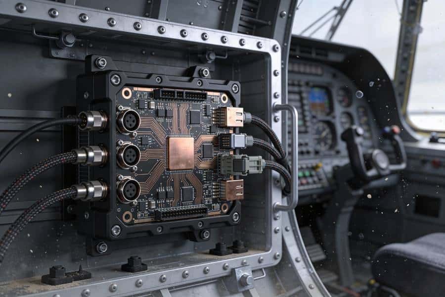
Military, Aerospace & Harsh‑Environment Electronics
JHYPCB Heavy Copper PCB Capabilities
JHYPCB provides comprehensive heavy and thick copper PCB manufacturing capabilities for high‑current and high‑power designs. Our engineering team can help you select the right copper weight, stackup, materials, and design rules to balance current carrying capacity, thermal performance, and manufacturability.
Copper Thickness and Design Rules
| Item | Capability / Typical Range |
|---|---|
| Copper thickness (outer layers) | 3–12 oz/ft² heavy copper (up to 12–13 oz on request) |
| Copper thickness (inner layers) | 3–10 oz/ft² (depending on layer count and stackup) |
| Minimum trace/space @ 3 oz | e.g. 8/8 mil (0.20/0.20 mm) |
| Minimum trace/space @ 6 oz | e.g. 12/12 mil (0.30/0.30 mm) |
| Minimum trace/space @ ≥8 oz | e.g. 16/16 mil (0.40/0.40 mm) or as agreed by DFM |
| Maximum finished board size | e.g. up to 500 × 600 mm (or your real value) |
| Surface finishes | ENIG, ENEPIG, immersion silver, immersion tin, OSP, lead‑free HASL |
Layers, Board Thickness and Materials
| Item | Capability / Typical Range |
|---|---|
| Number of layers | 1–30 layers heavy and thick copper PCB stackups |
| Finished board thickness | e.g. 0.8–6.0 mm (or 0.15–10.0 mm according to your real capability) |
| Base materials | FR4, high Tg FR4, halogen‑free FR4, aluminum‑based, hybrid builds |
| Glass transition temperature | e.g. Tg 130–180 °C depending on material selection |
| Solder mask types | High‑temperature solder mask suitable for heavy copper profiles |
| Thermal management options | Heavy copper planes, copper coins, thermal vias, metal‑core options |
For demanding high‑current or high‑temperature designs, we can support custom heavy copper stackups, mixed copper weights on different layers, and hybrid constructions such as FR4 plus metal‑core or aluminum substrates. Our engineers are available to review your Gerber files and specifications and recommend suitable design rules for trace width, spacing, via structures, and thermal management on heavy copper PCBs.
Design for Manufacturability (DFM) Guidelines for Heavy Copper PCBs
Heavy and thick copper PCBs require different design rules than standard boards because the plating, etching, and solder mask processes must handle much thicker copper. Following a few key DFM guidelines will help ensure reliable fabrication, stable quality, and competitive cost for your heavy copper PCB projects.
Recommended Design Considerations
1) Trace width and spacing for each copper thickness
- Use wider traces and larger spacing as copper weight increases to maintain good etching quality and avoid over‑etching or shorts.
- As a general guideline, minimum trace/space values at 3 oz, 6 oz, and ≥8 oz should be significantly larger than those used on 1 oz or 2 oz designs, and should follow the capabilities confirmed by our engineering team.
- For very high current paths, calculate trace width based on allowable temperature rise and consider using parallel traces or copper planes to spread current.
2) Via structures and plating thickness
- Heavy copper designs often need thicker copper plating in through‑holes and vias to safely carry current between layers.
- Use larger via diameters and adequate annular rings to support higher plating thickness and improve mechanical robustness.
- For very high current interconnections, consider multiple vias in parallel (“via arrays”) or special structures such as filled and capped vias in copper pours.
3) Thermal reliefs and pad design
- On heavy copper planes, use appropriate thermal relief patterns to balance solderability and heat‑sinking.
- Oversized pads and robust land patterns help avoid solder joint cracking under thermal cycling and mechanical stress.
- Avoid very narrow thermal spokes on thick copper planes, as they may not remove enough heat during soldering or may be difficult to etch cleanly.
4) Solder mask clearances and dams
- Thicker copper profiles create higher steps at pads and traces, which can affect solder mask coverage.
- Provide sufficient solder mask clearance around pads and use wider solder mask dams between large pads or high‑current conductors to prevent solder bridging.
- Discuss special requirements such as exposed copper areas for bus bars or direct component mounting with our engineers in advance.
5) Board stackup and material selection
- Plan the stackup to balance copper thickness on inner and outer layers, control warpage, and manage thermal expansion.
- Select materials with suitable Tg, Td, and CTI ratings for high‑temperature, high‑power applications.
- For very high power density designs, consider hybrid stackups combining FR4 with aluminum or other metal‑core substrates.
If you share your target current, allowable temperature rise, and preliminary layout with JHYPCB, our engineering team can recommend practical design rules and a cost‑effective heavy copper PCB stackup before you finalize your Gerber files.
Heavy Copper PCB Prototype & Production Service
JHYPCB supports both prototype and small to medium volume production of heavy and thick copper PCBs, helping you move from initial power design validation to stable series manufacturing with a single manufacturing partner. We focus on reliable processes for thick copper plating, controlled etching, and robust solder mask to ensure consistent performance across multiple builds.
Heavy Copper PCB Prototyping
- Flexible order quantities from a few pieces for engineering validation to small pilot runs.
- Support for quick‑turn prototypes depending on copper thickness, layer count, and complexity.
- Engineering review of your stackup, copper weights, and design rules before fabrication to avoid costly re‑spins.
- Capability to build representative prototypes using the same materials and processes planned for production.
Small and Medium Volume Production
- Stable processes for repeated runs of heavy and thick copper PCB orders in small and medium volumes.
- Process control for copper plating thickness, etching, and solder mask registration to maintain consistent quality.
- 100% electrical test and optional additional inspections according to your quality requirements.
- Flexible shipment options for global customers, including partial shipments for time‑critical projects.
Assembly and Value‑Added Services (If Applicable)
- Optional heavy copper PCB assembly services for power modules, power supplies, and control boards.
- Sourcing and mounting of high‑power components, connectors, and thermal interface materials as requested.
- Functional testing, conformal coating, and other value‑added services can be discussed based on project needs.
Why Choose JHYPCB
for Heavy / Thick Copper PCBs?
Choosing the right manufacturer is critical for heavy and thick copper PCB projects because high copper weights put extra demands on plating, etching, and process control. JHYPCB combines specialized process know‑how, engineering support, and quality management to deliver reliable heavy copper PCBs for global customers.
How to Order Heavy Copper PCBs from JHYPCB
Ordering heavy or thick copper PCBs from JHYPCB is straightforward. Our team will review your design, confirm the manufacturable options, and provide a clear quotation and lead time for your prototype or production run.
Step 1: Share your design files and requirements
Send your Gerber files, PCB stackup, target copper thickness for each layer, and key requirements such as current levels, allowable temperature rise, and application information to sales@pcbjhy.com. You can also include any specific standards, test requirements, or documentation you need us to follow.
Step 2: Engineering review and DFM feedback
Our engineering team will review your files for heavy copper manufacturability, including trace width and spacing, via structures, plating, and thermal management. If necessary, we will suggest design adjustments or alternative options to improve reliability, cost, and process capability.
Step 3: Quotation and lead time confirmation
Based on the confirmed design, JHYPCB will provide a detailed quotation covering unit price, tooling, lead time, and shipping terms for prototype or small/medium volume production. We can also discuss partial shipments or multiple builds if your project requires staged deliveries.
Step 4: Manufacturing, testing, and shipment
After you place the order, we start heavy copper PCB fabrication according to the approved specifications and process controls. All boards receive electrical testing, and additional inspections can be performed on request before we pack and ship the PCBs to your location.
Ready to start your next heavy copper PCB project? Contact JHYPCB today to get a heavy copper PCB quotation or upload your files for a free DFM review.
Heavy Copper PCB FAQs
Heavy copper PCBs typically start from about 3–4 oz/ft² copper per layer and can go up to around 20 oz/ft², depending on the application and manufacturer. Extreme copper PCBs usually refer to designs with copper weights above approximately 20 oz/ft² and up to 200 oz/ft² or more for very high‑current bus bar applications.
You should consider a heavy or thick copper PCB when your design needs to carry high continuous or peak currents, handle significant power dissipation, or operate in harsh thermal and mechanical environments. Typical examples include power supplies, inverters, motor drives, automotive power modules, and industrial or military equipment where standard 1–2 oz copper is not sufficient.
Trace width for high‑current heavy copper designs should be calculated based on copper thickness, allowable temperature rise, and whether the trace is on an inner or outer layer. In practice, designers often use IPC‑based current‑carrying capacity charts or calculators and then add additional margin, and JHYPCB can review your layout and recommend practical design rules for each copper weight.
JHYPCB can manufacture heavy and thick copper PCBs with copper weights up to approximately 12 oz/ft² on outer layers and up to around 10 oz/ft² on inner layers, depending on the stackup and design. We support layer counts from 1 to around 30 layers for heavy copper PCB stackups, and we can discuss special constructions for specific high‑power applications.
Heavy copper PCBs from JHYPCB are typically built on FR4, high Tg FR4, halogen‑free FR4, aluminum‑based, or hybrid material systems. Common surface finishes include ENIG, ENEPIG, immersion silver, immersion tin, OSP, and lead‑free HASL; we can recommend suitable finishes based on your assembly process and reliability requirements.
Yes, JHYPCB supports prototypes as well as small and medium volume production for heavy and thick copper PCBs. We can help you validate your design with representative prototypes and then scale to repeatable production runs with consistent copper thickness, quality, and testing.
Related PCB Manufacturing Services

Aluminum PCB Manufacturing
Aluminum‑based PCBs for LED lighting, power supplies, and thermal‑critical applications where excellent heat dissipation is required.

Flexible PCB Manufacturing
Flexible and rigid‑flex PCBs for densely packed electronics that require vibration resistance, dynamic bending, or 3D packaging.

High Tg & High‑Temperature PCB
High Tg FR4 and high‑temperature PCB solutions for applications that operate at elevated temperatures or experience frequent thermal cycling.

PCB Assembly Services
Turnkey PCB assembly services for power electronics, control boards, and mixed‑technology designs that include heavy copper PCBs.


