
Copper-Base PCB Fabrication
Copper Core PCB Manufacturing
Custom copper-base PCBs for LED lighting and power electronics. PCBELEC manufactures 1–4 circuit layers, direct thermal path structures and copper-base hybrid constructions for your next prototype or production order.
Send your fabrication files to sales@pcbelec.com
- Circuit Construction1–4 Circuit Layers
- Thermal StructuresDirect Thermal Path
- Hybrid OptionsCopper Base + FR-4 / FPC
Copper-Base Structures
Copper-Base PCB Construction and Thermal Paths
A copper core PCB, also called a copper-base or copper-based PCB, uses a copper substrate beneath the circuit structure to spread heat from heat-generating components.
PCBELEC manufactures insulated copper-base boards and direct thermal path structures. Explore our copper core PCB materials alongside the construction options below.
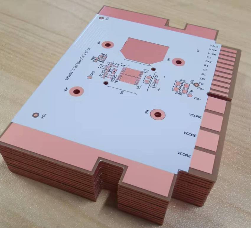
Custom Copper-Base Fabrication
A Copper Thermal Base. A Circuit Structure Built Around Your Design.
Combine a copper substrate with the circuit layers, thermal features and mechanical geometry your board needs. Our fabrication options include insulated circuits, copper thermal pedestals and copper-base structures integrated with FR-4 or FPC.
- 1–4 Circuit Layers
- Thermal Pedestals
- FR-4 / FPC Hybrids
Conventional Copper-Base PCB
A thermally conductive dielectric separates the circuit copper from the copper base. Heat passes through the dielectric into the metal substrate, while the circuit remains electrically insulated from the base.
Simplified Layer Structure
Circuit layer → dielectric → copper base
- Electrically insulated circuit-to-base construction
- Dielectric thermal conductivity of 1–3 W/m·K
- Copper-base thicknesses from 0.5 to 3.0 mm
Copper Thermal Pedestal PCB
A copper pedestal provides a direct metal path from a designated thermal pad to the copper base. The surrounding circuit regions retain their insulating dielectric, separating the electrical routing from the local thermal path.
Simplified Thermal Structure
pedestal
Thermal pad → copper pedestal → copper base
- Direct metal heat path beneath the thermal pad
- Copper thermal pedestal thickness up to 6.0 mm
- Custom thermal-pad and pedestal geometries
Additional processes include 2–4 circuit layers on one side of the copper base, insulated component holes and copper-base hybrid lamination.
Explore Manufacturing Capabilities →Fabrication Specifications
Copper Core PCB Manufacturing Capabilities
From single-layer copper-base boards to multilayer and hybrid structures, PCBELEC combines defined circuit geometry, copper thermal features and precision mechanical processing.
Swipe horizontally to view all manufacturing specifications.
| Specification | Manufacturing Capability |
|---|---|
| Circuit Layers | 1–4 circuit layers |
| Copper Base Thickness | 0.5–3.0 mm |
| Finished Board Thickness | 0.2–6.0 mm |
| Maximum Manufacturing Panel Size | 600 × 2000 mm |
| Dielectric Thermal Conductivity | 1–3 W/m·K |
| Circuit Copper Thickness | Standard: ≥25 μm; special heavy-copper builds: up to 350 μm (10 oz) |
| Minimum Trace Width / Spacing | 5 / 5 mil |
| Minimum PTH Diameter | 0.35 mm |
| Minimum NPTH Diameter | 0.5 mm |
| Copper Thermal Pedestal Thickness | Up to 6.0 mm |
| Single-Side Multilayer Construction | 2–4 circuit layers on one side of the copper base |
| Hybrid Construction | Copper base combined with FR-4 or FPC |
| Surface Finish Options | OSP, HASL, ENIG, immersion silver and immersion tin |
| Warpage | ≤0.5% |
Specialized Copper-Base Processes
-
01
Direct Thermal Path
Copper pedestal structures connect designated thermal pads directly to the copper base, with thermal pedestal thicknesses up to 6.0 mm.
-
02
Insulated Component Holes
Insulated hole construction supports through-hole component connections in copper-base boards.
-
03
Single-Side Multilayer Circuits
Build 2–4 circuit layers on one side of the copper base for more complex routing and interconnection layouts.
-
04
Copper-Base Hybrid Builds
Combine copper-base structures with FR-4 or FPC through hybrid lamination for integrated rigid or flexible circuit regions.
Detailed Process Specifications and Tolerances
Review copper plating, hole positioning, solder mask, legend and mechanical processing specifications.
Swipe horizontally to view all process details.
| Process Item | Specification |
|---|---|
| Copper Thickness Tolerance | ±5 μm |
| Hole Position Tolerance | ±0.075 mm (3 mil) |
| Minimum Via Annular Ring | 5 mil |
| Copper Plating in Insulated Holes | ≥22 μm |
| Solder Mask Thickness | 15–25 μm |
| Minimum Solder Mask Dam Width | 5 mil (0.127 mm) |
| Minimum Legend Line Width | 0.17 mm |
| Minimum Legend-to-Pad Clearance | 0.10 mm |
| Minimum V-Scoring Workpiece Size | 5 × 5 mm |
| Maximum V-Scoring Panel Size | 585 × 2000 mm |
| V-Scoring Board Thickness | 0.6–3.0 mm |
| V-Scoring Cutter Angle | 30° and 45° |
| V-Scored Outline Tolerance | 0.10 mm |
| Routed Outline Tolerance | ±0.10 mm |
Ready to Quote Your Copper-Base PCB?
Share your Gerber files, drill data, fabrication drawing and order quantity for a custom manufacturing quotation.
Compare PCB Constructions
Copper Core vs. Aluminum Core vs. Heavy Copper PCB
Compare the metal base and the circuit copper separately. Copper-core and aluminum-core PCBs are defined by their metal substrate, while heavy-copper PCBs are defined by thicker copper in the circuit layers.
Swipe horizontally to compare all three PCB constructions.
| Comparison Point | Copper Core PCB Copper-base construction | Aluminum Core PCB Aluminum-base construction | Heavy Copper PCB Thick circuit-copper construction |
|---|---|---|---|
| Defining Feature | A copper substrate beneath the circuit structure. | An aluminum substrate beneath the circuit structure. | Increased copper thickness in the conductive circuit layers. |
| Primary Design Focus | Heat spreading through the copper base and engineered thermal paths. | Metal-base heat spreading with a lightweight substrate. | Current-carrying capacity and thermal management within the circuit copper. |
| Heat-Transfer Structure | Conductive heat transfer through an insulating dielectric, or a direct thermal path beneath designated thermal pads. | Conductive heat transfer through the dielectric into the aluminum base. | Thicker traces and copper areas distribute heat within the circuit structure. |
| Metal Base and Circuit Copper | Copper-base thickness and circuit-copper thickness are separate specifications. | Aluminum-base thickness and circuit-copper thickness are separate specifications. | Heavy circuit copper does not, by itself, specify a copper or aluminum base. |
| Typical Project Requirements | High-power LED boards, concentrated thermal pads and custom copper thermal structures. | LED lighting boards and metal-base designs with weight and cost priorities. | High-current power distribution, power conversion and robust conductive paths. |
| Key Details to Specify | Copper-base thickness, dielectric, circuit copper, thermal-pad geometry and pedestal features. | Aluminum-base thickness, dielectric, circuit copper, board dimensions and mounting features. | Finished circuit-copper thickness, trace geometry, layer structure and plated-hole requirements. |
Specify the substrate, circuit copper and thermal features together when preparing your fabrication package.
Applications & Product Examples
Copper Core PCBs for LED and Power Applications
Explore copper-base PCB examples for automotive, stage and photography lighting, alongside new energy vehicle electronics. PCBELEC combines custom circuit construction, thermal features and board geometry in one fabrication service.
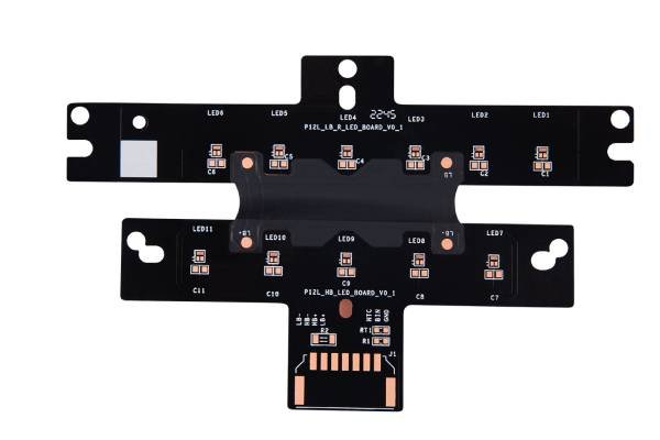
Automotive Lighting
Custom copper-base boards for automotive LED modules, with circuit patterns, thermal interfaces and mounting features built around the lighting assembly.
Available Fabrication Features
- Insulated circuits and direct thermal paths
- Custom outlines and mounting-hole patterns
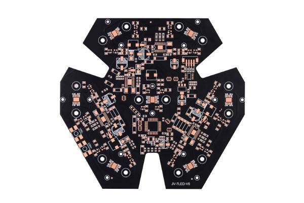
Stage & High-Intensity Lighting
Copper-base PCBs for concentrated LED light sources in stage fixtures, combining the specified light-source arrangement with custom thermal and mechanical features.
Available Fabrication Features
- Copper thermal pedestal structures
- Circular and irregular board profiles
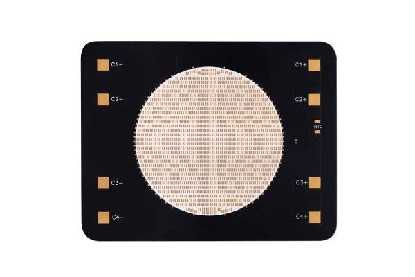
Photography & Studio Lighting
Copper-core boards for photography and studio LED modules, with circuit routing and copper-base construction tailored to the specified light-source layout.
Available Fabrication Features
- Custom LED-array and thermal-pad patterns
- Defined copper and dielectric thicknesses
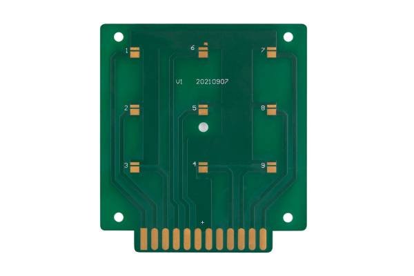
New Energy Vehicle Electronics
Copper-base boards for new energy vehicle electronics, bringing together the circuit, thermal and mechanical requirements of the specified module.
Available Fabrication Features
- Heavy circuit copper and multilayer options
- Insulated holes and hybrid constructions
Preparing the fabrication package for your next board?
Review Manufacturing File Requirements →Inspection & Manufacturing Records
Copper Core PCB Quality Control and Inspection
PCBELEC combines circuit inspection, electrical testing and dimensional verification to check the features that define your copper-base board—from conductive paths and insulated holes to the finished outline and thermal structure.
-
01
Circuit & Electrical Verification
Electrical testing checks circuit continuity and isolation, while optical inspection examines the manufactured circuitry and visible board features.
- Continuity and isolation testing
- AOI inspection of circuit patterns
- Surface finish, solder mask and legend checks
-
02
Dimensions & Mechanical Features
Dimensional inspection checks the finished board against its drawing, including the outline, thickness, mounting features and designated thermal geometry.
- Board thickness and outline measurements
- Hole sizes and position verification
- Pedestal dimensions and board flatness checks
-
03
Cross-Section & Structural Inspection
Microsection inspection examines internal features such as copper plating, hole-wall structure and layer interfaces, providing a closer view of the manufactured construction.
- Copper and plated-hole cross-sections
- Dielectric and layer-interface examination
- Microsection measurements and reporting
Explore our inspection resources or send the fabrication package for your next copper-base PCB order.
Custom Fabrication & Quotation
Request a Custom Copper Core PCB Quote
Get a quotation for your copper-base PCB prototype or production order. Send your fabrication files, board specifications and quantity to PCBELEC.
What Shapes Your Manufacturing Quote
-
01
Board dimensions, order quantity and individual-board or panel delivery.
-
02
Circuit layers, circuit-copper thickness and copper-base thickness.
-
03
Dielectric materials, direct thermal paths, copper pedestals and hybrid construction.
-
04
Hole structures, precision machining, surface finish and solder mask.
-
05
Inspection records, packaging and delivery requirements.
Include These Details with Your Inquiry
Manufacturing File Requirements →Files & Board Revision
Gerber files, drill data, fabrication drawings and the required board revision.
Construction & Materials
Circuit layers, copper-base thickness, circuit copper, dielectric and finished board thickness.
Thermal & Special Features
Thermal-pad and pedestal drawings, insulated holes and FR-4 or FPC hybrid regions.
Finish & Mechanical Details
Surface finish, solder mask, outline tolerances, mounting features and V-scoring details.
Inspection & Documentation
Acceptance criteria, critical measurements, report requirements and identification details.
Quantity & Delivery
Order quantity, board or panel format, packaging, destination and target ship or arrival date.
Copper-Base PCB FAQ
Copper Core PCB Manufacturing FAQ
Answers to common questions about copper-base construction, thermal paths, manufacturing options and quotation requirements.
Discuss your next copper-base PCB build:
sales@pcbelec.comWhat is a copper core PCB?
A copper core PCB uses a copper substrate beneath its circuit structure to spread heat from heat-generating components. It is also called a copper-base, copper-based or copper substrate PCB.
PCBELEC manufactures both insulated copper-base boards and copper thermal pedestal structures. Explore our copper-base constructions and thermal paths .
What is the difference between copper core and heavy copper PCBs?
Copper core describes the board’s metal substrate. Heavy copper describes increased copper thickness in the conductive circuit layers. They refer to different parts of the construction and can be combined in the same board.
Our copper-base fabrication includes heavy circuit copper up to 350 μm. See the copper core, aluminum core and heavy copper comparison for a side-by-side explanation.
What is a direct thermal path copper PCB?
A direct thermal path copper PCB connects a designated component thermal pad to the copper base through a copper pedestal. This creates a direct metal heat path beneath that pad, while surrounding circuit regions retain their insulating dielectric.
PCBELEC manufactures custom copper pedestal structures for LED lighting and power applications.
What copper-base PCB constructions do you manufacture?
We manufacture copper-base PCBs with 1–4 circuit layers, including conventional insulated structures, direct thermal path boards and 2–4 circuit layers on one side of the copper base.
Our specialized processes also include insulated component holes and copper-base constructions combined with FR-4 or FPC. View the full manufacturing capabilities .
What affects the cost of a copper core PCB?
The manufacturing price reflects board dimensions, quantity, circuit layers, copper-base thickness, circuit copper and dielectric construction. Thermal pedestals, hybrid regions, special holes, machining and surface finish also shape the quote.
Send your fabrication files and quantity to request a custom copper core PCB quotation .
Which files should I send for a copper core PCB quote?
Send Gerber files, drill data and a fabrication drawing with the board revision, dimensions, circuit layers, copper thicknesses, dielectric requirements, surface finish and quantity.
Include drawings for thermal pedestals, insulated holes and hybrid regions, together with your delivery and reporting requirements. Review our manufacturing file requirements before submitting the package.