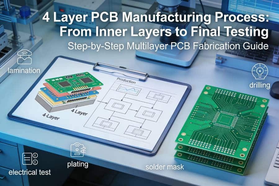
4 Layer PCB Manufacturing Process: Step‑by‑Step Guide from Inner Layers to Final Testing
This guide walks you through the full 4 layer PCB manufacturing process step by step—from FR4 material preparation and inner layer etching to lamination, drilling, plating, solder mask, and final electrical testing—so you can understand how design decisions and DFM rules affect cost, lead time, and reliability.
4 Layer PCB Manufacturing Process: Step‑by‑Step Guide from Inner Layers to Final Testing Read More »