Table of Contents
Introduction: Why Understanding LED PCB Manufacturing Process Matters
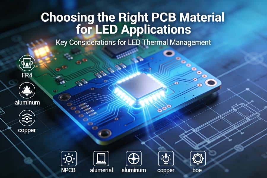
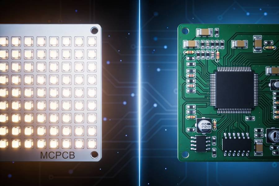
LED PCBs form the backbone of modern lighting systems, displays, and electronics, where efficient heat dissipation, electrical reliability, and precise assembly directly determine product performance and lifespan. Unlike standard FR-4 PCBs, aluminum LED PCBs and metal core PCBs (MCPCB) involve specialized materials and processes to handle high-power LEDs while preventing thermal failures and color inconsistencies.
The LED PCB manufacturing process spans from initial design files to final assembly and testing, with each step requiring tight process control to meet demanding standards for luminous efficiency, safety, and durability. Understanding this workflow helps engineers optimize designs, procurement teams evaluate suppliers, and manufacturers deliver consistent quality.
This comprehensive guide walks through the complete LED PCB manufacturing process—from Gerber file preparation and DFM review, through lamination, plating, and surface finishing, to SMT assembly, testing, and packaging. Whether you need aluminum LED PCB production for street lights, high-power LED PCB assembly for industrial applications, or rapid prototyping, knowing these steps ensures better collaboration with your LED PCB manufacturer and higher success rates for your projects.
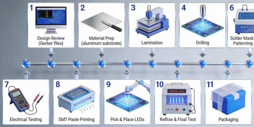
Design File Preparation and Engineering Review
Before any physical production begins, the LED PCB manufacturing process starts with preparing and reviewing design files to ensure manufacturability and catch potential issues early. This critical step prevents costly rework during fabrication or assembly and sets the foundation for high-quality aluminum LED PCB and metal core PCB production.
1 Design File Formats and Standardization
- Engineers submit Gerber files (RS-274X or RS-274D), drill files (Excellon format), BOM, pick-and-place coordinates, and assembly drawings in standard formats compatible with the LED PCB manufacturer’s CAM software.
- For aluminum LED PCB designs, include stack-up drawings specifying metal core thickness, dielectric layer specs, copper weight, and thermal via details.
- The factory standardizes layers (copper top/bottom, solder mask, silkscreen, outline) and verifies layer polarity to avoid mirrored or flipped production errors.
2 DFM (Design for Manufacturability) Analysis
- The engineering team performs DFM review focusing on minimum trace width/spacing (critical for high-density LED layouts), annular ring around pads, thermal via placement under high-power LEDs, and panelization rules.
- For metal core PCBs, they check copper pour areas for heat spreading, avoiding sharp corners that cause etching undercuts, and ensuring adequate clearance between LED pads and mounting holes.
- Special attention goes to surface finish compatibility with LED soldering (ENIG preferred for fine-pitch SMD LEDs) and white solder mask reflectivity for improved light output.
3 Engineering Questions and Design Optimization
- The LED PCB manufacturer asks clarifying questions about LED package types (SMD 2835/5050, COB, high-power through-hole), operating current/voltage, and thermal requirements to suggest optimizations.
- They may recommend adjustments like increasing copper thickness for high-current paths, adding fiducials for precise SMT placement, or optimizing V-scoring for easy depaneling after LED PCB assembly.
- For multi-layer aluminum LED PCBs, engineers verify interlayer alignment tolerances and signal integrity for any control circuits driving the LEDs.
4 Sample Confirmation and Tooling Setup
- After DFM approval, the factory generates engineering panels or first-article samples for customer sign-off, including impedance test coupons if controlled impedance traces are present.
- Tooling setup includes programming drill paths optimized for aluminum substrates, creating custom solder stencils for LED paste printing, and preparing test fixtures for 100% electrical testing.
- Final panel arrays are designed with process rails, tooling holes, and UL marking areas to meet traceability and certification requirements for LED applications.
This preparation phase typically takes 1-2 days for standard designs but ensures downstream processes like lamination, plating, and LED PCB assembly run smoothly with high first-pass yields.
Material Preparation and Inner Layer Processing (Multi-layer)
With design files approved, the LED PCB manufacturing process moves to material preparation and inner layer circuit formation. This phase is crucial for aluminum LED PCBs and metal core PCBs, where material selection directly impacts thermal performance, reliability, and LED lifespan under high-power operation.
1 Base Material Selection for LED PCBs
- Aluminum substrates or MCPCB cores (typically 1.0mm-1.6mm thick) with high thermal conductivity dielectric (1-3 W/m·K) are cut to panel size, inspected for flatness and surface defects.
- FR-4 prepregs for hybrid multi-layer LED PCBs are selected based on Tg (glass transition temperature >170°C), CTE matching with aluminum core, and UL flammability rating (94V-0).
- Copper foil (1oz, 2oz, or thicker for high-current LED traces) is weighed and cleaned to ensure strong adhesion during lamination.
2 Inner Layer Circuit Pattern Transfer
- Photoresist is applied to copper foil surfaces via roller coating or lamination, then exposed using high-precision artwork films or LDI (laser direct imaging) for fine LED control traces.
- Development removes unexposed resist, revealing the inner layer circuit pattern for etching.
- Spray etching removes unwanted copper using ferric chloride or cupric chloride, controlled to maintain trace integrity and avoid undercutting near thermal vias.
3 Inner Layer Etching and AOI Inspection
- Post-etching, tin or tin-lead stripping reveals clean copper traces, followed by resist removal and black oxide or brown oxide treatment for better lamination adhesion.
- Automated Optical Inspection (AOI) scans 100% of inner layers for shorts, opens, mouse bites, and dimensional accuracy critical for multi-layer alignment in LED PCBs.
- For high-power designs, engineers verify copper weight retention and trace resistance to ensure current-carrying capacity for LED arrays.
4 Via Filling and Thermal Management Preparation
- Controlled-depth drilling or laser ablation creates blind/buried vias for interlayer connections, followed by plasma desmear to remove epoxy residue.
- High-power LED PCBs receive conductive or non-conductive via filling (resin plug or copper fill) to prevent thermal shorts through metal cores while maintaining heat paths.
- Black hole (via tenting) or electroless copper plating seeds vias for subsequent PTH plating, ensuring reliable electrical connections without compromising thermal dissipation.
This inner layer processing establishes the foundation for multi-layer aluminum LED PCBs, where precise material matching and defect-free circuits prevent delamination or shorts during thermal cycling in LED applications. Yield targets exceed 98% before advancing to lamination.
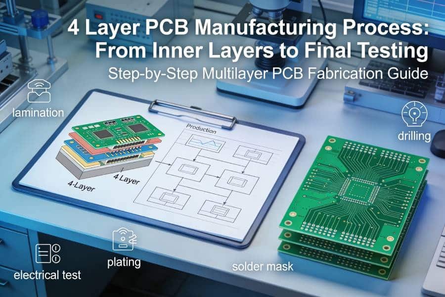
PCB Lamination and Drilling
After inner layers are processed and inspected, the LED PCB manufacturing process advances to lamination, where multiple layers are bonded under heat and pressure, followed by precise drilling. This step is particularly challenging for aluminum LED PCBs and hybrid multi-layer designs, requiring careful control to maintain flatness and thermal integrity.
1 Multi-Layer Lamination Process
- Inner layers, prepregs, and aluminum or copper cores are aligned using tooling pins, then stacked in a press book with separator plates for controlled temperature (180-220°C) and pressure (300-500 psi).
- For aluminum LED PCBs, hybrid lamination bonds FR-4 prepregs to metal cores using thermally conductive adhesives, preventing voids that could create thermal hotspots under high-power LEDs.
- Prepreg flow and cure cycles are optimized to achieve uniform dielectric thickness while matching CTE between aluminum and copper layers, avoiding warpage during LED operation.
2 Lamination Inspection and Debonding
- Post-lamination panels undergo ultrasonic scanning and cross-section analysis to verify bond line thickness, void-free lamination, and no delamination between metal core and circuit layers.
- Sequential lamination for complex aluminum LED PCBs allows building multi-layer structures incrementally, with intermediate inspections to catch alignment or adhesion issues early.
- Pin debonding removes copper flash from PTH edges, ensuring clean surfaces for subsequent plating and preventing defects during LED PCB assembly.
3 Drilling Operations
- Mechanical carbide drills (0.1-6.0mm) or laser drilling create through-holes, vias, and tooling holes, with peck drilling cycles to manage heat and chip evacuation in aluminum substrates.
- For metal core PCBs, controlled-depth drilling stops precisely at the dielectric layer above the aluminum base, avoiding damage to the thermal interface while maintaining electrical connectivity.
- Drill bit breakage prevention uses optimized feed rates and chip load calculations specific to aluminum LED PCB materials, achieving hole position accuracy within ±0.075mm.
4 Desmear, Etch-Back and Activation
- Plasma or chemical desmear removes epoxy smear from hole walls, ensuring uniform electroless copper deposition for reliable plating.
- Permanganate etch-back enlarges hole entrances slightly for better plating coverage while preserving aspect ratios suitable for LED control traces.
- Micro-etch and activator baths prepare hole surfaces for catalytic copper seeding, critical for high-reliability PTH connections in power LED applications.
Proper lamination and drilling lay the groundwork for robust interlayer connections and thermal pathways in aluminum LED PCBs, directly affecting LED junction temperatures and long-term reliability. Process capability indices (Cpk >1.33) ensure these steps meet stringent tolerances before outer layer patterning begins.
Solder Mask, Silkscreen and Surface Finish
With outer layer circuits complete and plated, the LED PCB manufacturing process focuses on protective coatings, markings, and final surface preparation. These steps enhance durability, solderability, and light efficiency for aluminum LED PCBs while preparing boards for reliable LED PCB assembly.
1 Solder Mask Application
- Liquid photoimageable solder mask (LPSM) or dry film is applied to both sides, typically white for high reflectivity under LEDs to boost luminous efficiency by 5-10%.
- Exposure through phototools defines solder mask openings over LED pads, vias, and test points, followed by development to reveal precise pad geometry.
- Thermal curing (150-180°C) hardens the mask, with final thickness controlled at 15-25µm to prevent bridging during reflow while protecting traces from environmental exposure.
2 Silkscreen Printing and Component Legend
- Epoxy-based ink is screen-printed for LED polarity markings, component designators, manufacturer logos, date codes, and UL markings essential for traceability.
- Curing at 120-150°C ensures adhesion and solvent resistance, with legibility verified under magnification for fine-pitch SMD LED identification during assembly.
- For high-volume LED PCB assembly, fiducial marks and alignment targets are added to enable precise pick-and-place machine vision recognition.
3 Surface Finish Selection and Application
- ENIG (Electroless Nickel Immersion Gold, 0.05-0.1µm Au over 3-6µm Ni) is preferred for aluminum LED PCBs due to excellent solderability, coplanarity, and shelf life exceeding 12 months for LED soldering.
- Lead-free HASL provides cost-effective alternative for larger pads but requires careful control to avoid uneven deposits affecting fine-pitch SMD LEDs.
- Immersion silver or OSP (Organic Solderability Preservative) options balance cost and performance, with final thickness testing ensuring compliance with IPC-4552/4553 standards.
4 Final Inspection Before Electrical Testing
- Automated optical inspection (AOI) verifies solder mask registration, silkscreen legibility, surface finish coverage, and dimensional accuracy of all exposed copper features.
- Cross-section analysis samples confirm coating thicknesses, adhesion integrity, and no contamination between layers critical for long-term LED reliability.
- Panels passing visual and dimensional checks advance to electrical testing, ensuring only qualified aluminum LED PCBs proceed to assembly preparation.
These finishing processes create robust, assembly-ready LED PCBs with optimized optical performance and solder joint reliability, directly influencing first-pass yield during high-volume LED PCB assembly downstream.
Electrical Testing and Visual Inspection
After surface finishing, LED PCBs undergo rigorous electrical and visual inspections to verify functionality and quality before advancing to assembly. These tests catch defects early, ensuring high first-pass yields for aluminum LED PCBs and minimizing field failures in demanding LED applications.
1 Electrical Testing Methods
Flying probe testers perform 100% open/short continuity checks on unpanelized boards, ideal for prototype and low-volume aluminum LED PCB runs with complex netlists.
Universal grid or flying grid fixtures enable high-speed testing for production panels, verifying thousands of nets per minute including power/ground planes critical for LED arrays.
High-voltage dielectric withstand testing (up to 500V) confirms insulation integrity between traces and metal cores, preventing arcing under high-power LED operation.
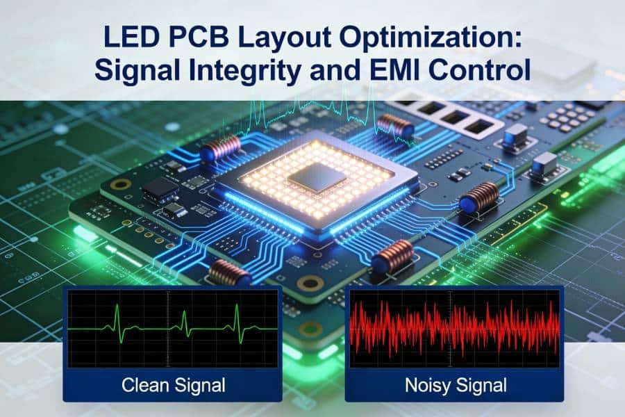
2 Impedance and Thermal Testing
Controlled impedance coupons measure trace characteristic impedance (typically 50-100Ω) for LED driver signal lines, ensuring signal integrity in multi-layer designs.
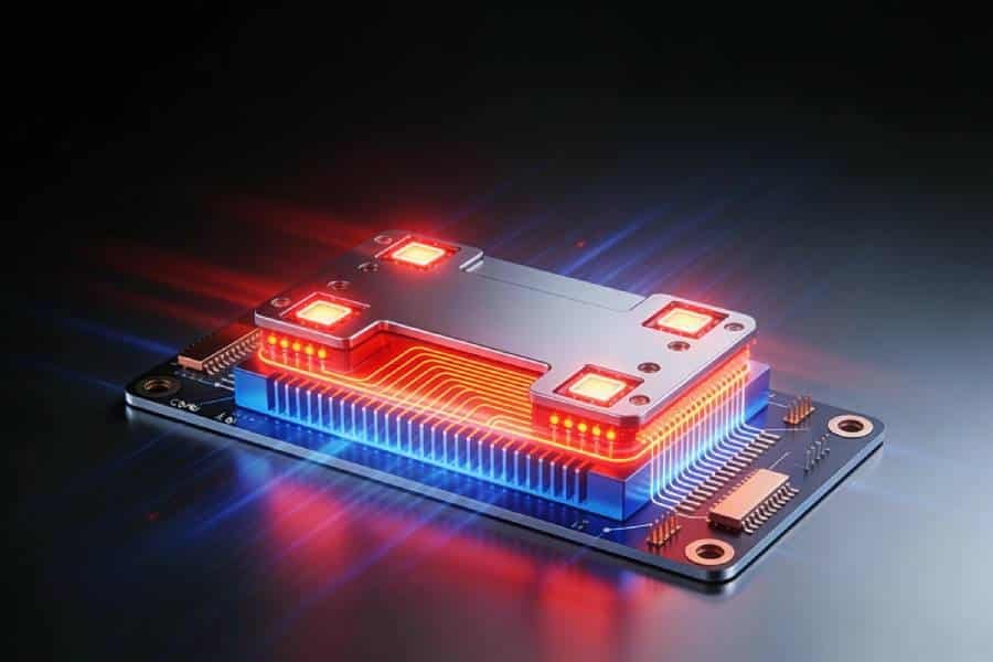
Thermal resistance testing on sample coupons validates heat dissipation paths from LED pads through thermal vias to aluminum cores, targeting <5°C/W for high-power applications.
Leakage current tests between layers and core detect contamination or plating voids that could cause failures during LED PCB assembly reflow or field operation.
3 Visual and Dimensional Inspection
Automated Optical Inspection (AOI) scans 100% of surfaces for solder mask defects, silkscreen issues, surface finish anomalies, and foreign object debris (FOD) that could interfere with LED placement.
3D measurement systems verify critical dimensions including pad sizes, hole positions, board thickness, and flatness (critical for aluminum LED PCBs prone to warpage).
X-ray inspection reveals hidden defects like via fill voids, plating barrel cracks, or delamination invisible to optical methods.
4 Final Yield Analysis and Rework
Statistical process control (SPC) tracks test yields across panels, flagging process drifts affecting trace resistance, hole integrity, or insulation resistance.
Minor defects receive automated optical rework (laser trimming), while panels failing critical electrical parameters undergo scrap analysis to prevent recurrence.
Only panels achieving >99% test pass rates proceed to routing and depanelization, ensuring assembly-ready quality for subsequent LED PCB assembly processes.
Comprehensive electrical testing and inspection create a quality gate that protects downstream LED PCB assembly investment, delivering boards with proven electrical integrity, thermal performance, and cosmetic quality essential for reliable high-volume production.
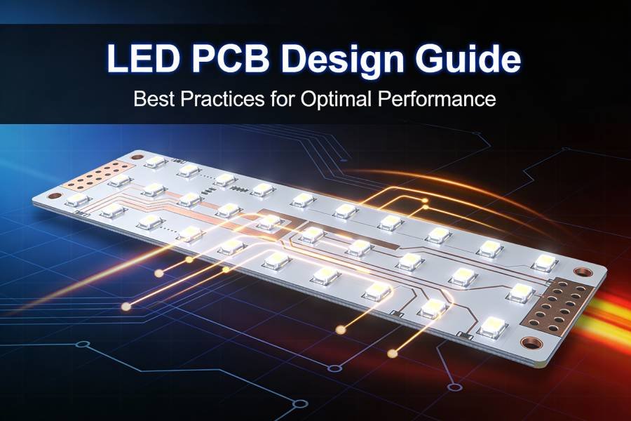
LED PCB Assembly (SMT Process)
With bare LED PCBs tested and approved, the manufacturing process shifts to surface-mount technology (SMT) assembly, where components are precisely placed and soldered. This phase transforms functional aluminum LED PCBs into working lighting modules, requiring tight process control to achieve high yields and consistent performance.
1 Solder Paste Printing
- Laser-cut stainless steel stencils (0.1-0.15mm thick) are aligned to fiducials, then high-precision printers deposit Type-3 or Type-4 solder paste on LED pads using controlled squeegee pressure and speed.
- SPI (Solder Paste Inspection) with 3D laser scanning verifies paste volume, height (75-150µm), and alignment within ±25µm, preventing insufficient wetting or bridging during reflow.
- For high-power LEDs, larger paste deposits ensure robust thermal joints, while fine-pitch SMD LEDs (2835/5050) require precise volume control to avoid tombstoning.
2 Component Placement (Pick-and-Place)
- High-speed chip shooters handle small SMD components (resistors, capacitors) at 50,000-100,000 CPH, feeding from tape, tray, or tube packaging with automated changeover.
- Precision placers mount LEDs, ICs, and connectors using vision systems for ±20µm accuracy, critical for LED binning, polarity, and optical alignment in display modules.
- Flexible mounters handle mixed package sizes from 01005 passives to large COB LEDs, optimizing feeder setup for high-mix LED PCB assembly runs.
3 Reflow Soldering
- Multi-zone nitrogen reflow ovens follow optimized profiles (peak 245-260°C, 60-90s above liquidus) tailored to SAC305 or low-temp alloys, preventing LED phosphor damage or color shift.
- Linear temperature ramps avoid thermal shock to aluminum cores, while forced convection ensures uniform heating across dense LED arrays and power components.
- Post-reflow AOI detects soldering defects (insufficient solder, bridging, head-in-pillow) before boards advance, maintaining >99.5% first-pass yield.
4 Post-Reflow Inspection and Rework
- 3D SPI post-print and post-reflow AOI verify joint quality across all LED solder fillets, measuring voiding (<25% area) and coplanarity critical for thermal performance.
- X-ray inspection checks BGA/CSP hidden joints and large power LED thermal pads for voids that compromise heat dissipation to metal cores.
- Selective rework stations fix defects using hot air or infrared, with re-inspection ensuring IPC-A-610 Class 2/3 compliance before wave soldering or final assembly.
This SMT process creates reliable electrical and thermal connections essential for LED performance, bridging bare board fabrication with functional testing while minimizing defects that could affect luminous efficiency, color consistency, and long-term reliability in field applications.
Post-Assembly Processes and Final Testing
After SMT reflow soldering, LED PCB assembly enters final processing and comprehensive testing to ensure complete functionality, reliability, and readiness for deployment. These steps verify that aluminum LED PCBs perform optimally under real operating conditions before packaging and shipment.
1 Depanelization and Mechanical Processing
- V-CUT routing, milling, or laser depanelization separates individual LED PCBs from production panels while preserving edge quality and avoiding thermal damage to nearby components.
- For tab-routed designs, stress-free punching or automated routing maintains flatness critical for aluminum substrates prone to warpage during high-power operation.
- Beveling or chamfering removes burrs, ensuring safe handling and clean mounting surfaces for heatsinks or enclosures in LED lighting fixtures.
2 Through-Hole and Wave Soldering (Mixed Technology)
- Selective wave soldering handles through-hole connectors, power terminals, and high-power LED leads after SMT, using dedicated pallets to protect reflowed SMD components from secondary heating.
- Nitrogen atmosphere and flux management prevent oxidation on aluminum cores and ensure robust barrel fills in PTHs carrying high LED currents.
- Post-wave cleaning removes flux residues using DI water spray or vapor degreasing, verified by ion chromatography to meet IPC-6012 cleanliness standards.
3 Functional and Lighting Tests
- Automated functional test fixtures verify power-up sequences, LED illumination, driver signals, and thermal shutdown circuits under nominal and edge-case conditions.
- Goniophotometers measure luminous intensity, color temperature (CCT), CRI, and bin consistency across LED arrays, ensuring uniform lighting performance.
- Burn-in aging (typically 4-24 hours at elevated temperature/current) screens out early failures, monitoring forward voltage shifts and lumen maintenance before final acceptance.
4 Environmental and Reliability Testing
- Thermal cycling (-40°C to +125°C) validates CTE matching between aluminum cores, copper traces, and solder joints, preventing cracks during outdoor LED applications.
- High-temperature operating life (HTOL) tests representative samples at 1.5x rated power, confirming <10% lumen depreciation after 1000+ hours.
- For harsh environments, salt spray, UV exposure, and vibration testing per automotive/industrial standards ensure long-term durability of LED PCB assemblies.
5 Conformal Coating and Potting (Optional)
- Selective spray or dip conformal coating (urethane, silicone, or parylene) protects LED PCBs from moisture, dust, and corrosive environments in outdoor lighting.
- Optical-grade potting compounds encapsulate high-power modules, enhancing thermal coupling to heatsinks while providing IP67+ environmental sealing.
- Coating thickness uniformity (25-75µm) and cure validation prevent hotspots or optical interference with LED light output.
These post-assembly processes transform prototype LED boards into production-ready modules with proven performance, creating the final quality barrier before packaging and ensuring field reliability across diverse lighting applications.
Quality Control, Packaging and Shipping
The final stage of LED PCB manufacturing ensures assembled boards meet all specifications through comprehensive quality checks, protective packaging, and efficient logistics. This phase protects your investment in aluminum LED PCBs and LED PCB assemblies, delivering products ready for immediate integration into lighting systems.
1 Final Quality Assurance and Documentation
- 100% final AOI and selective X-ray inspection verify solder joint integrity, component presence, and freedom from defects across all LED PCB assemblies before packaging.
- Comprehensive test reports document electrical performance, thermal characteristics, optical measurements (CCT, CRI, lumen output), and compliance certificates (RoHS, UL, REACH).
- Traceability records link every board to raw materials, process parameters, and test data, enabling root cause analysis for any field issues throughout the product lifecycle.
2 ESD-Safe Packaging and Protection
- Aluminum LED PCBs receive individual anti-static bags with desiccant for humidity control (<60% RH), preventing oxidation of ENIG surface finish during transit.
- Foam inserts, vacuum forming, or reel/tray packaging protect assembled LED modules from mechanical shock and component damage during handling and shipping.
- Stackable moisture barrier bags with humidity indicator cards ensure IPC/JEDEC J-STD-033 compliance for assembled boards with shelf life exceeding 12 months.
3 Labeling, Barcoding and Traceability
- Serialized labels include manufacturer details, date codes, material lot numbers, UL markings, and 2D Data Matrix codes for full supply chain traceability.
- Customer-specific labeling meets barcode standards (Code 39, QR, GS1-128) for automated receiving, inventory control, and quality system integration.
- Packing lists detail quantities, part numbers, test summaries, and compliance documents, streamlining customs clearance and end-user documentation requirements.
4 Shipping and Logistics Options
- Flexible Incoterms (EXW, FOB, CIF, DAP) accommodate international customers working with China LED PCB manufacturers, with real-time tracking from factory to delivery.
- Air freight (DHL, FedEx) for prototypes and urgent orders (3-7 days), sea freight for high-volume production (20-35 days), and consolidated LCL shipping optimize cost and speed.
- Export compliance ensures proper hazardous material declarations, wood packaging fumigation (IPPC ISPM15), and country-specific documentation for seamless customs clearance.
5 Post-Shipment Support and Feedback Loop
- Manufacturers provide 12-24 month warranties covering manufacturing defects, with RMA processes for failure analysis and replacement of defective LED PCB assemblies.
- Field performance data from customers feeds back into continuous improvement, refining DFM guidelines, process controls, and material specifications for future LED projects.
- Long-term customers receive priority support for repeat orders, engineering changes, and scaling from prototypes to high-volume production without requalification.
This final quality control and shipping phase completes the LED PCB manufacturing workflow, delivering production-ready boards with guaranteed performance, full traceability, and protection optimized for global distribution and integration into diverse lighting applications.
Conclusion: Partnering with LED PCB Manufacturing Experts
The LED PCB manufacturing process—from design review and material preparation through lamination, assembly, testing, to final packaging—demands precision at every step to deliver reliable performance in high-power lighting, displays, and electronics. Each phase, whether handling aluminum LED PCB thermal management or ensuring LED PCB assembly yields exceed 99%, directly impacts product lifespan, efficiency, and safety.
Understanding this complete workflow empowers engineers to create manufacturable designs, procurement teams to ask the right questions, and OEMs to select partners capable of full-turnkey production. Factories with integrated capabilities—from DFM analysis to burn-in testing—minimize risks, accelerate time-to-market, and provide traceability essential for regulated markets.
For your next LED project, collaborate with an experienced LED PCB manufacturer offering end-to-end process control, proven aluminum LED PCB expertise, and flexible prototyping to mass production scaling. Contact a trusted partner today for design review, rapid quotes, and technical support to bring your high-reliability LED solutions to market faster.