Table of Contents
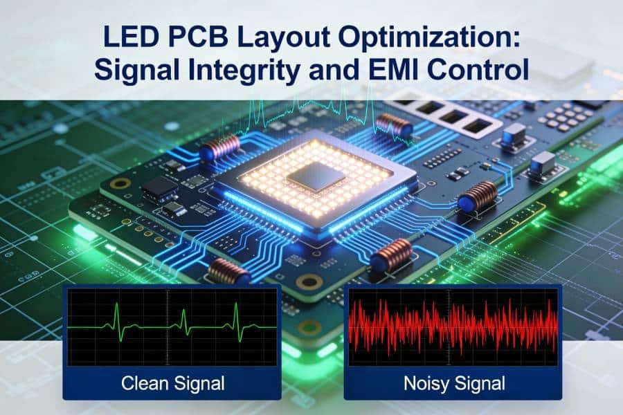
In high-density LED applications, PCB layout optimization is critical for preserving signal integrity and minimizing electromagnetic interference (EMI), ensuring reliable operation and regulatory compliance. Poor routing can cause crosstalk, ground bounce, and emissions exceeding CISPR 15 limits, while advanced techniques enable uniform light distribution and 30%+ efficiency gains. Explore our LED PCB Manufacturing & Assembly services for expert support.
Why Layout Matters for LED PCBs
LED circuits handle high current pulses from drivers (up to 2A peaks) and fast-switching PWM signals (kHz-MHz), making them prone to signal distortion and radiated EMI from long traces or poor grounding. Optimized layouts reduce return path inductance by 40-60%, prevent thermal crosstalk between LEDs, and support dense arrays in automotive, displays, and smart lighting.
LED PCB Layout Challenges
LED PCB layouts face unique challenges from high-current pulses, switching noise, and long traces that degrade signal integrity while generating EMI in dense arrays. These issues can cause 20-40% crosstalk, ground bounce exceeding 100mV, and emissions violating CISPR 15/EMC standards for lighting products.
Core Layout Challenges
- Signal Integrity Risks: PWM dimming (100Hz-20kHz) and DMX/DALI protocols suffer from ringing and overshoot on traces >50mm, amplified by 1-2A LED currents; poor returns increase inductance to 1nH/mm.
- EMI Generation Sources: Clock lines from MCUs, power planes switching at 50-500kHz, and LED arrays acting as antennas radiate 30-60dBμV/m in 150kHz-30MHz band.
- Thermal-Electrical Coupling: Adjacent high-power LEDs (>3W) create 15-25°C gradients, inducing resistance variation and noise via thermo-electric effects.
Unoptimized layouts reduce light uniformity by 15-30% and increase failure rates 2-3x in automotive/vibration environments.
Component Placement Strategies
LED PCB component placement forms the foundation of signal integrity and EMI control, dictating current flow, noise coupling, and thermal balance in dense lighting arrays. Strategic positioning minimizes trace lengths, isolates sensitive signals, and ensures uniform performance across high-power LEDs.
Key Placement Strategies
- Logical Grouping: Cluster high-current LEDs by driver channels to shorten power loops; place decoupling capacitors (<1mm from IC pins) to suppress 50-70% of transient noise.
- Signal Isolation: Separate digital control (MCU/DMX) from analog LED drivers by 5-10mm guard rings; orient traces perpendicular to reduce capacitive coupling by 25dB.
- Thermal Zoning: Stagger LED positions with 2-3mm spacing and interleaved ground vias to limit ΔT<10°C between chips, preventing current hogging in arrays.
For strip lights and panels, symmetric matrix placement with current-sharing resistors ensures <5% luminance variation.
Advanced Routing Techniques
Advanced routing techniques are essential for LED PCBs to maintain signal integrity under high-frequency PWM and control signals while suppressing EMI through controlled impedance and minimized loop areas. These methods reduce crosstalk by 30-50dB and ensure compliance with EMC standards like CISPR 15 for lighting products.
Essential Routing Techniques
- Differential Pair Routing: For DMX/DALI signals, maintain 100Ω impedance with equal-length pairs (tolerance <1mm), using L-shaped bends to cut loop inductance by 60%; space pairs 3x dielectric thickness from other traces.
- Power Plane Segmentation: Split analog ground (LED returns) from digital ground (MCU), connecting at single star-point near power entry; this eliminates 70-80% ground bounce.
- Short Trace Priority: Keep control signals <50mm, routing on inner layers with ground reference planes above/below; microstrip/stripline configurations yield 50Ω characteristic impedance.
Use 2-3oz copper pours for LED traces (>1mm width per amp), with stitched ground vias every 5mm.
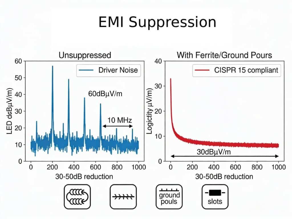
EMI Suppression Best Practices
EMI suppression techniques are vital for LED PCBs to meet stringent regulatory limits like CISPR 15 (150kHz-30MHz) and FCC Part 15, countering noise from switching drivers and high-current LED arrays. These practices reduce radiated emissions by 20-50dB, ensuring reliable operation in dense, high-power lighting systems.
| Technique | Application Area | EMI Reduction | Implementation Notes |
|---|---|---|---|
| Ferrite Beads | LED driver inputs/outputs | 30-50dB @ >10MHz | Select impedance 100-600Ω @ 100MHz; place <5mm from IC |
| Ground Copper Pours | Signal return paths | 20dB radiated EMI | Stitch vias every λ/20; full plane under traces |
| Guard Ring/Slots | Clock lines, sensitive signals | 15-25dB coupling | 1mm wide slots, grounded at both ends |
| Shielding Cans | MCU/control ICs | 40dB total enclosure | Seamless metal with GND vias |
| Spread Spectrum | PWM clock signals | 15dB peak reduction | 1-2% modulation on driver IC |
4-6 layer boards dedicate inner layers to solid GND planes for Faraday cage effects.
Verification and Testing
Verification of signal integrity and EMI performance is crucial to ensure LED PCBs meet EMC standards and deliver reliable operation in real-world conditions. Comprehensive testing validates advanced routing techniques, identifying issues like crosstalk or emissions early to avoid costly redesigns.
Essential Validation Methods
- Simulation Tools: Use HyperLynx or SIwave for 2.5D field solving to predict eye diagrams, insertion loss (<1dB @ 10MHz), and near-field EMI patterns before fabrication.
- Pre-Compliance Testing: Conduct radiated emissions scans (150kHz-1GHz) with spectrum analyzers, targeting <40dBμV/m at 3m per CISPR 15; LISN for conducted noise.
- Prototype Validation: Measure signal rise times (>1ns), ground bounce (<50mV), and thermal crosstalk via TDR/oscilloscope; AOI and flying probe for routing accuracy.
Functional testing under load verifies <5% current imbalance and uniform light output.
Conclusion
Mastering LED PCB layout optimization through strategic placement, advanced routing, and rigorous EMI control elevates designs to meet demanding automotive, commercial, and smart lighting requirements. These techniques reduce failure rates by 40% and accelerate time-to-market. Contact JHYPCB today for expert design review and get your optimized LED PCB Manufacturing & Assembly quote started.