Table of Contents
In the fast-paced world of electronics, turning a conceptual circuit diagram into a functional PCB layout is the bridge between innovation and real-world application. As a seasoned PCB manufacturer with over a decade of experience at JHYPCB, we’ve seen countless designs evolve from simple sketches to high-performance boards used in industries like automotive, medical devices, and consumer electronics. This process isn’t just about software tools—it’s about precision, foresight, and avoiding costly pitfalls that can derail your project.
Whether you’re a hobbyist prototyping a new gadget or an engineer scaling up for mass production, understanding how to convert circuit diagram to PCB layout is essential. In this in-depth guide, we’ll walk you through the steps with expert insights, drawing from our hands-on experience in PCB manufacturing and assembly services. We’ll cover everything from schematic design to Gerber file generation, while highlighting best practices to ensure your PCB is reliable, efficient, and ready for fabrication. At JHYPCB, we specialize in PCB prototype manufacturing, single-sided, double-sided, and multilayer PCBs, as well as rigid, flexible, and rigid-flex PCBs. Our PCB assembly services include SMT, THT, mixed technology, turnkey assembly, component sourcing, and SMT stencils—ensuring seamless transitions from design to delivery.
Why Converting Circuit Diagrams to PCB Layouts Matters
Before diving into the how-to, let’s consider the stakes. A poorly executed conversion can lead to signal integrity issues, thermal problems, or manufacturing defects, resulting in delays and increased costs. On the flip side, a well-optimized PCB layout enhances performance, reduces material waste, and speeds up time-to-market. Based on our projects at JHYPCB, we’ve found that investing time in this phase can cut rework by up to 50%. This guide will equip you with the knowledge to achieve that, incorporating long-tail keywords like “best practices for schematic to PCB layout conversion” and “tools for converting circuit diagram into PCB design” to help you navigate common challenges.

Step-by-Step Process: How to Convert Circuit Diagram to PCB Layout
Converting a circuit diagram into a PCB layout requires a systematic approach. We’ll expand on the basics with advanced tips from our engineering team, ensuring your design aligns with industry standards like IPC-7351 for footprints and IPC-2221 for trace routing.
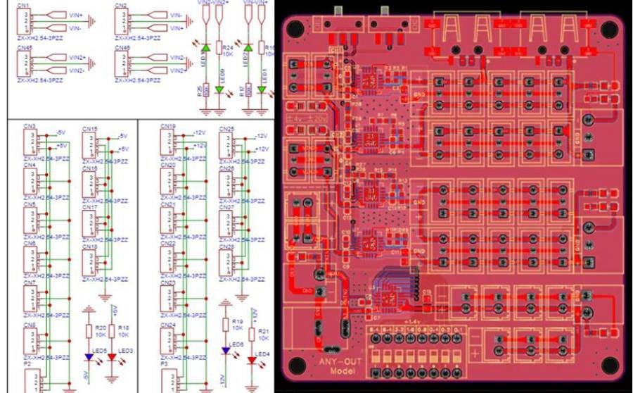
1. Circuit Schematic Design: The Foundation of Your PCB
Everything starts with a solid schematic. This isn’t just a drawing—it’s your blueprint that outlines components, connections, and electrical behaviors. Use tools like Altium Designer, KiCad, OrCAD, or Eagle to create it. Key elements include:
- Component Symbols and Values: Clearly label resistors, capacitors, ICs, and connectors with values, tolerances, and polarities.
- Net Labels and Hierarchies: Define power rails, ground planes, and signal paths to avoid confusion later.
- Simulation Integration: Run SPICE simulations to verify functionality before layout.
Pro Tip from JHYPCB: Always cross-reference your schematic against datasheets. We’ve encountered designs where mismatched pinouts led to assembly failures—double-check to save headaches during PCB prototype manufacturing.
2. Component Footprint Assignment: Matching Virtual to Physical
Once your schematic is ready, assign footprints. These are the physical representations of components on the board, dictating pad sizes, shapes, and spacing.
- Library Management: Use built-in libraries or create custom ones based on manufacturer specs. For instance, ensure SMD footprints comply with JEDEC standards.
- Variant Handling: Account for alternatives like through-hole vs. surface-mount versions.
At JHYPCB, we often advise clients on footprint optimization for our SMT assembly services. Choosing the right package can improve yield rates in high-volume production, especially for multilayer PCBs where space is premium.
3. PCB Outline Creation: Defining the Physical Boundaries
The outline sets the board’s shape and size, influenced by enclosure constraints, mounting points, and ergonomics.
- Form Factor Considerations: For compact devices, aim for irregular shapes with cutouts for connectors or sensors.
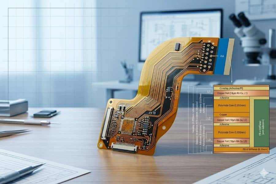
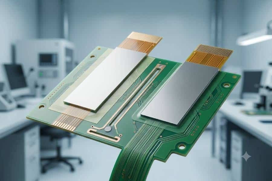
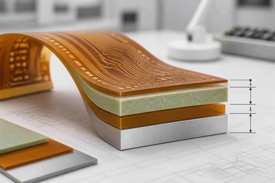
- Layer Stackup Planning: Decide on single-sided, double-sided, or multilayer early—multilayer is ideal for complex circuits to minimize size.
Expert Insight: Incorporate mechanical CAD data (e.g., STEP files) to ensure fit. In our rigid-flex PCB projects, precise outlines prevent flexing issues during use.
4. Component Placement: Optimizing for Functionality and Manufacturability
Placement is where theory meets reality. Arrange components to minimize trace lengths, reduce noise, and facilitate heat dissipation.
- Grouping Strategy: Cluster related components (e.g., power regulators near inputs) and separate analog from digital sections.
- Thermal and EMC Considerations: Place heat-generating parts away from sensitive ones; use thermal vias if needed.
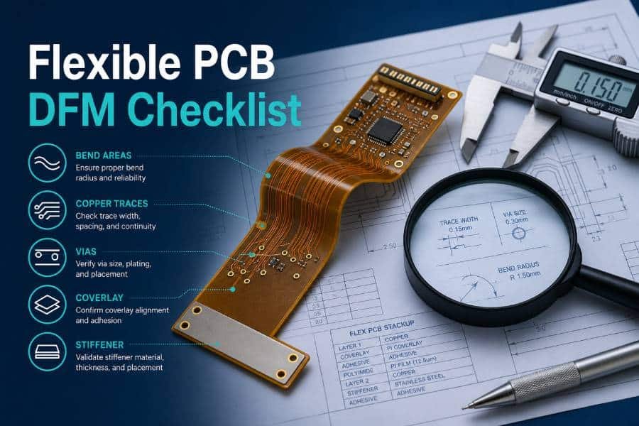
- DFM Checks: Ensure adequate spacing for assembly—our turnkey PCB assembly experience shows that 0.2mm minimum clearances boost reliability.
Long-Tail Tip: For “optimizing component placement in PCB layout design,” prioritize signal integrity by aligning high-speed traces straight and avoiding vias in critical paths.

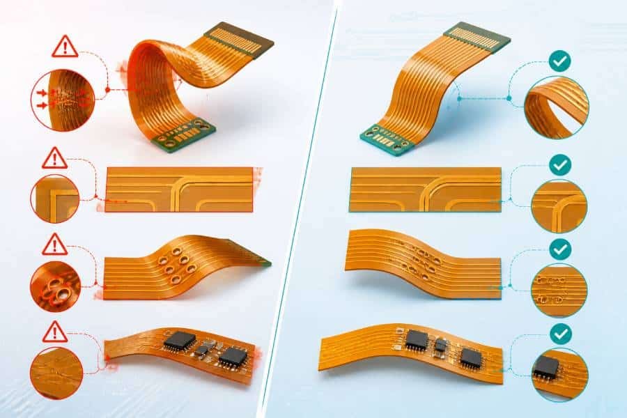
5. Traces Routing: The Backbone of Connectivity
Routing connects it all with copper traces, balancing electrical performance and board density.
- Trace Parameters: Calculate width based on current (use IPC-2152 charts) and impedance for controlled signals.
- Routing Techniques: Employ auto-routers for initial passes, then manual tweaks for optimization. Avoid 90-degree angles; use 45-degree or arcs instead.
- Differential Pairs and Length Matching: Crucial for USB, HDMI, or DDR interfaces.
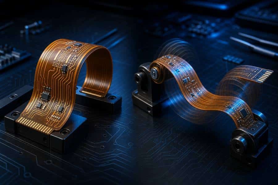
From JHYPCB’s Perspective: In flexible PCB manufacturing, route traces perpendicular to bend lines to prevent cracks. We’ve refined this in countless prototypes.
6. Addition of Vias and Planes: Enabling Multilayer Efficiency
For dense designs, go multilayer.
- Via Types: Through, blind, buried—choose based on layer transitions.
- Power/Ground Planes: Solid planes reduce EMI and provide low-impedance paths.
- Stitching Vias: Add them around planes for thermal relief and shielding.
Advanced Note: In rigid-flex PCBs, vias in flex areas need special reinforcement to handle bending stresses.
7. Design Rule Check (DRC) and Electrical Rule Check (ERC): Validation is Key
Run DRC to catch spacing violations, unconnected nets, or footprint errors. ERC verifies electrical consistency.
- Custom Rules: Set rules for your fab house—JHYPCB provides guidelines for our processes.
- 3D Preview: Use it to spot mechanical interferences.
We’ve prevented many issues by insisting on thorough checks before Gerber generation.

8. Gerber File Generation: Preparing for Manufacturing
Export your layout as Gerber files (RS-274X), including drill files, silkscreen, and solder mask layers.
- File Package: Include a README with specs like layer count and materials.
- CAM Review: Verify with tools like Gerbv.
At JHYPCB, we accept Gerber packages for quick quotes—email us at sales@pcbjhy.com for seamless PCB manufacturing and assembly.

Advanced Tips for Flawless PCB Layouts
To elevate your designs:
- Signal Integrity Analysis: Use tools like HyperLynx for simulations.
- Component Sourcing Early: Align with available parts to avoid redesigns—our component sourcing service can help.
- Eco-Friendly Practices: Minimize copper waste and choose lead-free options.
- Version Control: Track changes with Git-integrated tools.
- Common Pitfalls to Avoid: Overcrowding, ignoring thermal expansion, or forgetting test points.
Drawing from our expertise in mixed technology assembly, always prototype iteratively.
Conclusion: Elevate Your Designs with Professional Guidance
Mastering how to convert circuit diagram to PCB layout transforms ideas into reliable products. It’s a blend of creativity, engineering rigor, and practical know-how. At JHYPCB, we’ve supported thousands of projects with our comprehensive services, from PCB prototype to full turnkey assembly. If you’re ready to bring your design to life, contact us at sales@pcbjhy.com for expert advice and competitive quotes.
Remember, great PCBs start with great layouts—invest the time, and the results will speak for themselves.