Table of Contents
When designing PCBs, accurately conveying design data is critical for successful prototyping. Gerber files, the industry-standard format, are essential in this process. However, mistakes—big or small—can compromise prototype quality. What are the common pitfalls in Gerber file preparation? How can you ensure flawless output?
This guide provides a deep dive into Gerber file best practices, offering actionable insights for engineers and designers. We’ll cover:
- Choosing the right Gerber file format
- Understanding PCB layer types and their outputs
- Best practices for file naming
- Visual validation techniques
- Programmatic file integrity checks
- Submitting files to manufacturers
- Avoiding common errors with real-world examples
With expert tips, visual aids, and practical advice, this guide is your go-to resource for mastering Gerber files and achieving optimal PCB prototyping results.
Choosing the Right Gerber File Format
Selecting the appropriate Gerber file format from your CAD software is the first step toward successful PCB prototyping. The choice impacts compatibility and manufacturing efficiency.
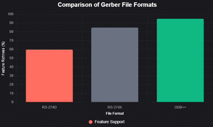
Historically, the RS-274D format, developed by Gerber Systems Corporation, used 2D vector coordinates to define PCB geometry, such as traces, pads, and holes. However, RS-274X, an enhanced version, has become the industry standard. It supports advanced features like step-and-repeat, regions, netlist data, and embedded component information, enabling manufacturers to optimize processes like laser drilling for high-density interconnects (HDI).
For cutting-edge designs, ODB++ offers even richer data integration, preserving native EDA tool structures. While ODB++ excels for complex multi-layer boards, RS-274X strikes a balance between universality and functionality, making it ideal for most applications.
Which format should you choose? For simple single- or double-layer boards, RS-274X is sufficient and widely supported. For advanced designs with HDI or microvias, ODB++ ensures better process optimization. The table below compares these formats:
Format | Feature Richness | Best Use Case | Compatibility |
|---|---|---|---|
RS-274D | Basic 2D geometry | Legacy equipment | High |
RS-274X | Enhanced metadata, step-and-repeat | General prototyping | Very High |
ODB++ | Native EDA data, complex designs | HDI, multi-layer boards | Moderate |
Understanding PCB Layer Types and Their Outputs
Gerber files represent various PCB design layers, each with distinct roles. Understanding their purpose and preparation is crucial for accurate prototyping.
Signal layers, such as copper and silkscreen, define circuit functionality and visual markings. Copper layers form conductive paths, while silkscreen layers display component outlines and labels.
Non-signal layers, like solder mask, outline, and drill layers, serve auxiliary roles. Soldermask protects copper traces, while outline layers define board boundaries and milling instructions.
A key concept is positive vs. negative polarity. Conductors and pads use positive polarity, while dielectric backgrounds use negative polarity to ensure precise layer rendering. Designers must also consider settings like minimum stroking width or clipping designs to the board profile to avoid visual errors.
Key Tip: Always verify layer settings in your CAD software to ensure correct polarity and output. Misconfigured layers can lead to manufacturing defects.
Best Practices for File Naming
Consistent file naming prevents mismatches during CAM processing. A robust naming schema should include:
- Board project name: Unique project identifier.
- Layer type: Specifies Top Copper, Bottom Soldermask, etc.
- Polarity: Indicates Positive or Negative.
- Revision: Tracks design versions (e.g., Rev2).
- Date: Provides a timestamp (e.g., YYYYMMDD).
Example: PCBPrototype_BottomCopper_Positive_Rev2_20231124
Additional guidelines:
- Use short names without special characters.
- Specify units (e.g., MM or INCH).
- Include author initials for traceability.
- Number inner layers sequentially.
The table below breaks down a sample naming structure:
Component | Example | Description |
|---|---|---|
Project Name | PCBPrototype | Unique project identifier |
Layer Type | BottomCopper | Specifies layer (e.g., Top Copper, Soldermask) |
Polarity | Positive | Indicates positive/negative plot |
Revision | Rev2 | Tracks design version |
Date | 20231124 | File creation date (YYYYMMDD) |
Adhering to these conventions ensures accurate layer stack-ups and prevents misplacements during fabrication.
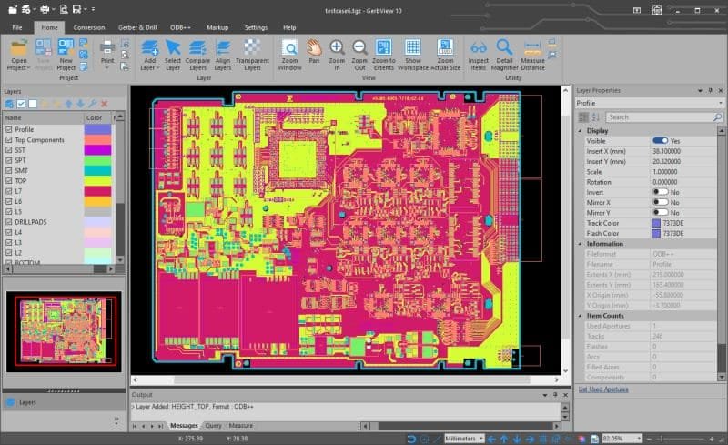
Ensuring Accuracy with Visual Validation
Before submitting Gerber files, visually validate layer alignments to catch errors. Tools like KiCad’s Gerber Viewer, Pentalogix ViewMate, or EasyEDA allow designers to overlay copper, solder mask, and silkscreen layers for sanity checks. Common issues include:
- Pads or vias not cleared of soldermask.
- Exposed copper not fully covered by mask.
- Component markings outside print bounds.
Advanced DFM tools, like JHYPCB’s Online DFM Check, automatically flag violations against manufacturing rules, ensuring error-free files.
Pro Tip: Perform a layer-by-layer review before exporting to ODB++ to confirm alignment and eliminate lingering issues.
Validating File Integrity
Visual checks catch obvious errors, but programmatic validation is essential for detecting subtle issues like polygon pours or connectivity breaks. Use CAD tools to perform:
- Electrical Rules Check (ERC): Verifies schematic-to-layout connectivity, flagging shorts, opens, or missing connections.
- Geometric Review: Ensures minimum spacing and component enclosure rules are met.
- Connectivity Verification: Confirms consistent net naming and electrical properties, especially for dense BGA/QFN packages.
- Layer Integrity Audits: Checks for correct layer content and boundary extents.
These audits ensure files align with your design intent, reducing costly prototype revisions.
Submitting Files to Your Manufacturer
Proper file packaging and transfer protocols streamline communication with your PCB manufacturer. Best practices include:
- Compress files: Bundle all Gerber files into a ZIP archive (e.g., ProductX_Rev2_GerberFiles.zip).
- Secure transfer: Use services like WeTransfer for reliable delivery and discuss checksums to verify file integrity.
- Versioning: Use sequential versioning (e.g., _V01, _V02) for iterative submissions.
- Include instructions: Provide a PIDX form detailing solder mask, surface finish, material types, and tolerances.
Learning from Common Gerber File Errors
Even experienced designers encounter Gerber file pitfalls. Common errors include:
- Missing layers: Omitting critical layers like drill files leads to incomplete prototypes.
- Incorrect polarity: Mislabeling positive/negative plots causes garbled routing.
- Excessive copper pours: Inadvertent polygon fills waste material and cause thermal stress. A 2023 study by a leading PCB manufacturer found that 15% of prototype rejections resulted from improper copper pours, delaying projects by 3-5 days on average.
Fiducial markers can also cause issues if they overlap active areas, creating visual defects post-soldermask application.
Lesson: Never skip visual and programmatic validation to avoid costly mistakes. Use tools like Altium Designer for robust checks.
Conclusion
Mastering Gerber file preparation is key to flawless PCB prototyping. By choosing the right format (e.g., RS-274X for most projects), understanding layer types, adopting consistent naming, and validating files thoroughly, you can ensure high-quality manufacturing outcomes. Avoid common errors with diligent checks and leverage tools like JHYPCB’s DFM Tool for added confidence.
As your trusted manufacturing partner, JHYPCB delivers fast, high-quality PCB prototyping backed by cutting-edge infrastructure. Let’s perfect your next project together!
Ready to Start Your PCB Project?
Get started with a free quote at JHYPCB Quote or contact us at sales@pcbjhy.com. For more PCB design resources, explore IPC Standards.
Related Reading