Table of Contents
Introduction
LED PCB design represents a unique engineering challenge that combines electrical circuit design with thermal engineering in ways that standard PCB design never demands. While designing circuit boards for microprocessors, sensors, or communication devices focuses primarily on signal integrity and electrical performance, LED PCB design elevates thermal management to equal—or even greater—importance. This fundamental shift in priorities catches many experienced PCB designers off guard, leading to products that work perfectly on the bench but fail catastrophically in the field.
The statistics tell a sobering story: industry studies estimate that 55-65% of LED product failures stem from thermal management issues rather than electrical defects. LEDs operating at excessive junction temperatures experience accelerated lumen depreciation, color shift, and shortened lifespan. A junction temperature just 20°C higher than specification can cut LED operational life in half. Yet these thermal failures are entirely preventable through proper PCB design techniques that manage heat as deliberately as electrons.
The challenge intensifies because LED PCB design mistakes reveal themselves slowly. Unlike electrical shorts that fail immediately during testing, thermal design inadequacies manifest over weeks or months of operation. By the time excessive junction temperatures cause visible light output degradation or premature failures, products have shipped to customers, warranties are in effect, and costly field issues multiply. Getting the design right the first time isn’t just best practice—it’s economic necessity.
This comprehensive guide provides the knowledge and techniques to design LED PCBs that deliver reliable, long-lasting performance. We’ll cover everything from initial LED selection and power calculations through advanced thermal simulation and design for manufacturing. Whether you’re designing your first LED circuit board or optimizing an existing product line, you’ll discover proven strategies for maximizing LED lifespan, ensuring uniform light output, and avoiding the costly pitfalls that plague poorly designed LED PCBs.
Understanding LED PCB Design Fundamentals
Before diving into specific design techniques, it’s essential to understand how LED PCB design differs philosophically from standard circuit board development.
Thermal Design as Primary Consideration
In standard PCB design, thermal management is often an afterthought—something addressed after routing is complete through strategic copper pours or external heat sinks. LED PCB design inverts this priority structure: thermal pathways must be engineered first, with electrical routing accommodating thermal requirements rather than the reverse.
Why This Matters:
LEDs convert only 30-40% of input electrical energy into light; the remaining 60-70% becomes heat that must be removed from the LED junction. For a 3-watt LED:
- Light output: ~1.2W (40% efficiency)
- Heat generation: ~1.8W
That 1.8 watts of thermal energy, concentrated in a 3-5mm² LED die, creates power densities exceeding 3000W per square inch—comparable to a kitchen stovetop burner. Without proper heat removal, junction temperatures rapidly exceed safe operating limits (typically 85-125°C depending on LED type), triggering the degradation cascade.
Thermal-First Design Philosophy:
- Calculate total heat dissipation requirements
- Select appropriate PCB substrate (aluminum, copper, or ceramic)
- Design thermal pathways (copper distribution, thermal vias)
- Plan heat sink integration or self-cooling approach
- Only then begin electrical routing within thermal framework
This sequence ensures thermal requirements receive attention they demand rather than being constrained by electrical layout decisions made without thermal consideration.
Electrical Design Requirements
While thermal management dominates LED PCB design, electrical considerations remain critical:
- Current Distribution:
LEDs require precise current regulation for consistent brightness and color. Circuit design must deliver specified current to each LED string with minimal variation (typically <5% LED-to-LED). - Voltage Management:
LED forward voltage varies with temperature and manufacturing tolerances. Designs must accommodate voltage variations (±10-15% typical) while maintaining current regulation. - Power Supply Integration:
LED driver placement affects both electrical performance and thermal management. Drivers generate heat themselves, requiring consideration in overall thermal budget. - Control Signals:
PWM dimming, color mixing, and smart controls introduce high-frequency signals requiring proper routing to prevent EMI and interference with LED performance.
Mechanical Design Considerations
Physical design aspects directly impact both electrical and thermal performance:
- Mounting and Attachment:
How the PCB mounts in the final product determines thermal interface options and mechanical stress on solder joints. - Dimensional Constraints:
Product housings may limit PCB thickness, shape, or area—constraining thermal design options. - Vibration and Shock:
Applications like automotive or industrial lighting demand robust mechanical design resistant to vibration fatigue. - Connector and Interface Placement:
Power input, control connections, and mounting holes must integrate with thermal design without creating thermal or electrical compromises.
The Interplay Between Thermal, Electrical, and Mechanical
Successful LED PCB design recognizes these three domains aren’t independent:
Thermal-Electrical Interactions:
- Copper used for heat spreading also carries current
- Thermal vias affect electrical impedance
- Hot spots influence circuit component placement
- Temperature affects LED forward voltage
Thermal-Mechanical Interactions:
- Heat sink attachment requires mechanical design
- Thermal expansion creates mechanical stress
- PCB thickness affects heat spreading
- Mounting methods impact thermal pathways
Electrical-Mechanical Interactions:
- Current-carrying traces need mechanical support
- Connector forces stress solder joints
- Vibration affects solder fatigue life
- Assembly processes constrain design options
Optimizing all three domains simultaneously requires holistic thinking and often involves trade-offs where improving one aspect slightly compromises another. Expert LED PCB design balances these competing requirements to achieve overall system optimization.
LED Selection and Power Calculations
LED PCB design begins not with CAD software, but with careful LED selection and accurate power calculations that establish thermal requirements.
Choosing the Right LEDs
LED selection profoundly impacts PCB design requirements. Key specifications to evaluate:
Power Requirements and Specifications
LED Power Rating:
LEDs range from milliwatts (indicator LEDs) to 100+ watts (high-power COB LEDs). Each power tier demands different PCB approaches:
- <0.5W: Standard FR4 PCB may suffice
- 0.5-3W: Aluminum MCPCB recommended
- 3-10W: Aluminum or copper core depending on density
- >10W: Copper core or ceramic substrate often required
Electrical Specifications:
- Forward Voltage (Vf): Typical value plus tolerance range (e.g., 3.0V ±0.3V)
- Forward Current (If): Rated current for specified lumen output
- Maximum Current: Absolute maximum before damage occurs
Thermal Specifications:
- Thermal Resistance (Rth j-c): Junction-to-case thermal resistance in °C/W
- Maximum Junction Temperature (Tj max): Typically 85-150°C depending on LED type
- Thermal Pad Specifications: Size and mounting requirements
Color Temperature and CRI Considerations
Color Temperature (CCT):
Measured in Kelvin (K), ranging from warm white (2700-3000K) through neutral white (4000-4500K) to cool white (5000-6500K).
Design Impact:
- Different CCTs may have different efficiency ratings
- Color temperature shifts with junction temperature
- Consistent thermal management ensures stable color output
Color Rendering Index (CRI):
CRI measures how accurately colors appear under LED illumination compared to natural light (CRI 100 = perfect).
Design Considerations:
- High-CRI LEDs (CRI >90) typically less efficient
- Generate more heat per lumen
- Premium applications justify thermal design investment
Voltage and Current Ratings
Forward Voltage Matching:
When connecting LEDs in series strings, forward voltage matching matters:
Example String Calculation:
- 10 LEDs × 3.2V nominal = 32V string voltage
- Vf tolerance ±10% = 28.8V to 35.2V range
- Driver must accommodate 6.4V variation
Binning Consideration:
Purchase LEDs from same manufacturing bin (tight Vf tolerances) when possible, simplifying driver design and improving LED-to-LED consistency.
Current Rating Selection:
LEDs can operate at various currents with corresponding output:
| Current (mA) | Relative Light Output | Relative Efficiency | Heat Generation |
|---|---|---|---|
| 350mA (typical) | 100% | 100% | Baseline |
| 500mA | 140% | 95% | +45% |
| 700mA | 180% | 90% | +100% |
| 1000mA | 240% | 85% | +180% |
Higher drive currents extract more light per LED but reduce efficiency and increase thermal challenges. Often more cost-effective to use additional LEDs at lower drive currents than fewer LEDs pushed to maximum ratings.
Power Dissipation Calculations
Accurate thermal calculations begin with understanding exactly how much heat each LED generates.
Electrical Power Input
Formula:
P_electrical = V_f × I_f
Where:
- Vf = Forward voltage at operating current
- If = Operating forward current
Example:
- LED: Vf = 3.2V @ If = 700mA
- P_electrical = 3.2V × 0.7A = 2.24W
Optical Efficiency
Not all electrical power converts to light—LED efficiency determines the split between optical output and heat:
Typical LED Efficiencies:
- Entry-level LEDs: 25-35% (65-75% becomes heat)
- Mid-range LEDs: 35-45% (55-65% becomes heat)
- Premium LEDs: 45-60% (40-55% becomes heat)
- Cutting-edge LEDs: 60-70% (30-40% becomes heat)
Efficiency varies with:
- LED technology and manufacturer
- Drive current (higher current = lower efficiency)
- Junction temperature (hotter = less efficient)
- Wavelength (blue more efficient than red)
Thermal Power Calculations
Formula:
P_thermal = P_electrical × (1 - Efficiency)
Example Calculation:
Given:
- P_electrical = 2.24W
- LED efficiency = 40% (typical mid-range)
Calculation:
P_thermal = 2.24W × (1 - 0.40)
P_thermal = 2.24W × 0.60
P_thermal = 1.34W per LED
This 1.34 watts represents heat that MUST be removed from the LED junction to prevent temperature rise.
Total Heat Dissipation Per LED
Conservative Design Approach:
Use worst-case assumptions for reliability:
- Assume lower efficiency bound (more heat)
- Account for efficiency reduction at elevated temperature
- Add safety margin (10-20%)
Revised Example:
P_thermal_design = P_electrical × (1 - Efficiency_min) × Safety_Factor
P_thermal_design = 2.24W × (1 - 0.35) × 1.15
P_thermal_design = 1.67W per LED
Designing for 1.67W instead of calculated 1.34W provides margin for manufacturing variations and operating condition uncertainties.
Array-Level Power Summation
Total PCB Thermal Load:
For LED arrays, sum individual LED heat dissipation:
Example: 20-LED Array
Total P_thermal = 20 LEDs × 1.67W/LED
Total P_thermal = 33.4W
Power Density:
Calculate watts per unit area:
Power Density = Total P_thermal / PCB Area
Example:
- Total thermal: 33.4W
- PCB dimensions: 200mm × 100mm = 20,000mm² = 200cm²
- Power Density = 33.4W / 200cm² = 0.167 W/cm² or 1.67 W/in²
Power Density Guidelines:
- <0.5 W/cm²: Aluminum MCPCB with natural convection often sufficient
- 0.5-1.5 W/cm²: Aluminum MCPCB with good thermal design required
- 1.5-3 W/cm²: Copper core MCPCB or forced air cooling
- >3 W/cm²: Specialized thermal solutions (ceramic, active cooling)
Junction Temperature Predictions
The ultimate goal of thermal calculations is predicting LED junction temperature under operating conditions.
Thermal Resistance Concepts
Thermal resistance (Rth) describes material resistance to heat flow, analogous to electrical resistance:
Formula:
ΔT = P × Rth
Where:
- ΔT = Temperature rise (°C)
- P = Power dissipated (W)
- Rth = Thermal resistance (°C/W)
Lower thermal resistance = better heat transfer = lower temperature rise.
Junction-to-Case Thermal Resistance (Rth j-c)
Specified by LED manufacturer, this value represents thermal resistance from LED junction (heat source) to LED package case (mounting surface to PCB).
Typical Values:
- Small SMD LEDs: 8-15 °C/W
- Mid-power LEDs: 5-10 °C/W
- High-power LEDs: 2-8 °C/W
- COB LEDs: 0.5-3 °C/W
Temperature Rise (Junction to Case):
ΔT_j-c = P_thermal × Rth_j-c
Example:
- P_thermal = 1.67W
- Rth_j-c = 6 °C/W
- ΔT_j-c = 1.67W × 6°C/W = 10°C
Case-to-Ambient Thermal Pathways
Heat must travel from LED case through multiple thermal resistances to reach ambient air:
Thermal Resistance Chain:
- LED Junction → LED Case: Rth_j-c (LED datasheet)
- LED Case → PCB Surface: Rth_c-pcb (solder joint, ~1-3 °C/W)
- PCB Surface → PCB Base: Rth_pcb (through dielectric layer)
- PCB Base → Heat Sink: Rth_interface (TIM, mounting, ~0.5-3 °C/W)
- Heat Sink → Ambient: Rth_h-a (heat sink performance)
Series Addition:
Rth_total = Rth_j-c + Rth_c-pcb + Rth_pcb + Rth_interface + Rth_h-a
Target Junction Temperature Limits
LED manufacturers specify maximum junction temperature (Tj_max), but optimal performance occurs well below this limit:
Design Guidelines:
| Application Type | Target Tj (°C) | Margin to Tj_max |
|---|---|---|
| Consumer products | <85°C | Moderate |
| Commercial lighting | <75°C | Conservative |
| Automotive/Industrial | <70°C | Very conservative |
| High-reliability/Military | <65°C | Extreme margin |
- Extends LED lifespan significantly
- Maintains stable color temperature
- Prevents lumen depreciation
- Accounts for ambient temperature variations
- Provides safety margin for manufacturing tolerances
Lifespan vs. Temperature Relationships
LED lifespan decreases exponentially with junction temperature:
Arrhenius Relationship:
Rule of thumb: Every 10°C increase in junction temperature cuts LED lifespan approximately in half.
Example Comparison:
| Junction Temp | Relative Lifespan |
|---|---|
| 65°C | 100,000+ hours |
| 75°C | 75,000 hours |
| 85°C | 50,000 hours |
| 95°C | 25,000 hours |
| 105°C | 12,500 hours |
Investing in better thermal management to reduce Tj from 95°C to 75°C can **triple LED lifespan**—often justifying significant investment in superior thermal design.
Cost-Benefit Analysis:
Assuming:
- LED cost: $2 per unit
- Product contains 20 LEDs: $40 in LED cost
- Better PCB thermal design: +$8 per unit
- Product warranty: 5 years
Scenario A: Adequate thermal design (Tj = 75°C)
- Expected LED failures over 5 years: 2-5% = 0.4-1 LED
- Warranty cost: Minimal
Scenario B: Poor thermal design (Tj = 95°C)
- Expected LED failures over 5 years: 15-25% = 3-5 LEDs
- Warranty cost: Replacement + labor + shipping + customer dissatisfaction
The $8 PCB investment prevents far greater warranty expenses while protecting brand reputation.
PCB Substrate Selection Strategy
With heat dissipation requirements quantified, selecting the optimal PCB substrate becomes a data-driven decision rather than guesswork.
Material Selection Decision Tree
Follow this systematic approach to substrate selection:
Step 1: Power Density Analysis
Calculate power density (from earlier calculations):
Decision Points:
- <0.3 W/cm²: FR4 potentially viable with excellent thermal design
- 0.3-0.8 W/cm²: Aluminum MCPCB recommended
- 0.8-2.0 W/cm²: Aluminum MCPCB with enhanced thermal design or copper core
- >2.0 W/cm²: Copper core or ceramic substrate likely required
Step 2: Ambient Temperature Considerations
Assess worst-case operating environment:
Temperature Ranges:
- Indoor controlled (20-30°C): Standard thermal solutions work
- Outdoor variable (-20 to 50°C): Need robust thermal margin
- Elevated ambient (40-70°C): Premium thermal substrates essential
- Extreme environments (>70°C or <-40°C): Ceramic often necessary
Ambient Temperature Impact on Substrate Choice:
| Ambient Temp | FR4 Max LED Power | Aluminum Recommended | Copper/Ceramic Required |
|---|---|---|---|
| <30°C | <0.5W | 0.5-5W | >5W |
| 30-50°C | <0.3W | 0.3-3W | >3W |
| 50-70°C | Not recommended | <2W | >2W |
| >70°C | Not recommended | Not recommended | All power levels |
Step 3: Lifespan Requirements
Match substrate selection to reliability expectations:
Short-term (<3 years / <20,000 hours):
- Cost optimization acceptable
- FR4 viable for low power
- Aluminum sufficient for most applications
Medium-term (3-7 years / 20,000-50,000 hours):
- Aluminum MCPCB standard choice
- Copper for high-power applications
- Conservative thermal design margins
Long-term (>7 years / >50,000 hours):
- Aluminum or copper with excellent thermal design
- Ceramic for mission-critical applications
- Maximum thermal safety margins
Step 4: Cost Constraints
Balance performance requirements with budget reality:
Budget Tiers:
- Ultra-low (<$3 PCB cost): FR4 only option; limit LED power severely
- Economy ($3-8): Aluminum MCPCB standard
- Mid-range ($8-20): Aluminum or copper depending on thermal needs
- Premium (>$20): Copper or ceramic for ultimate performance
Step 5: Application-Specific Factors
Consider unique requirements:
Vibration/Shock Environment:
- Metal core rigidity benefits automotive, industrial
- Ceramic brittleness concern in shock environments
Weight Constraints:
- Aluminum lightweight (2.7 g/cm³)
- Copper heavy (8.96 g/cm³) – aerospace concern
- Consider aluminum even if thermal limits marginal
Size Limitations:
- Smaller boards limit thermal spreading
- May require premium substrate despite lower total power
Regulatory Requirements:
- UL, CE, automotive standards
- May mandate specific substrate types or thermal margins
For comprehensive substrate comparison and selection guidance, see our detailed article: 6 Types of LED PCB Boards.
Aluminum vs Copper vs Ceramic: When to Use Each
Understanding when each substrate type provides optimal value:
When Aluminum MCPCB Suffices
Ideal Conditions:
- Individual LED power: 0.5-5W
- Power density: 0.3-1.5 W/cm²
- Ambient temperature: <50°C with good airflow
- Target lifespan: 30,000-75,000 hours
- Cost-conscious applications
- Commercial and consumer products
Aluminum Advantages:
- Excellent cost-to-performance ratio
- Wide supplier availability
- Short lead times (5-10 days typical)
- Proven reliability across applications
- Lightweight for automotive/portable products
Thermal Performance:
- Thermal conductivity: 1-2 W/mK (through dielectric)
- Adequate for 80% of LED applications
- Supports natural convection cooling for moderate power
When Aluminum Reaches Limits:
- Junction temperatures approach or exceed 85°C
- Power density requires forced air cooling
- Ambient temperatures regularly exceed 50°C
- Application demands extreme longevity (>100,000 hours)
When Copper Core Becomes Necessary
Compelling Use Cases:
- Individual LED power: >5W per component
- Power density: >1.5 W/cm²
- High ambient temperature: >50°C typical
- Compact form factor: Limited PCB area for heat spreading
- Extended lifespan: >75,000-100,000 hours required
- Performance-critical: Automotive headlights, stage lighting, industrial
Copper Core Advantages:
- Thermal conductivity: 3-8 W/mK (2-4x aluminum performance)
- Handles extreme power densities
- Superior heat spreading capability
- Lower CTE (17-18 ppm/°C) reduces thermal stress
- Extended LED lifespan through better thermal management
Copper Core Trade-offs:
- Cost: 2-3x aluminum pricing
- Weight: 3.3x heavier than aluminum
- Oxidation: Requires protective coatings
- Supplier availability: Fewer qualified manufacturers
- Lead time: Typically 2-4 weeks
Decision Point:
If thermal analysis shows aluminum can’t maintain junction temperature <80-85°C under worst-case conditions, copper core justifies its premium cost through improved reliability and lifespan.
When Ceramic Justifies Cost
Specialized Applications:
- Ultra-high power: >10W per LED
- Extreme environments: Temperature >100°C or <-40°C
- Mission-critical: Aerospace, military, medical
- Chemical exposure: Harsh industrial environments
- Maximum lifespan: >100,000 hours required
- Optical stability: Precise thermal stability needed
Ceramic Options:
Aluminum Oxide (Al₂O₃) – More Common:
- Thermal conductivity: 20-30 W/mK
- Cost: 5-10x aluminum MCPCB
- Good balance of performance and cost
- Suitable for most premium applications
Aluminum Nitride (AlN) – Ultimate Performance:
- Thermal conductivity: 150-180 W/mK (approaches copper metal)
- Cost: 15-20x aluminum MCPCB
- Unmatched thermal performance
- Reserved for extreme requirements
Ceramic Advantages:
- Highest thermal conductivity available
- Superior electrical insulation (10-20 kV/mm)
- Extreme temperature capability (-55°C to +350°C)
- Excellent CTE matching to LEDs (4-7 ppm/°C)
- Chemical inertness and corrosion resistance
- Longest possible LED lifespan
Ceramic Limitations:
- Very high cost (often $50-$200+ per board)
- Brittle – susceptible to mechanical shock/impact
- Complex manufacturing – limited suppliers
- Long lead times (4-8 weeks typical)
- Difficult to rework or modify
When Ceramic Makes Sense:
- Thermal analysis shows copper insufficient
- Operating environment exceeds metal core capabilities
- Product failure consequences severe (safety, replacement difficulty)
- Market positioning justifies premium costs
- Regulatory requirements demand maximum reliability
Hybrid Substrate Approaches
Sometimes the optimal solution combines multiple substrate types strategically:
Common Hybrid Configurations:
FR4 Control Section + Aluminum LED Section:
- Complex control electronics on economical FR4
- High-power LEDs on aluminum thermal section
- Single integrated assembly
- Optimizes cost vs. performance
Aluminum Standard LEDs + Copper High-Power LED Zones:
- Most LEDs on aluminum substrate
- Hot spot LEDs (high power) on embedded copper zones
- Balances cost with targeted thermal management
Benefits:
- Cost optimization: Premium materials only where needed
- Design flexibility: Complex circuits + thermal management
- Performance: Right substrate for each function
Considerations:
- Manufacturing complexity increases cost somewhat
- Requires suppliers capable of hybrid fabrication
- Longer lead times than single-substrate boards
- More complex thermal simulation required
Dielectric Layer Specifications
The dielectric layer—bonding copper circuit layer to metal base—critically determines LED PCB thermal performance.
Thermal Conductivity Ratings
Dielectric thermal conductivity directly affects heat transfer from LEDs to metal base:
Performance Tiers:
| Thermal Conductivity | Classification | Typical Cost | Applications |
|---|---|---|---|
| 0.8-1.2 W/mK | Standard | Baseline | Low-medium power LEDs |
| 1.5-2.5 W/mK | Enhanced | +20-40% | Medium power LEDs |
| 3.0-5.0 W/mK | High Performance | +50-80% | High power LEDs |
| >5.0 W/mK | Premium | +100%+ | Extreme power density |
For 3W LED on aluminum base:
- 1.0 W/mK dielectric: ~15°C temperature rise through dielectric
- 3.0 W/mK dielectric: ~5°C temperature rise through dielectric
- 10°C improvement can extend LED lifespan 30-50%
Thickness Options and Trade-offs
Dielectric layer thickness affects both thermal and electrical performance:
Standard Thicknesses:
- 50μm: Best thermal performance, adequate electrical isolation for <48V
- 75μm: Balanced thermal/electrical, suitable for most applications
- 100μm: Enhanced electrical isolation, suitable for 48-120V
- 150μm: High-voltage applications (>120V), reduced thermal performance
- 200μm: Maximum electrical isolation, significantly impacts thermal transfer
Trade-off Analysis:
Thinner Dielectric:
- ✅ Better thermal performance (lower thermal resistance)
- ✅ Lower temperature rise
- ❌ Reduced electrical isolation
- ❌ Higher risk of dielectric breakdown
- ❌ Lower voltage capability
Thicker Dielectric:
- ✅ Better electrical isolation
- ✅ Higher breakdown voltage rating
- ✅ Safer for high-voltage applications
- ❌ Worse thermal performance
- ❌ Higher junction temperatures
- ❌ May negate metal core benefits
Selection Guidelines:
| LED Voltage | Recommended Dielectric Thickness | Considerations |
|---|---|---|
| <24V DC | 50-75μm | Optimize thermal performance |
| 24-48V DC | 75-100μm | Balance thermal and electrical |
| 48-120V | 100-150μm | Electrical safety priority |
| >120V | 150-200μm | Maximum isolation required |
Electrical Insulation Requirements
Dielectric must provide adequate electrical isolation despite conducting heat:
Key Specifications:
Dielectric Breakdown Voltage:
- Standard: >3000V
- Enhanced: >4000V
- Premium: >5000V
Safety Margin:
Design for 10x operating voltage minimum:
- 48V LED system → 480V minimum breakdown voltage → Standard dielectric adequate
- 120V LED system → 1200V minimum → Standard still adequate with margin
Insulation Resistance:
- Minimum: >10¹² Ω·cm
- Prevents leakage currents
- Critical for safety certification (UL, CE)
Material Vendors and Options
Several specialized materials dominate LED PCB dielectric layers:
Common Dielectric Materials:
Bergquist (Henkel):
- Industry leader in thermal interface materials
- HiFlow™ series: 1.0-2.0 W/mK
- T-preg™ series: 2.0-3.0 W/mK
Laird Performance Materials:
- Tflex™ thermal interface materials
- TPCM (Thermal Phase Change Material) options
- 1.5-4.0 W/mK range
Dowa (Japan):
Specialized metal core PCB die
lectrics
- High thermal conductivity options
- 2.0-5.0 W/mK specialized formulations
Practical Note:
Most LED PCB designers specify dielectric performance requirements (thermal conductivity, thickness, breakdown voltage) rather than specific material brands. Manufacturers select appropriate materials meeting specifications from qualified suppliers.
Thermal Management Design
Thermal management represents the heart of LED PCB design. This section covers critical techniques ensuring LEDs operate within safe temperature limits.
Copper Weight and Distribution
Copper layers serve dual purposes: conducting electricity AND spreading heat. Optimizing copper distribution dramatically improves thermal performance.
1oz vs 2oz vs 3oz Copper Selection
Copper Weight Specifications:
- 1oz copper: 35μm (1.4 mil) thickness – standard PCB default
- 2oz copper: 70μm (2.8 mil) thickness – 2x thermal performance
- 3oz copper: 105μm (4.2 mil) thickness – 3x thermal performance
Thermal Impact:
Copper thermal conductivity: 385 W/mK (excellent)
Heat Spreading Comparison:
- 1oz copper: Baseline thermal spreading
- 2oz copper: ~80% better heat spreading (not quite 2x due to 3D heat flow)
- 3oz copper: ~150% better heat spreading
Cost Impact:
- 1oz to 2oz: +10-20% PCB cost
- 2oz to 3oz: +15-30% additional cost
Design Recommendation:
For LED PCBs, 2oz copper is the sweet spot for most applications:
- Significantly better thermal performance than 1oz
- Moderate cost increase
- Widely available from manufacturers
- Handles LED power up to 3-5W per component
Use 3oz copper when:
- Individual LEDs exceed 5W
- Power density very high (>2 W/cm²)
- Compact design limits spreading area
- Maximum thermal performance needed
Copper Pour Maximization Strategies
Solid Copper Fills:
Maximize continuous copper areas around LEDs:
Best Practices:
- Fill all unused board area with copper (top layer)
- Extend copper pours as close to board edges as manufacturing rules allow
- Connect all copper areas to form continuous thermal plane
- Minimize breaks and gaps in copper
Thermal Benefit:
Large continuous copper areas spread heat effectively before it enters dielectric layer. The more copper surface area, the lower the thermal resistance.
Example:
- LED thermal pad: 10mm × 10mm = 100mm²
- Extended copper pour: 50mm × 50mm = 2,500mm²
- 25x larger heat spreading area = dramatically lower temperature rise
Solid vs Hatched Fills
Solid Fills (Recommended for LED PCBs):
- Continuous copper with no gaps
- Maximum thermal conductivity
- Best heat spreading
- Minimal thermal resistance
Hatched/Meshed Fills:
- Copper grid pattern with gaps
- Reduces copper usage (cost saving)
- Poor thermal performance (gaps block heat flow)
- NOT recommended for LED thermal management areas
Rule: Use solid copper fills for all LED thermal zones. Hatched fills may be acceptable only in non-thermal areas if cost reduction is critical.
Copper Thickness Impact on Thermal Performance
Quantitative Analysis:
For 3W LED on aluminum MCPCB:
| Copper Weight | Thermal Resistance | Temperature Rise | Relative Cost |
|---|---|---|---|
| 1oz (35μm) | ~12°C/W | 36°C | Baseline |
| 2oz (70μm) | ~8°C/W | 24°C | +15% |
| 3oz (105μm) | ~6°C/W | 18°C | +30% |
Result: Upgrading 1oz to 2oz copper reduces LED temperature by 12°C—potentially doubling LED lifespan—for just 15% cost increase.
Design Decision: 2oz copper should be default specification for LED PCBs unless budget absolutely prohibits.
Thermal Via Design
Thermal vias conduct heat vertically through the PCB, creating critical thermal pathways from LEDs to the metal core substrate.
Via Size and Quantity Calculations
Standard Thermal Via Specifications:
- Diameter: 0.3-0.5mm (12-20 mil) typical
- Plating: Standard copper plating
- Spacing: 0.8-1.5mm center-to-center
- Pad diameter: Via diameter + 0.2-0.3mm
Thermal Via Effectiveness:
Single via thermal resistance: ~50-150°C/W (depends on diameter, length, plating)
Multiple Vias in Parallel:
Rth_total = Rth_single / Number_of_vias
Example:
- Single via: 100°C/W
- 8 vias in array: 100°C/W ÷ 8 = 12.5°C/W
- Significant thermal improvement
How Many Vias Needed?
General Guidelines:
| LED Power | Recommended Thermal Vias | Pattern |
|---|---|---|
| <1W | 4-6 vias | Simple array under LED |
| 1-3W | 6-12 vias | Dense array covering thermal pad |
| 3-5W | 12-20 vias | Full coverage + extensions |
| >5W | 20+ vias | Maximum density allowed by design rules |
Placement Optimization:
- Center vias directly under LED thermal pad
- Distribute evenly across thermal pad area
- Extend via array slightly beyond LED footprint
- Maintain manufacturer’s minimum via-to-via spacing
Placement Strategies Under LED Pads
Optimal Via Pattern:
LED Thermal Pad (example: 10mm × 10mm)
○ ○ ○ ○ ○ ○ = Thermal via (0.3-0.5mm)
○ ○ ○ ○ ○ Spacing: 1.0-1.5mm
○ ○ ○ ○ ○ Pattern: Grid or staggered
○ ○ ○ ○ ○ Total: 20 vias
○ ○ ○ ○ ○
Design Rules:
- Position vias to avoid solder wicking during reflow (leave center area for solder)
- Maintain minimum distance from via edge to pad edge (0.2mm typical)
- Use solder mask to cover vias when possible
- Consider via plugging/capping to prevent solder wicking
Advanced Pattern:
For high-power LEDs (>5W), extend thermal via array beyond LED footprint into surrounding copper pour:
Extend via field 5-10mm beyond LED in all directions
Creates larger effective heat transfer zone
Reduces thermal bottleneck at LED interface
Via Filling vs Capping
Open Vias (Standard):
- Copper-plated holes remain open
- Most economical
- Adequate for most applications
- Risk: Solder wicking during assembly
Via Plugging/Filling:
- Vias filled with conductive or non-conductive epoxy
- Prevents solder wicking
- Creates flat surface for LED mounting
- Better thermal contact
- Additional cost: +$0.50-$2 per board
Via Capping (Tenting):
- Solder mask covers via openings
- Prevents solder migration
- Less effective than filling
- Standard option, no cost premium
Recommendation:
- Standard applications: Use capped vias (solder mask over)
- High-reliability: Specify via filling for flat LED mounting surface
- Ultra-high-power: Conductive epoxy via filling for maximum thermal transfer
Thermal Via Array Patterns
Grid Pattern:
- Vias arranged in regular rectangular grid
- Easy to design and manufacture
- Uniform thermal distribution
- Most common approach
Staggered Pattern:
- Alternating rows offset by half spacing
- Slightly higher via density possible
- Marginal thermal improvement
- More complex to design
Concentric Pattern:
- Vias arranged in circular rings around center
- Matches circular LED die geometry
- Aesthetic appeal
- No significant thermal advantage over grid
Recommendation: Use simple grid pattern for ease of design and manufacturing unless specific geometric requirements dictate otherwise.
Effectiveness Analysis
Thermal Via Impact Example:
3W LED on 2oz copper aluminum MCPCB:
| Configuration | Thermal Resistance | Junction Temp (50°C ambient) |
|---|---|---|
| No thermal vias | ~15°C/W | 95°C |
| 4 thermal vias | ~10°C/W | 80°C |
| 12 thermal vias | ~7°C/W | 71°C |
| 20 thermal vias | ~6°C/W | 68°C |
Diminishing Returns:
Note that going from 12 to 20 vias provides only 3°C additional improvement. There’s an optimal point where adding more vias provides minimal benefit.
Design Guideline:
Calculate via density providing 80-90% of maximum possible thermal improvement. Beyond this point, cost and design complexity outweigh marginal gains.
LED Placement and Spacing
Strategic LED positioning prevents thermal interaction and hot spots while optimizing optical performance.
Minimum Spacing Requirements
LEDs generate thermal zones extending beyond their physical footprint. Insufficient spacing causes thermal crosstalk where heat from adjacent LEDs elevates junction temperatures.
Thermal Interaction Zone:
Each LED creates a temperature gradient in the PCB extending ~15-30mm radius from LED center, depending on power level and substrate type.
Minimum Spacing Guidelines:
| LED Power | Minimum Edge-to-Edge Spacing | Center-to-Center Distance |
|---|---|---|
| <0.5W | 10mm | 15-20mm |
| 0.5-1W | 15mm | 20-25mm |
| 1-3W | 20mm | 30-40mm |
| 3-5W | 30mm | 45-60mm |
| >5W | 40mm+ | 60mm+ |
Exceptions:
Tighter spacing acceptable when:
- Substrate is copper core (better spreading)
- Excellent heat sinking (direct chassis mount)
- LEDs don’t operate simultaneously at full power
- Thermal simulation confirms acceptable temperatures
Thermal Interaction Zones
Heat Spreading Radius:
Estimate thermal influence zone:
Thermal Zone Radius ≈ 10 × √(LED_Power_Watts)
Examples:
- 1W LED: ~10mm thermal zone radius
- 3W LED: ~17mm thermal zone radius
- 5W LED: ~22mm thermal zone radius
Design Rule:
Space LEDs such that their thermal zones minimally overlap. Significant overlap causes each LED’s temperature to be elevated by heat from neighbors.
Staggered vs Grid Patterns
Grid Pattern (Aligned Rows/Columns):
○ ○ ○ ○
○ ○ ○ ○
○ ○ ○ ○
Advantages:
- Simple, intuitive layout
- Easy to design and verify spacing
- Uniform appearance
- Standard for most applications
Disadvantages:
- Some thermal interaction in rows/columns
- Less optimal thermal distribution
Staggered Pattern (Offset Rows):
○ ○ ○ ○
○ ○ ○
○ ○ ○ ○
Advantages:
- Better thermal distribution
- Reduces direct alignment thermal interactions
- Can achieve higher LED density
- Optimal for high-power applications
Disadvantages:
- More complex design
- May complicate optical designs
Recommendation:
- Standard power (<2W): Grid pattern adequate
- High power (>2W): Consider staggered for better thermal management
- Optical requirements often dictate pattern regardless of thermal preferences
Edge Clearances
LEDs near board edges have less copper area for heat spreading:
Design Rules:
- Minimum edge clearance: 10-15mm from LED center to board edge
- Preferred clearance: 20-30mm for high-power LEDs
- Corner placement: Avoid placing high-power LEDs near corners (two edges limiting heat spread)
Edge LED Design:
If LEDs must be near edges:
- Increase copper thickness (2oz → 3oz)
- Add extra thermal vias
- Consider external heat sink contact near edge
- Route thermal pathways toward board interior
Hotspot Avoidance
Common Hotspot Causes:
- Clustered LEDs: Multiple LEDs too close together
- Limited copper area: Insufficient heat spreading space
- Inadequate thermal vias: Bottleneck at LED interface
- Poor heat sink contact: Ineffective thermal escape path
- Board center accumulation: Heat trapped in center with no escape
Prevention Strategies:
- Use thermal simulation to identify hot spots before fabrication
- Distribute high-power LEDs around periphery when possible
- Ensure thermal pathways to heat sink or board edges
- Balance LED placement for uniform temperature distribution
- Monitor center-of-board temperatures (often hottest area)
For detailed thermal simulation guidance, see our advanced guide: Thermal Management in LED PCB.
Heat Spreading Techniques
Beyond copper pours and thermal vias, advanced heat spreading techniques optimize thermal pathways across the entire PCB.
Copper Plane Design
Strategic copper plane design maximizes lateral heat spreading before heat enters the dielectric layer.
Continuous Thermal Planes:
Best Practice:
- Create uninterrupted copper planes covering maximum board area
- Extend copper from LED thermal zones toward board edges
- Connect all copper areas into single thermal network
- Minimize breaks for routing – use vias to jump obstacles
Multi-Zone Thermal Design:
For boards with multiple LED clusters:
[LED Cluster A] ← Thermal Plane → [Central Area] ← Thermal Plane → [LED Cluster B]
Design Strategy:
- Create thermal superhighways between LED zones and heat sinks
- Use wide copper bridges (10-20mm) connecting thermal zones
- Avoid narrow thermal pathways that create bottlenecks
- Balance copper distribution for uniform temperature
Copper Plane Thickness Impact:
| Feature | 1oz Copper | 2oz Copper | 3oz Copper |
|---|---|---|---|
| Lateral spreading | Baseline | +80% better | +150% better |
| Thermal mass | Low | Medium | High |
| Heat capacity | Quick response | Moderate | High inertia |
| Cost premium | Baseline | +15% | +30% |
Thermal Pathways Engineering
Design deliberate thermal pathways from heat sources to heat sinks:
Pathway Planning:
- Identify heat sources: Map LED locations and power levels
- Identify heat sinks: Board edges, mounting points, external heat sinks
- Create thermal corridors: Design copper pathways connecting sources to sinks
- Minimize thermal resistance: Maximize pathway width and copper thickness
Thermal Corridor Design:
Example Layout:
[LED Array]
↓ (Wide copper pour 20mm+)
[Thermal Via Field]
↓ (Through dielectric to metal base)
[Metal Base Spreading]
↓ (Thermal interface material)
[Heat Sink/Chassis]
Width Guidelines:
- LED to thermal via field: Match LED thermal pad width minimum
- Thermal corridor: 15-30mm width for high-power paths
- Edge approach: Gradually widen toward heat sink contact area
Thermal Impedance Minimization:
Calculate thermal resistance of each pathway segment:
Rth_pathway = Rth_copper + Rth_vias + Rth_dielectric + Rth_base + Rth_interface
Optimize each component:
- Copper: Maximize thickness and area
- Vias: Increase quantity, reduce spacing
- Dielectric: Specify high thermal conductivity material
- Base: Copper core if aluminum insufficient
- Interface: High-quality thermal pads or grease
Multiple Heat Sink Attachment Points
For large LED arrays or high-power applications, multiple heat sink attachment points distribute thermal load:
Multi-Point Mounting Strategy:
Single Heat Sink (Standard):
- PCB mounts at center or one edge
- Heat must conduct to mounting area
- Effective for compact boards (<100cm²)
Multi-Point Heat Sink:
- PCB mounts at multiple locations (corners, edges)
- Distributes thermal load across attachment points
- Reduces peak temperatures
- Optimal for large boards (>200cm²)
Design Considerations:
- Place high-power LEDs near mounting points when possible
- Ensure thermal pathways to all mounting locations
- Use thermal interface material at all contact points
- Design for uniform clamping pressure across all points
Attachment Point Optimization:
| Board Size | Attachment Points | Max Distance from LED to Mount |
|---|---|---|
| <50cm² | 1 central | <50mm |
| 50-150cm² | 2-3 points | <75mm |
| 150-300cm² | 4-6 points | <100mm |
| >300cm² | 6+ points | <125mm |
Distribute LED power across attachment points:
- Calculate heat dissipation per mounting zone
- Balance LED placement to equalize thermal load
- Avoid concentrating high-power LEDs in one area
- Use thermal simulation to verify load distribution
Thermal Interface Planning
The junction between PCB and external surfaces critically affects overall thermal performance.
Direct PCB-to-Chassis Contact:
Best Practice for Maximum Performance:
- Mount PCB metal base directly to aluminum chassis/housing
- Use thin thermal interface material (0.1-0.5mm)
- Ensure flat mounting surfaces (flatness tolerance <0.1mm)
- Apply uniform clamping pressure across entire contact area
Thermal Interface Material (TIM) Selection:
Will be covered in detail in next section on Heat Sink Integration.
Contact Area Maximization:
Design Strategies:
- Maximize PCB area in direct contact with heat sink
- Remove solder mask from bottom of metal core (improves thermal contact)
- Use mounting screws or clips to ensure consistent pressure
- Consider adhesive thermal pads for permanent mounting
Thermal Gap Management:
Air gaps devastate thermal transfer:
- 0.1mm air gap: Adds ~10-20°C/W thermal resistance
- Poor surface flatness: Creates random air pockets
- Inadequate clamping: Allows gaps at edges
Solutions:
- Specify chassis/heat sink flatness tolerance
- Use compliant thermal pads that fill gaps
- Design adequate mounting pressure (2-5 psi typical)
- Consider thermal gap-filling materials for uneven surfaces
Heat Sink Integration
For LED PCBs exceeding ~15-30W total power, external heat sink integration becomes necessary.
Heat Sink Selection Criteria
Choosing appropriate heat sinks balances thermal performance, cost, size, and weight.
Thermal Performance Requirements:
Calculate required heat sink thermal resistance:
Rth_heatsink = (Tj_target - T_ambient) / P_total - Rth_LED_to_case - Rth_PCB - Rth_interface
Example:
- Target junction temp: 75°C
- Ambient temp: 50°C
- Total LED power: 30W
- LED + PCB + interface resistance: 3°C/W
Required heat sink resistance:
Rth_heatsink = (75 - 50) / 30 - 3 = 0.83 - 3 = **Negative!**
This indicates PCB self-cooling insufficient; external heat sink mandatory.
Recalculate with realistic Tj:
Allow Tj = 85°C
Rth_heatsink = (85 - 50) / 30 - 3 = 1.17 - 3 = Still negative
Indicates need for forced air cooling or larger heat sink with active cooling.
Heat Sink Types:
Extruded Aluminum:
- Most common and cost-effective
- Standard profiles readily available
- Thermal resistance: 1-10°C/W depending on size
- Natural or forced convection
Die-Cast Aluminum:
- Custom shapes and complex geometries
- Integrated mounting features
- Good for product housings serving as heat sinks
- Higher tooling costs but good for volume
Stamped/Folded Metal:
- Low cost for high volumes
- Limited thermal performance
- Suitable for low-power applications
Machined/Skived Fin:
- Highest performance (thin, dense fins)
- Expensive but maximum cooling
- Used for extreme power density
Thermal Resistance Guidelines:
| Heat Sink Type | Natural Convection | Forced Air (200 LFM) |
|---|---|---|
| Small extruded (50cm²) | 8-12°C/W | 3-5°C/W |
| Medium extruded (150cm²) | 3-6°C/W | 1.5-3°C/W |
| Large extruded (300cm²) | 1.5-3°C/W | 0.8-1.5°C/W |
| Custom high-performance | 1-2°C/W | 0.5-1°C/W |
Attachment Methods
Securing PCB to heat sink affects both thermal and mechanical performance.
Screw Mounting (Most Common):
Advantages:
- Reliable mechanical attachment
- Controllable clamping pressure
- Easy disassembly for service
- Excellent thermal contact with proper TIM
Best Practices:
- Use 3-6 mounting screws depending on board size
- Torque screws to specification (0.5-1.5 N⋅m typical)
- Use wave washers for consistent pressure
- Stagger screw tightening (star pattern) for uniform pressure
Screw Spacing:
- Maximum screw spacing: 80-120mm for uniform clamping
- Place screws near high-power LED zones when possible
- Ensure even pressure across entire contact area
Clip Mounting:
Advantages:
- No through-holes in PCB required
- Quick assembly/disassembly
- Good for prototypes and low-volume production
Considerations:
- Clips must provide adequate clamping force
- Risk of uneven pressure distribution
- Ensure clips don’t block LED light output
- Verify clips maintain pressure over temperature cycling
Adhesive Mounting:
Thermal Adhesive Tapes:
- Permanent attachment
- No fasteners required
- Uniform pressure across entire area
- Simplifies assembly
Types:
- 3M 8810, 8815 (thermally conductive acrylic adhesive)
- Pressure-sensitive adhesive (PSA) with thermal conductivity 0.6-1.5 W/mK
- Typical thickness: 0.1-0.5mm
Advantages:
- Simplest assembly process
- No mechanical fasteners or holes
- Excellent for compact designs
- Good for vibration resistance
Limitations:
- Permanent (difficult to rework)
- Moderate thermal performance vs. screws with paste
- Requires clean, flat surfaces
- Temperature limitations (typically <150°C)
Adhesive Selection Criteria:
- Thermal conductivity: >0.8 W/mK minimum
- Bond strength: >1 MPa for secure attachment
- Temperature range: Exceeds max operating temp
- Thickness: As thin as possible (0.1-0.25mm preferred)
Thermal Interface Materials (TIM)
The material between PCB and heat sink critically affects thermal transfer.
TIM Types and Characteristics:
Thermal Grease/Paste:
- Thermal conductivity: 1-8 W/mK
- Thickness: 0.05-0.15mm (very thin layer)
- Best performance: Highest thermal conductivity options
- Application: Requires careful spreading, messy
- Rework: Easy to clean and reapply
- Cost: Low (pennies per application)
Recommended for: Prototype, low-volume, maximum thermal performance
Thermal Pads (Gap Fillers):
- Thermal conductivity: 1-6 W/mK
- Thickness: 0.5-3.0mm (fills larger gaps)
- Compliance: Conforms to surface irregularities
- Application: Clean, easy, no mess
- Rework: Remove and replace pads
- Cost: Moderate ($0.50-$3 per board)
Recommended for: Production, automated assembly, varying gap sizes
Phase Change Materials (PCM):
- Thermal conductivity: 2-4 W/mK
- Operation: Solid at room temp, softens at ~45-50°C
- Benefits: Combines ease of pad with performance of grease
- Application: Applied like pad, flows like grease when hot
- Cost: Moderate to high
Recommended for: High-reliability, automotive, long-term installations
Thermal Adhesive Tapes:
- Thermal conductivity: 0.6-2.0 W/mK
- Function: Bonding + thermal transfer
- Benefits: No mechanical fasteners needed
- Limitations: Lower thermal performance than paste
- Cost: Moderate
Recommended for: Permanent attachment, compact designs
TIM Selection Matrix:
| Application | Recommended TIM | Thermal Conductivity | Application Method |
|---|---|---|---|
| Prototype/Testing | Thermal grease | 3-8 W/mK | Manual application |
| Low-volume production | Thermal pads | 2-5 W/mK | Manual placement |
| High-volume automated | Thermal pads or adhesive | 1-4 W/mK | Automated dispense/placement |
| Maximum performance | Thermal grease | 5-8 W/mK | Careful manual application |
| Permanent installation | Thermal adhesive tape | 0.8-2 W/mK | PSA application |
| High reliability | Phase change material | 2-4 W/mK | Pre-applied, activates with heat |
Contact Area Optimization
Maximizing effective contact area between PCB and heat sink reduces thermal resistance.
Surface Preparation:
PCB Bottom Surface:
- Remove solder mask from metal base contact area (if manufacturer allows)
- Specify smooth finish (no texture)
- Ensure flatness tolerance <0.1mm across contact area
- Clean surface before TIM application (isopropyl alcohol)
Heat Sink Surface:
- Machine flat contact surface (flatness <0.05mm ideal)
- Smooth finish (Ra < 1.6μm) for best thermal grease contact
- Slightly rougher OK for thermal pads (they conform)
- Remove anodization from contact area if thermally resistive
Contact Area Calculation:
Effective contact area = actual PCB/heat sink overlap × contact quality factor
Contact Quality Factors:
- Perfect contact with thin grease: 0.95-0.98
- Good contact with thermal pad: 0.85-0.92
- Moderate contact (some air gaps): 0.70-0.80
- Poor contact (uneven surfaces): 0.50-0.65
Maximizing Effective Contact:
Design PCB outline to match or exceed heat sink base size
- Use maximum PCB thickness practical (better rigidity, less bowing)
- Apply uniform clamping pressure across entire contact area
- Use multiple mounting points for large contact areas (>100cm²)
- Consider heat sink base thickness (thicker = flatter = better contact)
Pressure Distribution:
Inadequate or uneven pressure creates air gaps:
Optimal Mounting Pressure:
- Too low (<0.5 psi): Incomplete contact, air gaps, poor thermal transfer
- Optimal (2-5 psi): Good contact, TIM spreads properly, no damage
- Too high (>10 psi): Risk of PCB damage, component stress, minimal thermal benefit
Achieving Uniform Pressure:
Screw Mounting:
Torque Specification = Force / (Screw Count × Contact Area)
Example:
- Desired pressure: 3 psi
- Contact area: 20 cm² = 3.1 in²
- Required force: 3 psi × 3.1 in² = 9.3 lbs
- 4 mounting screws
- Force per screw: 9.3 / 4 = 2.3 lbs
- Convert to torque based on screw size and thread pitch
Practical Approach:
- Use torque screwdriver or torque-limiting screws
- Tighten in star pattern (diagonal sequence)
- Re-torque after initial settling
- Verify with pressure-sensitive film if critical
Area Coverage Efficiency:
Calculate effective thermal contact:
Effective_Area = Physical_Contact_Area × Surface_Quality_Factor × Pressure_Distribution_Factor
Optimization Strategies:
- Maximize physical overlap between PCB and heat sink
- Improve surface flatness (machining, lapping)
- Use compliant TIM that fills microscopic gaps
- Ensure adequate and uniform clamping pressure
- Avoid warped PCBs or heat sinks (manufacturing quality control)
Verification Methods:
During Development:
- Thermal imaging of assembled unit under load
- Thermocouple measurements at multiple contact points
- Infrared thermography showing temperature uniformity
- Pressure-sensitive film confirming even pressure distribution
In Production:
- Junction temperature testing on sample units
- Thermal resistance measurements
- Visual inspection of TIM spread pattern (when disassembled)
- Automated thermal testing for high-volume production
For expert guidance on heat sink selection, TIM specification, and thermal interface optimization for your specific LED application, consult our Technical Capabilities team. We provide thermal analysis, heat sink design recommendations, and validation testing services.
Electrical Design Best Practices
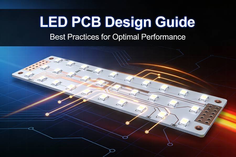
While thermal management dominates LED PCB design, proper electrical design ensures consistent LED performance, uniform brightness, and reliable operation.

LED Circuit Topologies
How LEDs connect electrically affects performance, efficiency, and failure modes.
Series Strings
Configuration:
(+) → LED1 → LED2 → LED3 → ... → LEDn → (-)
Characteristics:
- All LEDs carry identical current
- Total voltage = Sum of individual LED forward voltages
- Single current path through entire string
- One LED failure opens circuit (all LEDs extinguish)
Advantages:
- Current uniformity: All LEDs receive identical current, ensuring uniform brightness
- Simple driver design: Single constant-current driver for entire string
- Efficient: No current-balancing resistors wasting power
- Cost-effective: Fewer driver components required
Disadvantages:
- High voltage: Long strings require high-voltage drivers (potentially >100V)
- Single point of failure: One open LED kills entire string
- Vf matching critical: Forward voltage variations affect string voltage
- Limited flexibility: Cannot dim individual LEDs independently
Design Guidelines:
String Length Calculation:
Max LEDs per string = (Driver_Vmax - Headroom) / LED_Vf_typical
Example:
- Driver max voltage: 48V
- Required headroom: 3V
- LED Vf: 3.2V typical
- Max LEDs: (48 – 3) / 3.2 = 14 LEDs per string
String Voltage Planning:
String_Vmin = LEDs_per_string × LED_Vf_min
String_Vmax = LEDs_per_string × LED_Vf_max
Example with 10 LEDs (Vf = 3.0-3.4V):
- Minimum string voltage: 10 × 3.0V = 30V
- Maximum string voltage: 10 × 3.4V = 34V
- Driver must accommodate 30-34V range
Best Applications:
- High-voltage LED systems (automotive 12V/24V, commercial 48V+)
- Long LED strips
- Applications requiring maximum efficiency
- When uniform brightness is critical
Parallel Arrays
Configuration:
(+)
|
┌────┼────┬────┐
| | | |
LED1 LED2 LED3 LEDn
| | | |
└────┼────┴────┘
|
(-)
Characteristics:
- All LEDs see identical voltage
- Current divides among parallel LEDs
- Multiple current paths
- One LED failure doesn’t affect others (but increases current through remaining LEDs)
Advantages:
- Low voltage: Operates at single LED forward voltage (~3V)
- Redundancy: Individual LED failures don’t disable entire array
- Flexible: Easy to add or remove LEDs
- Simple voltage supply: Standard 3.3V or 5V supplies work
Disadvantages:
- Current sharing issues: LED Vf variations cause unequal current distribution
- Thermal runaway risk: Hottest LED draws more current, gets hotter, draws even more current
- Requires current balancing: Resistors or active circuits needed per LED
- Lower efficiency: Balancing resistors waste power
- Brightness variations: LEDs may have unequal brightness
Current Sharing Problem:
LEDs with slightly lower Vf draw more current:
- LED A: Vf = 3.0V → draws 25mA (brighter)
- LED B: Vf = 3.2V → draws 18mA (dimmer)
- LED C: Vf = 3.1V → draws 21mA (medium)
Solutions:
Individual Current Limiting Resistors:
(+) Vsupply
|
┌───┼───┬───┐
R R R R (Current limiting resistor per LED)
| | | |
LED LED LED LED
| | | |
└───┼───┴───┘
|
(-)
Resistor Calculation:
R = (Vsupply - LED_Vf) / LED_If
Example:
- Supply: 5V
- LED: Vf = 3.2V, If = 20mA
- R = (5 – 3.2) / 0.02 = 90Ω
- Use standard value: 91Ω or 100Ω
Power Dissipation:
P_resistor = (Vsupply - Vf) × If = 1.8V × 0.02A = 0.036W
Efficiency Loss:
Efficiency = LED_Power / Total_Power = (3.2V × 0.02A) / (5V × 0.02A) = 64%
36% of power wasted in resistor!
Best Applications:
- Low-voltage systems (3.3V, 5V supplies)
- Small LED counts (<10 LEDs)
- Indicator lights and status displays
- When redundancy is critical
- Prototyping and testing
Series-Parallel Combinations
Configuration:
(+)
|
┌─────┼─────┐
| |
LED1→LED2 LED3→LED4 (Series strings)
| |
└─────┼─────┘
|
(-)
(Parallel connection of series strings)
Characteristics:
- Multiple series strings connected in parallel
- Combines advantages of both topologies
- Most common configuration for LED arrays
- Balances voltage requirements with current sharing
Advantages:
- Moderate voltage: Lower than pure series (better safety, driver availability)
- Better redundancy: String failure doesn’t kill entire array
- Improved current sharing: Fewer parallel paths to balance
- Design flexibility: Optimize string length for available driver voltage
- Good efficiency: Fewer balancing components than pure parallel
Disadvantages:
- String balancing needed: Series strings may draw unequal current
- More complex design: Must balance both series and parallel considerations
- Multiple failure modes: Open LED or shorted LED affect differently
Design Approach:
Step 1: Determine String Length
Based on available driver voltage:
LEDs_per_string = (Driver_Voltage - Headroom) / LED_Vf
Step 2: Calculate Number of Strings
Based on total LED count:
Number_of_strings = Total_LEDs / LEDs_per_string
Step 3: String Current Balancing
Each string needs current regulation or balancing:
Method A: Separate drivers per string (best performance)
Driver1 → String1 (LED1→LED2→LED3)
Driver2 → String2 (LED4→LED5→LED6)
Driver3 → String3 (LED7→LED8→LED9)
Method B: Single driver with string balancing resistors
Driver (+)
|
┌───────┼───────┬───────┐
R1 R2 R3 R4 (Small balancing resistors)
| | | |
String1 String2 String3 String4
| | | |
└───────┼───────┴───────┘
|
Driver (-)
Resistor sizing:
- Create ~0.5-1V drop across resistor
- R = 0.5V / String_current
- Reduces efficiency but improves current sharing
Method C: Active current regulation per string (premium)
- Use current regulator IC per string
- Perfect current matching
- Higher cost but optimal performance
Example Design:
Requirements:
- 24 LEDs total
- LED: Vf = 3.2V, If = 350mA
- Available driver: 24V, 1.4A
Design:
LEDs per string = (24V - 3V) / 3.2V = 6 LEDs
Number of strings = 24 / 6 = 4 strings
Current per string = 350mA
Total current = 4 × 350mA = 1.4A ✓ (matches driver)
Configuration:
(+24V)
|
├─(LED1→LED2→LED3→LED4→LED5→LED6)─┐
├─(LED7→LED8→LED9→LED10→LED11→LED12)─┤
├─(LED13→LED14→LED15→LED16→LED17→LED18)─┤
└─(LED19→LED20→LED21→LED22→LED23→LED24)─┘
|
(Driver -)
Best Applications:
- Medium to high-power LED arrays (>10W)
- Commercial and architectural lighting
- Automotive lighting systems
- Any application requiring >10 LEDs
- Balance between voltage/current requirements
Current Balancing Requirements
Ensuring uniform current across all LEDs prevents brightness variations and hot spots.
Why Current Balancing Matters:
Vf Variation Impact:
- LED manufacturing: ±5-10% Vf variation typical
- Temperature effects: Vf decreases ~2mV/°C
- Aging: Vf drifts over lifetime
Without Balancing:
- 10% Vf variation → 30-50% current variation in parallel LEDs
- Brightness visibly uneven
- Hot LEDs age faster (positive feedback loop)
- Thermal runaway possible
Balancing Methods Comparison:
| Method | Performance | Efficiency | Cost | Best For |
|---|---|---|---|---|
| Series strings | Excellent | Excellent | Low | High voltage OK |
| Resistor per LED | Good | Poor (60-80%) | Low | Low voltage, few LEDs |
| Resistor per string | Good | Good (85-92%) | Low | Series-parallel arrays |
| Linear regulators | Excellent | Moderate (75-85%) | Medium | Medium precision needed |
| Active current reg | Outstanding | Good (85-92%) | High | Premium applications |
Design Recommendation:
Low-power indicator LEDs: Individual resistors acceptable
Medium-power arrays (<20W): Series-parallel with string resistors
High-power arrays (>20W): Separate constant-current drivers per string or active regulation
Premium applications: Active current regulation for each LED/string
Trace Width Calculations
Properly sized traces ensure current-carrying capacity and minimize voltage drop and heating.
Current Carrying Capacity
PCB traces have maximum current limits before excessive heating occurs.
Factors Affecting Current Capacity:
- Trace width
- Copper thickness (weight)
- Copper temperature rating
- Ambient temperature
- Internal vs external layer
- Adjacent heat sources
IPC-2152 Standards
Modern standard replacing outdated IPC-2221 provides accurate current capacity calculations.
Key Improvements Over IPC-2221:
- Accounts for copper thickness accurately
- Considers trace cross-sectional area
- More conservative and safer
- Based on extensive empirical testing
IPC-2152 Formula (Simplified):
Current (A) = k × ΔT^0.44 × A^0.725
Where:
- k = constant (depends on internal/external layer)
- ΔT = Allowed temperature rise (°C)
- A = Cross-sectional area (mils²)
Practical Approach – Use Lookup Tables:
External Traces (Top/Bottom Layer), 2oz Copper:
| Trace Width | Max Current (10°C rise) | Max Current (20°C rise) |
|---|---|---|
| 0.25mm (10mil) | 0.7A | 1.0A |
| 0.5mm (20mil) | 1.3A | 1.9A |
| 1.0mm (40mil) | 2.4A | 3.5A |
| 2.0mm (80mil) | 4.5A | 6.5A |
| 3.0mm (120mil) | 6.5A | 9.3A |
| 5.0mm (200mil) | 10.5A | 15A |
Note: 1oz copper values approximately 0.7× these values
For LED PCBs:
- Use 2oz copper minimum for power traces
- Target temperature rise <10°C for reliability
- Build in 20-30% safety margin
Temperature Rise Considerations
Excessive trace heating causes multiple problems in LED PCBs.
Problems from Hot Traces:
- Voltage drop increases (copper resistance rises with temperature)
- Nearby components heat up
- Solder joints weaken
- Trace itself adds to overall thermal budget
- Potential solder reflow damage (>183°C for lead-free)
Temperature Rise Guidelines:
Conservative Design (Recommended for LED PCBs):
- Maximum trace temperature rise: 10°C above ambient
- Provides safety margin for current surges
- Prevents trace contribution to LED heating
- Ensures stable voltage delivery
Standard Design:
- Temperature rise: 10-20°C acceptable
- Most general electronics use this range
- Adequate for moderate-reliability applications
Aggressive Design (Not recommended for LEDs):
- Temperature rise: 20-40°C
- Minimal copper usage
- Risk of reliability issues
- Only for cost-critical, short-life products
Calculation Example:
LED string requiring 700mA:
- Ambient: 50°C
- Allowed rise: 10°C
- Max trace temp: 60°C
Using 2oz copper, external trace:
- From table: 0.5mm trace handles 700mA with ~8°C rise ✓
- Design choice: Use 1.0mm trace for margin
- Actual rise: ~4°C
- Provides 100% current margin (could handle 1.4A)
Voltage Drop Minimization
Voltage drop in traces reduces voltage available to LEDs, affecting brightness and performance.
Voltage Drop Calculation:
V_drop = I × R_trace
Where:
R_trace = ρ × L / A
- ρ = Copper resistivity (1.72 × 10⁻⁸ Ω⋅m at 20°C)
- L = Trace length (m)
- A = Cross-sectional area (m²)
Simplified Formula for PCB Traces:
R_trace (mΩ) = 0.5 × L(mm) / [W(mm) × T(oz)]
Where:
- L = Trace length in mm
- W = Trace width in mm
- T = Copper thickness in oz (1oz = 35μm)
Example Calculation:
- Trace: 100mm long, 1mm wide, 2oz copper
- Current: 700mA
Resistance:
R = 0.5 × 100 / (1 × 2) = 25mΩ = 0.025Ω
Voltage drop:
V_drop = 0.7A × 0.025Ω = 0.0175V = 17.5mV
For 3.2V LED, this represents 0.55% drop – acceptable.
Acceptable Voltage Drop Guidelines:
| Application | Max Voltage Drop | Typical Target |
|---|---|---|
| LED power traces | <2% of LED Vf | <1% preferred |
| Driver to LED | <100mV | <50mV ideal |
| Long LED strips | <3% end-to-end | Design for <2% |
Voltage Drop Minimization Strategies:
1. Increase Trace Width:
- Double width → half resistance → half voltage drop
- Cost: Minimal board area
- Benefit: Significant drop reduction
2. Increase Copper Weight:
- 1oz → 2oz: Half the resistance
- 2oz → 3oz: 33% reduction
- Cost: Moderate PCB cost increase
- Benefit: Better thermal and electrical performance
3. Shorten Trace Length:
- Place LED driver close to LED array
- Route power traces directly (avoid meandering)
- Use both sides of board for power routing if needed
4. Use Power Planes:
- Solid copper pour for power distribution
- Much lower resistance than narrow traces
- Excellent for multi-LED arrays
5. Kelvin Sensing (for critical applications):
- Separate sense lines to measure actual LED voltage
- Driver compensates for trace drop
- Ensures precise LED voltage regulation
Design Example – Long LED Strip:
Requirements:
- 20 LEDs in series string
- LED: 3.2V @ 350mA
- Strip length: 300mm
- String voltage: 64V
Analysis:
- Trace length: 300mm
- Current: 350mA
- Trace: 2mm wide, 2oz copper
Resistance: R = 0.5 × 300 / (2 × 2) = 37.5mΩ
Voltage drop: V = 0.35A × 0.0375Ω = 13mV
Percentage: 13mV / 64V = 0.02% ✓ Excellent
If using 0.5mm trace (inadequate):
R = 0.5 × 300 / (0.5 × 2) = 150mΩ
V_drop = 0.35 × 0.15 = 52.5mV
Percentage: 52.5mV / 64V = 0.08% – Still acceptable but uses design margin
Recommendation: Use 1.5-2mm minimum trace width for LED power distribution.
Online Calculators and Tools
Several free tools simplify trace width calculations:
Popular Trace Width Calculators:
1. CircuitCalculator.com PCB Trace Width Calculator
- Implements IPC-2152 standards
- Inputs: Current, temperature rise, copper weight, trace length
- Outputs: Minimum width, resistance, voltage drop
- Free, no registration required
2. Saturn PCB Design Toolkit
- Professional-grade calculator
- Advanced features: multilayer, differential pairs
- Free download for Windows
- Industry standard tool
3. 4PCB Trace Width Calculator
- Simple web-based interface
- IPC-2221 and IPC-2152 options
- Instant results
- Mobile-friendly
4. DigiKey Online Calculator
- Integrated with component search
- Saves calculations with projects
- Tutorial and reference materials included
Usage Workflow:
Step 1: Determine requirements
- LED current (include all LEDs on trace)
- Maximum trace length
- Copper weight (1oz or 2oz typically)
- Allowed temperature rise (use 10°C for LEDs)
Step 2: Input to calculator
- Run calculation for initial width
- Check voltage drop
- Verify within acceptable limits
Step 3: Add design margin
- Increase calculated width by 20-30%
- Round up to convenient dimension
- Verify manufacturable (>0.15mm minimum)
Step 4: Document decision
- Record calculations in design documentation
- Note any assumptions or safety factors
- Include for design reviews
Best Practice:
Calculate trace widths for all power-carrying traces before PCB layout. Create design rules in CAD software enforcing minimum widths automatically.
Power Distribution Planning
Systematic power distribution design ensures stable voltage delivery to all LEDs with minimal losses.
Power Supply Placement
LED driver location affects trace lengths, voltage drop, and thermal management.
Placement Considerations:
Close to LED Array:
- Advantages:
- Minimizes power trace lengths
- Reduces voltage drop
- Simplifies routing
- Disadvantages:
- Driver heat near LED thermal zones
- Limited placement flexibility
- May complicate assembly
Separate from LED Array:
- Advantages:
- Isolates driver heat from LED thermal zones
- Allows driver placement in cooler areas
- Easier thermal management
- Disadvantages:
- Longer power traces required
- Higher voltage drop potential
- More complex routing
Design Guidelines:
For Low-Power Systems (<10W):
- Driver placement less critical
- Place for convenient assembly
- Keep within 100mm of LED array
For Medium-Power (10-30W):
- Consider thermal implications
- Place driver away from high-power LEDs
- Keep power traces <150mm
- Use 2oz copper for power routing
For High-Power (>30W):
- Mandatory thermal separation
- Driver in coolest board area
- Heat sink for driver if needed
- Wide power traces (2-5mm) or power planes
- Consider separate driver board
Multi-Zone LED Arrays:
For designs with multiple LED zones:
Driver 1 → LED Zone A (Front lighting)
Driver 2 → LED Zone B (Side lighting)
Driver 3 → LED Zone C (Rear lighting)
Benefits:
- Independent control per zone
- Reduced current per power trace
- Better fault isolation
- Simpler thermal management
Distribution Network Design
How power routes from driver to LEDs affects performance and reliability.
Star Topology (Recommended for <10 LEDs):
Driver
|
┌─────┼─────┬─────┐
| | | |
LED1 LED2 LED3 LED4
Advantages:
- Equal trace length to each LED
- Uniform voltage drop
- No cascading current effects
- Simplest troubleshooting
Disadvantages:
- Requires more board area
- More complex routing
- Only practical for small LED counts
Daisy Chain Topology (Common for LED Strips):
Driver → LED1 → LED2 → LED3 → ... → LEDn
Advantages:
- Simple, linear routing
- Minimal board area
- Natural for strip lights
Disadvantages:
- Cumulative voltage drop
- Last LED sees most drop
- Current flows through all connections
- Brightness may vary end-to-end
Mitigation:
- Size traces for cumulative current
- Consider dual-feed (power from both ends)
- Calculate worst-case voltage drop
Hybrid Topology (Best for Large Arrays):
Driver
|
Power Bus (wide trace or plane)
|
┌───┼───┬───┼───┐
| | |
Zone1 Zone2 Zone3
(Series (Series (Series
LEDs) LEDs) LEDs)
Advantages:
- Combines star and daisy benefits
- Scalable to large LED counts
- Manageable voltage drop
- Zones can be independently controlled
Design Approach:
- Main Power Bus: Wide trace (3-5mm) or power plane from driver
- Zone Branches: Individual traces to LED zones
- Local Distribution: Series strings within each zone
- Return Path: Adequate ground return (match power trace width)
Decoupling Capacitor Placement
Capacitors stabilize power delivery, reduce noise, and improve LED performance.
Purpose of Decoupling:
- Filter high-frequency switching noise from LED drivers
- Provide local energy storage for LED turn-on transients
- Stabilize voltage during current changes
- Reduce EMI and radiated noise
Capacitor Selection:
Bulk Capacitance (Driver Output):
- Value: 100-470μF electrolytic or ceramic
- Voltage rating: 1.5× maximum operating voltage minimum
- Placement: Close to LED driver output (<25mm)
- Purpose: Smooth switching ripple, energy storage
Local Decoupling (Per LED Zone):
- Value: 10-47μF ceramic (X7R or X5R dielectric)
- Voltage rating: 1.5× zone voltage
- Placement: Within 10mm of first LED in zone
- Purpose: Local transient response
High-Frequency Filtering:
- Value: 0.1-1.0μF ceramic (X7R)
- Placement: Immediately adjacent to each LED cluster
- Purpose: Filter high-frequency noise
Placement Best Practices:
Rule 1: Close to Power Pins
Place capacitors as close as possible to the pins they’re decoupling – within 5-10mm for small capacitors, <25mm for bulk caps.
Rule 2: Short Traces
Use short, wide traces to capacitor pads. Long, thin traces add inductance reducing effectiveness.
Rule 3: Via Placement
Place vias immediately adjacent to capacitor pads when connecting to power planes, not under pads.
Rule 4: Multiple Small > One Large
Use several smaller capacitors distributed across board rather than single large cap in one location.
Example Decoupling Scheme:
30W LED Array with 4 Zones:
Zone 1 (8W):Driver Output:
└─ 220μF/50V electrolytic (bulk)
└─ 10μF/50V ceramic (local to driver)
└─ 22μF/25V ceramic
└─ 0.1μF per LEDZone 2 (8W):
└─ 22μF/25V ceramic
└─ 0.1μF per LED
Zone 3 (7W):
└─ 22μF/25V ceramic
└─ 0.1μF per LED
Zone 4 (7W):
└─ 22μF/25V ceramic
└─ 0.1μF per LED
Ground Plane Strategies
Proper ground design ensures stable reference and low-impedance return paths.
Ground Plane Design:
Single-Point Ground (Small Systems):
- All grounds connect to single point
- Avoids ground loops
- Good for <10W LED systems
- Simple but requires careful layout
Ground Plane (Recommended for LED PCBs):
- Solid copper pour on bottom layer (or top if single-sided)
- Provides low-impedance return path
- Excellent for thermal spreading (bonus)
- Connect driver ground and all LED grounds to plane
- Use multiple vias for low impedance
Split Ground Planes (Advanced):
- Separate analog and digital grounds (if using microcontroller/sensors)
- Connect at single point (star ground)
- Prevents digital noise coupling to LEDs
- Only for complex LED control systems
Best Practices:
Maximize Ground Plane Area:
- Fill all unused board area with ground plane
- Connect all ground plane islands
- No floating copper areas
Adequate Return Current Paths:
- Ground return traces should match power trace width
- Current flows in both directions
- Inadequate ground causes unexpected voltage drop
Via Stitching:
- Use multiple ground vias connecting layers
- Space vias every 20-40mm
- Creates low-inductance ground connection
- Helps with EMI reduction
Keep Ground Plane Continuous:
- Avoid breaks or slots in ground plane
- Route signals around ground plane, not through it
- Breaks increase return path length and impedance
Current Limiting and Protection
Protecting LEDs from over-current and transients ensures reliable operation.
Resistor-Based Current Limiting
Simple, passive current control suitable for low-power applications.
Basic Configuration:
Vsupply → Resistor → LED → Ground
Resistor Calculation:
R = (Vsupply - LED_Vf) / LED_If
Power Dissipation:
P_resistor = (Vsupply - LED_Vf) × LED_If
Example:
- Supply: 12V
- LED: Vf = 3.2V, If = 350mA
- R = (12 – 3.2) / 0.35 = 25.1Ω → Use 27Ω standard value
- Power = 8.8V × 0.35A = 3.08W → Use 5W resistor
Efficiency:
Efficiency = LED_Power / Total_Power = (3.2V × 0.35A) / (12V × 0.35A) = 27%
73% of power wasted in resistor! This is why resistors are only suitable for low-power applications.
When Resistors Make Sense:
- Very low power (<500mW per LED)
- Simple indicator lights
- Prototyping and testing
- Cost absolutely critical
- Very stable supply voltage
When to Use Active Drivers:
- LED power >1W
- Multiple LEDs
- Efficiency matters
- Supply voltage varies
- Dimming required
Constant Current Driver Placement
Active LED drivers provide regulated current independent of voltage variations.
Driver Types:
Linear Drivers:
- Drop excess voltage as heat
- Simple, low noise
- Poor efficiency (similar to resistors)
- Good for low-power, noise-sensitive applications
Switching Drivers (Recommended):
- Buck, boost, or buck-boost topology
- High efficiency (80-95%)
- More complex, generates switching noise
- Industry standard for LED lighting
Driver Placement Considerations:
Thermal Isolation:
- Drivers generate heat (especially linear drivers)
- Place away from LED thermal zones
- Provide heat sinking if needed
- Calculate driver losses and include in thermal budget
EMI Management:
- Switching drivers generate high-frequency noise
- Place driver components (inductors, caps) close together
- Keep switching node traces short
- Use ground plane under driver
Accessibility:
- Consider serviceability
- Drivers may need replacement
- Allow test access to driver inputs/outputs
Driver-per-String vs. Multi-String Drivers:
Separate Driver per LED String:
- Perfect current matching
- Independent control
- Better fault isolation
- Higher cost
- Best for high-reliability
Single Multi-String Driver:
- One driver powers multiple strings
- Requires string balancing circuits
- Lower cost
- Shared fault risk
- Good for cost-sensitive applications
Design Recommendation:
| LED Count | Power Level | Recommended Approach |
|---|---|---|
| 1-5 LEDs | <5W | Single driver with resistor limiting |
| 6-20 LEDs | 5-20W | Single multi-channel driver |
| 20-50 LEDs | 20-50W | Multi-string driver with balancing |
| >50 LEDs | >50W | Multiple drivers, zone-based |
Driver Specification Checklist:
When selecting LED drivers:
✓ Output Current: Match LED string current requirements
✓ Output Voltage Range: Accommodate min/max string voltage
✓ Efficiency: >85% for switching drivers preferred
✓ Dimming Support: PWM or analog if needed
✓ Thermal Management: Case temperature rating adequate
✓ Protection Features: Over-voltage, over-current, thermal shutdown
✓ Certification: UL/CE/safety approvals for application
✓ Size Constraints: Fits within available board space
✓ Cost Target: Meets budget requirements
Over-Current Protection
Protecting LEDs from excessive current extends lifespan and prevents catastrophic failures.
Protection Mechanisms:
1. Driver Built-In Protection (Primary):
Most quality LED drivers include integrated over-current protection:
- Current limiting at rated maximum
- Automatic shutdown above threshold
- Hiccup mode (periodic retry) or latch-off
- Thermal rollback (reduces current at high temperatures)
Design Practice:
- Select drivers with built-in current limit
- Set limit 10-15% above normal operating current
- Verify protection activation through testing
2. Fuse Protection (Secondary):
Fast-Blow Fuses:
- Protects against short circuits
- Size: 1.5-2× normal operating current
- Placement: Series with LED string/array
- Response: Opens quickly on overcurrent
Example:
- LED string: 350mA normal current
- Fuse rating: 500mA fast-blow
- Short circuit event: Fuse opens in <100ms
Advantages:
- Simple, reliable protection
- Prevents catastrophic damage
- Low cost
Disadvantages:
- Requires replacement after event
- Not resettable
- May not protect against slow overcurrent
3. Resettable Fuses (PPTC – Polymer Positive Temperature Coefficient):
Polyfuse Devices:
- Self-resetting overcurrent protection
- Increases resistance dramatically when heated by overcurrent
- Limits current to safe level
- Resets automatically when current removed
Application:
- Hold current: Normal LED operating current
- Trip current: 2× hold current typical
- Series with LED power
Example:
- LED string: 700mA
- PPTC: 750mA hold, 1.5A trip
- Benefits: Automatic reset, reusable
Considerations:
- Adds series resistance (reduces efficiency slightly)
- Trip time slower than regular fuses (seconds)
- Hold current must accommodate normal operation
4. Active Current Limiting Circuits:
For Critical Applications:
- Precision current sensing (shunt resistor + op-amp)
- Comparator circuit monitors current
- Shuts down driver if excessive
- Fast response (<1ms)
Typical Circuit:
LED String → Sense Resistor (0.1Ω) → Ground
↓
Amplifier → Comparator → Driver Enable
↓
Setpoint (Voltage reference)
Operation:
- Sense resistor: I = V_sense / R_sense
- If current exceeds setpoint: Disable driver
- Can be latching or auto-retry
When Over-Current Protection is Critical:
Mandatory:
- High-power LEDs (>5W per LED)
- Series strings (one LED short can overcurrent others)
- Automotive/safety applications
- Products with warranty obligations
Recommended:
- All commercial LED products
- Any application >10W total power
- Outdoor/harsh environment installations
Optional (but still advisable):
- Low-power indicators
- Single LED applications with current-regulated driver
- Prototypes and development boards
ESD Protection Considerations
Electrostatic discharge can damage or degrade LEDs, particularly high-brightness and RF-sensitive types.
ESD Vulnerability:
LEDs are semiconductors susceptible to ESD damage:
- Sudden high voltage (kilovolts)
- Brief but high current pulse
- Can cause immediate failure or latent damage
- Latent damage: LED works initially but fails early
ESD Events:
Assembly:
- Handling during PCB assembly
- Pick-and-place equipment
- Manual soldering operations
- Testing and inspection
Field Operation:
- User contact with product
- Cable connection/disconnection
- Electrostatic buildup in dry environments
- Lightning-induced transients (outdoor installations)
ESD Protection Strategies:
1. TVS Diodes (Transient Voltage Suppressor):
Unidirectional TVS (for DC LED circuits):
- Clamps voltage above LED rating
- Fast response (<1ns)
- Low capacitance options available
- Placement: Parallel with LED string
Selection:
TVS_breakdown_voltage = 1.2 × LED_string_voltage
Example:
- LED string: 32V nominal
- TVS breakdown: 40V minimum
- Use: SMBJ40A or equivalent
Placement:
- As close as possible to LED string input
- Short leads/traces to minimize inductance
- Connect to ground plane directly
Bidirectional TVS:
- For AC-coupled or data lines
- Protects both polarities
- Used if LEDs in complex control circuits
2. Zener Diodes (Lower-Cost Alternative):
For Low-Power Applications:
- Voltage clamping similar to TVS
- Slower response than TVS (ns vs ps)
- Lower power handling
- Adequate for small LEDs
Selection:
- Zener voltage: 1.2-1.5× LED string voltage
- Power rating: >5W for good energy handling
- Use 1W zener minimum for ESD protection
3. Gas Discharge Tubes (GDT) – For Outdoor/Lightning:
For Exposed Outdoor Installations:
- Very high voltage breakdown (>100V)
- Massive current handling (kA range)
- Protects against lightning-induced surges
- Used with TVS for staged protection
Staged Protection:
[Input] → GDT (primary, high voltage) → TVS (secondary, precision) → LEDs
4. Series Resistors (Limited Protection):
Small resistors (10-100Ω) in series:
- Limits peak ESD current
- Not comprehensive protection alone
- Use in combination with TVS
- Minimal cost impact
ESD Protection Implementation Examples:
Low-Power Indicator LED:
[Input] → 47Ω resistor → LED → Ground
↓
TVS to Ground
High-Power LED String (32V, 350mA):
[Driver +] → LED String (10 × 3.2V) → [Driver -]
↓ ↓
TVS 40V Ground
Outdoor LED Installation with Lightning Protection:
[Power Input] → GDT (90V) → TVS (40V) → Driver → LED String
Design Guidelines:
For All LED PCBs:
- Provide ESD protection on external-facing connections
- Power input connections especially critical
- Control signal inputs (dimming, communication) need protection
For Indoor, Low-Power (<5W):
- Basic TVS protection on power input
- ±2kV ESD rating minimum
For Commercial, Medium-Power (5-30W):
- TVS protection on all external connections
- ±4kV ESD rating (IEC 61000-4-2 contact discharge)
- ±8kV air discharge protection
For Outdoor, High-Power (>30W):
- Staged protection: GDT + TVS
- ±6kV contact, ±15kV air discharge
- Lightning surge protection (IEC 61000-4-5)
PCB Layout for ESD Protection:
Critical Practices:
- Place ESD protection devices AT connector/interface
- Short traces from connector to TVS (<10mm)
- Direct ground connection from TVS to ground plane
- Use ground plane under ESD protection devices
- Avoid routing sensitive traces near board edges
- Provide adequate spacing around TVS devices
Testing and Verification:
After implementing ESD protection:
✓ ESD testing: Apply IEC 61000-4-2 standard test (contact and air discharge)
✓ Verify functionality: LEDs continue operating after ESD event
✓ Check for latent damage: Extended operation testing post-ESD
✓ Document results: Record protection levels achieved
✓ Qualification: Meet industry standards for target application
PCB Layout Optimization
Translating design specifications into physical PCB layout requires balancing thermal, electrical, and manufacturing constraints. Optimal layout ensures maximum performance, manufacturability, and reliability.
Component Placement Strategy
Strategic component positioning is the foundation of successful LED PCB layout. Once placed, components are difficult to relocate without disrupting routing.
LED Positioning for Thermal and Optical
LED placement simultaneously affects thermal performance and light distribution, requiring careful optimization.
Thermal Positioning Principles:
1. Maximize Heat Spreading Area:
- Place LEDs away from board edges (15-30mm clearance minimum)
- Provide ample copper area around each LED for heat spreading
- Avoid clustering multiple high-power LEDs in small area
- Consider thermal symmetry for uniform temperature distribution
2. Strategic Spacing for Thermal Isolation:
Follow minimum spacing guidelines from earlier chapter:
- 1W LEDs: 20-30mm center-to-center
- 3W LEDs: 40-50mm center-to-center
- 5W+ LEDs: 60mm+ center-to-center
Example Layout Pattern:
Staggered Array (Recommended for uniform thermal distribution):
○ ○ ○ ○
○ ○ ○
○ ○ ○ ○
○ ○ ○
Grid Array (Simpler, acceptable if spacing adequate):
○ ○ ○ ○
○ ○ ○ ○
○ ○ ○ ○
3. Heat Sink Proximity:
Place high-power LEDs near:
- Board edges (where heat sinks typically attach)
- Mounting hole locations (heat transfer points)
- Metal chassis contact areas
Avoid placing high-power LEDs:
- In board center (farthest from heat escape paths)
- Near corners where two edges limit heat spreading
- Above other heat-generating components on opposite side
Optical Positioning Considerations:
1. Light Distribution Requirements:
LED spacing affects optical uniformity:
- Too close: Hot spots, uneven illumination
- Too far: Dark spots, gaps in coverage
- Optimal: Overlapping light cones create uniform field
Beam Angle Impact on Spacing:
| LED Beam Angle | Mounting Height | Optimal LED Spacing |
|---|---|---|
| 30° (Narrow) | 50mm | 30-40mm |
| 60° (Medium) | 50mm | 50-70mm |
| 120° (Wide) | 50mm | 80-120mm |
For directional lighting:
- Align LED orientation for consistent beam direction
- Mark polarity clearly on silkscreen
- Use mechanical features to prevent rotation during assembly
- Consider asymmetric footprints for foolproof orientation
3. Special Optical Requirements:
Color Mixing (RGB/RGBW):
- Place color channels close together (3-8mm typical)
- Allows optical blending at short distances
- Consider color in specific order (R-G-B pattern)
- Provide uniform spacing between channel groups
Tunable White:
- Intermix warm and cool white LEDs
- Checkerboard or alternating patterns
- Ensures smooth color temperature tuning
- Avoid clustering by color temperature
Combined Thermal and Optical Optimization:
Sometimes thermal and optical requirements conflict:
Scenario: RGB LED requiring close spacing (6mm) for color mixing, but thermal analysis shows 15mm minimum needed for 3W LEDs.
Solutions:
- Reduce LED power: Drive at lower current (2W instead of 3W)
- Upgrade substrate: Use copper core instead of aluminum
- Active cooling: Add small fan for forced air
- Optical solution: Use mixing chamber/diffuser allowing wider LED spacing
- LED selection: Choose LEDs with better thermal characteristics
Design Process:
- Define optical requirements (uniformity, beam angles, color mixing)
- Determine initial LED spacing from optical calculations
- Calculate thermal performance at proposed spacing
- Verify junction temperatures within limits
- Adjust LED spacing, power, or substrate if temperatures excessive
- Iterate until thermal and optical requirements both satisfied
Driver IC Placement
LED driver integrated circuits generate heat and switching noise requiring careful positioning.
Thermal Considerations:
Driver Heat Dissipation:
- Switching drivers: 5-15% power loss as heat
- Linear drivers: 20-40% power loss as heat
- Example: 30W LED system, 90% efficient driver = 3W driver heat
Placement Strategy:
Separate from LED Thermal Zones:
- Place driver IC away from high-power LEDs (50mm+ minimum)
- Allows independent thermal management
- Prevents driver heat elevating LED junction temperatures
- Prevents LED heat exceeding driver thermal limits
Provide Driver Thermal Relief:
- Large copper pour under driver IC (thermal pad)
- Thermal vias to metal base (if using metal core PCB)
- Consider small heat sink on driver if >5W dissipation
- Ensure adequate airflow over driver area
Driver Orientation:
- Thermal pad facing metal core/heat sink for best cooling
- Not always possible with single-sided LED PCBs
- May require double-sided design for optimal driver cooling
Electrical/EMI Considerations:
Minimize Switching Node Area:
Critical for buck/boost converters:
[Driver IC] → Inductor → Output
↓
Switch Node (high dI/dt, EMI source)
Best Practices:
- Keep switching node trace SHORT (<10mm)
- Wide trace (reduces inductance)
- Route away from sensitive signals
- Minimize loop area (Driver → Inductor → Output Cap → Ground → Driver)
Component Proximity:
Place driver support components close:
- Input/output capacitors: <10mm from driver pins
- Feedback resistors: <15mm from driver feedback pin
- Bootstrap capacitor: <5mm from gate driver pins
- Inductor: <10mm from switch node
Reduces:
- Parasitic inductance/capacitance
- EMI radiation
- Voltage spikes and ringing
- Layout-induced instability
Driver Placement Examples:
Compact Design (<50cm² PCB):
┌─────────────────────┐
│ LED LED LED │ ← LED Array (top half)
│ │
│ Driver IC │ ← Driver (bottom half, separated)
│ [L] [C] [C] │ ← Support components nearby
└─────────────────────┘
Large Array (>100cm² PCB):
┌─────────────────────────────┐
│ LED LED LED LED LED LED LED │
│ │
│ Driver Area │ ← Dedicated driver zone
│ [IC] [L] [C] [C] │ away from LEDs
│ │
└─────────────────────────────┘
Passive Component Location
Capacitors, resistors, and other passive components support LED and driver operation.
Decoupling Capacitors:
Bulk Capacitors (100-470μF):
- Placement: Near driver output, <25mm
- Orientation: Short path to power traces
- Ground via: Direct, low-impedance connection
Local Decoupling (10-47μF):
- Placement: Within 10mm of first LED in string/zone
- Purpose: Transient current supply
- Multiple locations: One per major LED zone
High-Frequency Decoupling (0.1-1μF):
- Placement: Immediately adjacent to LED clusters
- Very short traces: <5mm to LED power pins
- Via placement: Adjacent to cap, not under pad
Current Sense Resistors:
For designs using current sensing:
- Place in series with LED string ground return
- Short, wide traces to minimize voltage drop
- Kelvin connection for accurate sensing (if precision critical)
- Away from heat sources (resistance changes with temperature)
Pull-up/Pull-down Resistors:
For control signals:
- Close to microcontroller or driver control pins
- Minimize trace length to reduce noise pickup
- Group with related control circuitry
Resistor-Based Current Limiting:
When using resistors for LED current limiting:
- Series with LED, short direct path
- Adequate power rating (2× calculated dissipation minimum)
- Consider thermal effects (resistor heats LED if too close)
- Space 10-15mm from LED if >0.5W resistor dissipation
Component Orientation:
For Hand Assembly:
- Align similar components in same direction
- Improves assembly speed and reduces errors
- Standard orientations (horizontal or vertical)
For Automated Assembly:
- Follow pick-and-place equipment requirements
- Maintain minimum spacing between components (typically 0.5-1mm)
- Avoid components under other large components
- Provide fiducial marks for machine vision
Connector and Interface Positioning
External connections require consideration of mechanical, electrical, and user access.
Power Input Connectors:
Placement Guidelines:
- Board edge location for easy access
- Near LED driver input (minimizes input trace length)
- Adequate mechanical support (connector near mounting holes)
- Strain relief consideration (prevent trace damage from cable pull)
Clearance Requirements:
- 3-5mm from board edge to connector centerline
- Adequate height clearance for mating connector/cable
- Service clearance (ability to insert/remove connector)
Polarity Protection:
- Use keyed connectors preventing reverse polarity
- Add reverse polarity protection diode if using generic connectors
- Clear polarity marking on silkscreen
Control/Signal Connectors:
For Dimming, Color Control, Communication:
- Separate from power connectors (reduce noise coupling)
- Short traces to driver control pins
- ESD protection devices at connector
- Consider shielding for sensitive signals
Connector Types by Application:
| Application | Recommended Connector | Placement |
|---|---|---|
| Power input (<5A) | Screw terminal, barrel jack | Board edge, near driver |
| Power input (>5A) | High-current terminal block | Board edge, wide PCB traces |
| PWM dimming | 3-4 pin header/connector | Near driver PWM input |
| LED strips | 2-4 pin quick-connect | Both ends for daisy chain |
| Smart control | 4+ pin (UART/I2C/SPI) | Near microcontroller |
| External sensors | 3-4 pin header | Near sensing circuitry |
Buttons, Switches, Potentiometers:
- Accessible edge or top-side placement
- Consider final product housing and user access
- Mechanical support (reinforcement for repeated use)
- Clear labeling on silkscreen
Test Points:
Essential for debugging and production testing:
- Provide test access to key voltages (input, LED strings, driver output)
- Place on PCB top side (easily accessible)
- Standard 0.1″ spacing for test probe clips
- Label clearly
Routing Guidelines
Trace routing connects components while managing current capacity, voltage drop, and signal integrity.
High-Current Trace Routing
Power distribution to LEDs requires careful trace design.
Width Requirements:
From earlier calculations, use 2oz copper with <10°C rise:
- 350mA: 0.5-1.0mm trace width
- 700mA: 1.0-1.5mm trace width
- 1A: 1.5-2.5mm trace width
- 2A+: 2.5-5mm or use power planes
Design Rules for Power Traces:
1. Maximize Width:
- Use widest practical trace width
- Don’t reduce to minimum just to save space
- Power traces should be prominent, visible features
2. Minimize Length:
- Direct paths from driver to LEDs
- Avoid unnecessary meandering
- Shorter = lower resistance = less voltage drop
3. Avoid Restrictions:
- Don’t create narrow bottlenecks in power paths
- If trace must narrow (between pads, past obstacles), keep narrow section short
- Calculate voltage drop in narrow sections
4. Use Both Layers (Double-Sided Boards):
- Route positive on top layer
- Route negative/ground on bottom layer
- Reduces routing congestion
- Provides balanced current distribution
5. Thermal Relief at Vias:
- Power trace vias carry high current
- Use multiple vias in parallel for high-current paths
- Example: 2A trace → use 3-4 vias instead of single via
6. Copper Pour Integration:
- Integrate power traces into copper pours
- Maximize copper area supporting power distribution
- Connect all isolated copper areas carrying same net
Power Routing Topology Examples:
Star Distribution (Low-Medium Power):
Driver
|
Central Node (wide copper area)
|
┌────┼────┬────┐
LED LED LED LED (equal length traces)
Bus Distribution (High Power):
Driver → ══════════════ Power Bus (5mm trace or plane)
↓ ↓ ↓ ↓
LED LED LED LED (short branches)
Return Path (Ground) Importance:
Current flows in complete loops – return path equally important:
- Ground/negative traces must match power trace width
- Inadequate ground return causes unexpected voltage drops
- Use ground plane when possible (lowest impedance)
- Provide multiple ground return paths for reliability
Control Signal Routing
Low-voltage, low-current control signals require different routing approach.
General Control Signal Guidelines:
1. Keep Traces Short:
- Minimize control signal trace length
- Reduces noise pickup
- Lowers capacitance (faster switching)
2. Avoid Proximity to Noise Sources:
- Route away from power traces carrying high dI/dt
- Cross power traces at 90° (if unavoidable)
- Maintain 1-3mm spacing from high-current traces
- Never run long control traces parallel to switching nodes
3. Ground Reference:
- Route control signals over ground plane when possible
- Provides stable reference and noise immunity
- Reduces crosstalk between adjacent signals
4. Series Termination Resistors:
- For fast digital signals (>1MHz), add 22-47Ω series resistor at driver
- Reduces reflections and ringing
- Improves signal integrity
- Minimal cost/space impact
Enable/Control Signal Routing:
Signals from microcontroller or user interface to LED driver:
- Short, direct paths preferred
- Add 10kΩ pull-up or pull-down for defined state when floating
- ESD protection at external connections
- Low-pass filtering (R-C) if signal prone to noise
Analog Signals (Dimming, Sensing):
Extra care for analog precision:
- Separate analog and digital grounds (connect at single point)
- Shield analog traces if in noisy environment
- Keep analog traces short and direct
- Use guard traces (grounded traces on either side) if critical
PWM Dimming Considerations
Pulse-width modulation for LED dimming introduces high-frequency switching signals.
PWM Signal Characteristics:
- Frequency: 200Hz – 25kHz typical (most LED drivers)
- High-speed transitions: Fast rise/fall times (<100ns)
- Potential for radiated EMI
- Can cause visible flicker if too low frequency
PWM Routing Best Practices:
1. Direct Driver-to-PWM Input Path:
- Minimize trace length (<50mm preferred)
- Avoid lengthy PWM signal routing across board
- Use shortest path from microcontroller/dimmer to driver PWM pin
2. Ground Return Path:
- Provide ground return path adjacent to PWM trace
Reduces loop area (minim
izes EMI)
- Ground-referenced PWM (not floating) improves noise immunity
3. Low-Pass Filtering (If Needed):
For noisy environments:
MCU PWM → [100Ω resistor] → Driver PWM Input
↓
[100nF cap to GND]
Filter Benefits:
- Attenuates high-frequency noise
- Prevents false triggering from EMI
- Improves dimming stability
Caution:
- Don’t over-filter (slows PWM edges, may affect operation)
- Verify with driver datasheet specifications
4. Shielding (Critical Applications):
For long PWM cable runs or extreme EMI environments:
- Use shielded cable for external PWM signals
- Connect shield to ground at driver end only (avoid ground loops)
- Route PWM away from LED power traces
PWM Frequency Selection:
Low Frequency (200-500Hz):
- Advantages: Simple, low EMI
- Disadvantages: Visible flicker (especially peripheral vision), can affect camera recordings
- Use: Low-cost, non-critical applications
Medium Frequency (1-5kHz):
- Advantages: No visible flicker for most people, moderate EMI
- Disadvantages: Some camera interference
- Use: Most commercial LED lighting
High Frequency (10-25kHz):
- Advantages: Absolutely flicker-free, camera-compatible
- Disadvantages: Higher EMI, potential driver efficiency impact
- Use: Premium products, video/photography lighting, medical applications
Design Recommendation:
Specify PWM frequency >1kHz minimum for flicker-free operation. Use 2-5kHz for best balance of performance and EMI control.
Avoiding PWM Flicker:
Flicker Causes:
- PWM frequency too low (<500Hz)
- Capacitor on LED creating exponential decay instead of sharp on/off
- Insufficient current slew rate in driver
Solutions:
- Increase PWM frequency to >1kHz
- Remove/reduce capacitance on LED power (or use analog dimming)
- Select driver with fast PWM response specifications
EMI/EMC Best Practices
Electromagnetic interference management ensures regulatory compliance and reliable operation.
EMI Sources in LED PCBs:
1. Switching LED Drivers:
- High-frequency switching (50kHz – 1MHz)
- Fast current transitions (high dI/dt)
- Switching node voltage spikes
- Primary EMI source
2. PWM Dimming:
- Square wave signals
- Fast rise/fall times
- Potential radiated emissions
3. LED Turn-On Transients:
- Inrush current when LEDs switch on
- Can couple noise into other circuits
EMI Mitigation Strategies:
1. PCB Layout Techniques:
Minimize Loop Areas:
GOOD (Small Loop): BAD (Large Loop):
Driver → Inductor Driver ─────────→ Inductor
↓ ↓ ↓ ↓
Cap Output Cap Output
↓ ↓ ↓ ↓
└─────────┘ └──────────────────┘
(Small area = low EMI) (Large area = high EMI)
Principle: Smaller current loop area = lower radiated EMI
Implementation:
- Place driver output capacitor very close to driver output
- Route power traces compactly
- Return path directly adjacent to power trace
2. Ground Plane Usage:
Solid Ground Plane Benefits:
- Provides low-impedance return path
- Shields against EMI
- Reduces common-mode currents
- Essential for EMC compliance
Design Rules:
- Use continuous ground plane (no slots or breaks)
- Connect all ground pins to plane with short traces/vias
- Place ground plane on opposite layer from signal traces
- Via-stitch ground plane to metal base (MCPCB)
3. Input/Output Filtering:
Common-Mode Choke:
AC Input → [Common-Mode Choke] → Driver Input
Benefits:
- Reduces conducted emissions
- Attenuates common-mode noise
- Often required for EMC compliance
Output Filter Capacitor:
Driver Output → LED String
↓
[Cap to GND] (100nF - 1μF ceramic)
Purpose:
- Filters high-frequency switching noise
- Prevents RF coupling to LED cables
- Improves EMI performance
4. Shielding and Enclosure:
Metal Enclosure Benefits:
- Contains radiated emissions
- Provides EMI shielding
- Requires proper PCB grounding to enclosure
PCB-to-Enclosure Connection:
- Bond PCB ground to metal enclosure at multiple points
- Use conductive gaskets or grounding clips
- Ensure low-impedance connection (<0.1Ω)
5. Component Placement for EMI:
Keep Noisy Components Away From:
- Board edges (antennas for EMI radiation)
- External connectors (coupling path)
- Sensitive analog circuits
Group Noisy Components:
- Cluster driver and switching components together
- Localize noise sources
- Easier to filter or shield as group
6. Cable and Connector Considerations:
LED Output Cables:
- Twisted pair for LED+ and LED- reduces radiated EMI
- Ferrite beads on cables attenuate high-frequency noise
- Keep LED cable lengths reasonable (<2m where possible)
- Shield cables for extreme EMI environments
Power Input Cables:
- Ferrite beads near connector reduce conducted emissions
- Twisted pair for input reduces common-mode noise
- Adequate cable gauge prevents voltage drop
EMC Testing and Compliance:
Common Standards:
- FCC Part 15 Class B (USA residential)
- EN 55015 (Europe, lighting equipment)
- CISPR 15 (International, lighting)
- Automotive: CISPR 25, specific OEM requirements
Testing Types:
Conducted Emissions:
- Measured at AC power input
- Frequency range: 150kHz – 30MHz
- Requires line impedance stabilization network (LISN)
Radiated Emissions:
- Measured at 3m or 10m distance
- Frequency range: 30MHz – 1GHz
- Requires anechoic chamber or open-area test site
Design Verification:
- Pre-compliance testing during development
- Identify issues early (cheaper to fix)
- Full compliance testing for certification
- Allow budget and time for EMI troubleshooting/fixes
Layer Stack-Up Planning
Configuring PCB layers affects routing, thermal performance, and manufacturing cost.
Single-Sided vs Double-Sided
Single-Sided LED PCB:
Construction:
[Copper Circuit Layer - Top]
[Dielectric Layer]
[Metal Base - Aluminum/Copper]
Characteristics:
- All components on top side
- All routing on top copper layer
- Metal base provides thermal path
- Simplest, most economical
Advantages:
- Lowest cost: Simplest to manufacture
- Best thermal performance: Shortest thermal path to metal base
- Fast manufacturing: Standard LED PCB process
- Easy assembly: Single-sided component placement
Limitations:
- Routing constraints: All signals on one layer
- Component density: Limited to top side only
- Via challenges: Cannot use conventional through-vias to bottom
- Complex circuits difficult: Multi-layer routing not available
Best For:
- Simple LED arrays with minimal control circuitry
- High-power LEDs where thermal performance critical
- Cost-sensitive applications
- Most commercial LED lighting products
Double-Sided LED PCB:
Construction:
[Copper Circuit Layer - Top]
[Dielectric Layer]
[Metal Base - Aluminum/Copper]
[Dielectric Layer]
[Copper Circuit Layer - Bottom]
Note: True double-sided metal core PCBs are complex and expensive. More common is:
Alternative Double-Layer Approach:
[Copper Layer - Top] ← Components
[FR4 Core]
[Copper Layer - Bottom] ← Additional routing/components
[Thermal Interface]
[Metal Heat Sink]
Advantages:
- More routing space: Two copper layers available
- Higher component density: Components both sides
- Better for complex circuits: Driver, control, and LEDs integrated
- Design flexibility: Easier to route complex designs
Disadvantages:
- Higher cost: More complex manufacturing
- Thermal challenges: FR4 core limits thermal performance vs. true MCPCB
- Longer lead time: More complex fabrication
- Assembly complexity: Two-sided placement and soldering
Best For:
- LED systems with integrated control electronics
- Smart/IoT LED products
- When routing density demands outweigh thermal considerations
- Hybrid designs (FR4 section + metal core LED section)
Metal Core Limitations
Understanding metal core PCB constraints prevents design issues.
Manufacturing Limitations:
1. Drilling Through Metal:
- Requires specialized carbide or diamond drill bits
- Increases tooling wear and cost
- Limits minimum hole size (typically 0.3mm minimum)
- Through-vias are expensive and challenging
2. Layer Count Restrictions:
- Practical limit: 1-2 copper layers
- Multi-layer metal core extremely rare and expensive
- Cannot achieve 4-6 layer routing like FR4
3. Impedance Control Challenges:
- Dielectric properties less consistent than FR4
- Metal base affects impedance calculations
- Difficult to achieve precise controlled impedance
- Not suitable for high-speed digital signals
4. Routing Flexibility:
- Cannot use blind/buried vias (common in multilayer FR4)
- Limited cross-over routing options
- May require jumpers or external connections
Design Strategies Within Metal Core Constraints:
Maximize Single-Layer Routing:
- Plan component placement to minimize trace crossings
- Use creative routing patterns
- Orient components to align signal flows
Use Jumpers When Necessary:
- 0Ω resistors as trace jumpers
- Allows crossing traces on single layer
- Minimal cost impact
Consider Hybrid Designs:
- Metal core for LED zone
- FR4 section for complex control circuitry
- Best of both worlds
Hybrid Layer Approaches
Combining metal core and FR4 sections optimizes performance and cost.
Hybrid Configuration Types:
Type 1: Separate Board Assembly
[FR4 PCB with control circuits] ←→ [Metal core LED PCB]
(Connected via wires or connectors)
Advantages:
- Each board optimized independently
- Standard manufacturing for both
- Easy to source and assemble
Disadvantages:
- Requires inter-board connections
- More assembly steps
- Larger overall size
Type 2: Integrated Hybrid PCB
┌─────────────────────────────┐
│ FR4 Section │ Metal Core │
│ (Control) │ (LED Array) │
│ │ │
└─────────────────────────────┘
(Single integrated board with different substrate zones)
Advantages:
- Single board assembly
- Integrated design
- No inter-board wiring
- More compact
Disadvantages:
- Complex manufacturing
- Higher cost than separate boards
- Limited supplier availability
- Longer lead times
Type 3: Rigid-Flex Combination
[Rigid FR4] ←flex→ [Rigid Metal Core] ←flex→ [Rigid FR4]
Control LED Array Interface
Advantages:
- Ultimate design flexibility
- 3D packaging possible
- Eliminates connectors
Disadvantages:
- Most expensive option
- Complex design rules
- Specialized manufacturers only
- Long lead times (4-8 weeks)
When to Use Hybrid Approaches:
Use Hybrid When:
- Complex control circuits (microcontroller, wireless, sensors) + high-power LEDs
- Total component count >50
- Need multilayer routing for some circuits
- Budget allows premium for integration benefits
Use Separate Boards When:
- Simple LED array with external driver
- Cost optimization critical
- Fast time-to-market needed
- Standard manufacturing preferred
Via Planning
Vias serve both electrical and thermal functions in LED PCBs.
Via Types and Applications:
1. Thermal Vias:
- Purpose: Conduct heat from LEDs to metal base
- Location: Under LED thermal pads
- Quantity: 6-20 per LED depending on power
- Size: 0.3-0.5mm diameter
- Filling: Optional (improves thermal contact)
2. Electrical Vias:
- Purpose: Connect copper layers (double-sided boards)
- Location: Signal routing transitions
- Quantity: As needed for routing
- Size: 0.3-0.4mm typical
3. Ground Stitching Vias:
- Purpose: Connect ground plane to metal base
- Location: Distributed across board (every 20-40mm)
- Quantity: Multiple for low-impedance ground
- Size: 0.4-0.6mm (larger for lower impedance)
Via Design Specifications:
Drill Size Selection:
| Via Purpose | Drill Diameter | Finished Hole | Pad Diameter |
|---|---|---|---|
| Thermal (small LED) | 0.3mm | 0.3mm | 0.6mm |
| Thermal (high power) | 0.4-0.5mm | 0.4-0.5mm | 0.7-0.9mm |
| Signal | 0.3mm | 0.3mm | 0.6mm |
| Power | 0.4-0.6mm | 0.4-0.6mm | 0.8-1.0mm |
| Ground stitching | 0.4-0.5mm | 0.4-0.5mm | 0.8mm |
Via Placement Guidelines:
Thermal Via Arrays:
- Cover entire LED thermal pad area
- Extend slightly beyond pad edges
- Regular grid pattern (1-1.5mm spacing)
- Avoid placing via directly in center (allows solder flow)
Signal Vias:
- Place along signal routing path
- Minimize distance signals travel before transition
- Avoid vias in critical RF or high-speed paths
Ground Vias:
- Generously distributed across board
- Every ground connection should have nearby via to plane
- Multiple vias per ground pin (parallel for low impedance)
- Extra vias around driver and LED power zones
Via Filling Options:
Open Vias (Standard):
- Copper-plated but hollow
- Most economical
- Adequate for most applications
- Risk of solder wicking during assembly
Tented Vias:
- Solder mask covers via openings
- Prevents solder wicking
- Minimal cost increase
- Recommended for vias under LED pads
Plugged Vias:
- Non-conductive epoxy fills via
- Prevents solder wicking completely
- Creates flat surface for components
- Moderate cost increase (+$0.50-$1.50 per board)
Filled Vias:
- Conductive or thermal epoxy fills via
- Best thermal performance
- Flat mounting surface
- Higher cost (+$1-3 per board)
Recommendation:
- Standard LEDs: Tented vias (solder mask)
- High-power LEDs: Plugged or filled vias
- Production volumes >1000: Filled vias cost-effective
Design Rule Specifications
Establishing proper design rules ensures manufacturability, reliability, and consistent quality.
Minimum Trace Width and Spacing
Design rules define the smallest features manufacturable reliably.
Standard LED PCB Design Rules:
Basic Capabilities (Most Manufacturers):
| Feature | Minimum | Recommended | Notes |
|---|---|---|---|
| Trace Width | 0.15mm (6mil) | 0.20mm (8mil) | Power traces much wider |
| Trace Spacing | 0.15mm (6mil) | 0.20mm (8mil) | Increase for high voltage |
| Annular Ring | 0.10mm (4mil) | 0.15mm (6mil) | Pad to hole clearance |
| Solder Mask Dam | 0.10mm (4mil) | 0.15mm (6mil) | Between adjacent pads |
| Feature | Minimum | Applications |
|---|---|---|
| Trace Width | 0.10mm (4mil) | Dense routing, fine-pitch components |
| Trace Spacing | 0.10mm (4mil) | High-density designs |
| Annular Ring | 0.075mm (3mil) | Tight spacing requirements |
Electrical Clearance Requirements:
| Voltage | Minimum Spacing | Recommended |
|---|---|---|
| <30V DC | 0.15mm | 0.25mm |
| 30-50V DC | 0.25mm | 0.40mm |
| 50-100V DC | 0.40mm | 0.60mm |
| 100-150V DC | 0.60mm | 1.00mm |
| >150V DC | 1.00mm+ | Per safety standards |
Design Rule Application:
Signal Traces:
- Use standard minimum width (0.15-0.20mm)
- Standard spacing adequate
- Prioritize routing density over excessive width
Power Traces:
- Follow current capacity calculations (from earlier chapter)
- Typical: 1-5mm width for LED power
- Spacing: Minimum per voltage rules above
- Add 20% margin to calculated width
High-Voltage Traces (>50V):
- Increase spacing significantly
- Add safety margin (2× minimum clearance)
- Consider slots in PCB for isolation (extreme voltages)
- Conform to safety standards (UL, IEC)
Creating Design Rules in CAD Software:
Example Altium Designer Rules:
Rule 2: Signal Traces (default)Rule 1: Power Traces (LED_PWR net class)
- Minimum Width: 1.5mm
- Preferred Width: 2.0mm
- Clearance: 0.3mm
– Minimum Width: 0.2mm
– Preferred Width: 0.25mm
– Clearance: 0.2mm
Rule 3: High Voltage (HV net class)
– Minimum Clearance: 0.8mm
– Preferred Clearance: 1.0mm
Benefits:
- Automatic DRC (Design Rule Check) during layout
- Prevents violations before manufacturing
- Ensures consistency across design
- Reduces errors and rework
Via Size and Clearance
Via dimensions affect manufacturability, reliability, and cost.
Standard Via Specifications:
| Via Type | Drill Size | Pad Diameter | Clearance | Application |
|---|---|---|---|---|
| Small signal | 0.3mm | 0.6mm | 0.3mm | Low-current signals |
| Standard | 0.4mm | 0.7mm | 0.3mm | General purpose |
| Power/Thermal | 0.5mm | 0.9mm | 0.4mm | High current, thermal |
| Large thermal | 0.6mm | 1.0mm | 0.5mm | Maximum thermal transfer |
- Minimum: 0.25mm from via pad edge to adjacent trace
- Recommended: 0.30mm for reliable manufacturing
- High voltage: Follow voltage-dependent spacing rules
Via to Board Edge:
- Minimum: 0.5mm from via center to board edge
- Recommended: 1.0mm to prevent edge plating issues
- Mounting holes: 2-3mm minimum clearance
Thermal Via Special Considerations:
Under LED Pads:
- Vias within LED thermal pad area: Tent or plug to prevent solder wicking
- Vias outside thermal pad: Can be left open
- IPC-7095 recommendation: Plugged vias for SMT components
Via-in-Pad Design:
- Allows via directly in SMD pad
- Requires via filling (conductive or non-conductive)
- Prevents solder wicking into via during reflow
- Creates flat mounting surface
- Additional cost: $1-3 per board
Solder Mask Considerations
Solder mask protects copper, defines solder areas, and affects assembly.
Solder Mask Opening Design:
Pad Opening Sizing:
Standard practice:
Solder Mask Opening = Pad Size + 0.10mm per side
Example:
- Copper pad: 2.0mm × 2.0mm
- Solder mask opening: 2.2mm × 2.2mm
- Creates 0.1mm solder mask border around pad
Benefits:
- Ensures pad fully exposed for soldering
- Accounts for manufacturing tolerances (±0.05mm typical)
- Prevents solder mask on pad (solder adhesion issues)
Solder Mask Dam (Web):
Minimum solder mask between adjacent pads:
- Standard: 0.10mm minimum
- Recommended: 0.15mm for reliability
- Fine pitch (<0.5mm): May require 0.075mm (consult manufacturer)
Too narrow: Risk of solder mask not forming reliably (solder bridges)
Too wide: Unnecessarily enlarges solder mask openings
Solder Mask Color:
Standard Colors:
- Green: Most common, lowest cost, best inspection contrast
- Black: Premium appearance, poor inspection visibility
- White: For LED reflector applications, good inspection
- Blue, Red, Yellow: Custom colors, moderate premium
For LED PCBs:
- Green recommended: Best quality control, standard pricing
- White: If PCB serves as LED reflector (improves light output)
- Black: Only if aesthetics critical and inspection considerations addressed
Cost Impact:
- Green: Baseline
- White: +5-15%
- Black, Blue, Red: +10-20%
Solder Mask on Metal Core Base:
Bottom Side (Metal Base):
Options:
- No solder mask (most common): Exposes metal for thermal contact
- Selective solder mask: Covers traces, exposes thermal areas
- Full solder mask: Covers everything (reduces thermal performance)
Recommendation: No solder mask on metal base, or selective mask leaving thermal contact areas exposed.
Solder Mask Over Vias:
Tenting Vias:
- Solder mask covers via openings
- Prevents solder wicking during assembly
- Standard for vias under component pads
- Specify “tented vias” in manufacturing notes
Via Tenting Limits:
- Reliable up to 0.5mm drill size
- Larger vias may require plugging instead
- Check manufacturer capabilities
Silkscreen Legibility
Clear markings improve assembly, testing, and service.
Silkscreen Text Specifications:
Minimum Sizes for Legibility:
| Feature | Minimum | Recommended | Notes |
|---|---|---|---|
| Line Width | 0.15mm (6mil) | 0.20mm (8mil) | Thinner may not print clearly |
| Text Height | 1.0mm (40mil) | 1.5mm (60mil) | Smaller difficult to read |
| Character Width | 0.15mm | 0.20mm | Affects readability |
Silkscreen Content:
Essential Information:
Component Designators:
- Place near component outline
- Outside pad areas (not on copper)
- Readable from component side
- Standard orientation (horizontal or aligned with component)
Polarity Markings:
- LEDs: Anode/cathode indicator (+ or – or dot)
- Capacitors: Positive terminal marking
- Connectors: Pin 1 indicator
- ICs: Pin 1 dot or orientation mark
Test Points:
- Label function (e.g., “LED+”, “GND”, “3V3”)
- Facilitates testing and troubleshooting
- Essential for production and service
Board Information:
- Board revision/version
- Manufacturing date code (or space for it)
- Company name/logo
- Regulatory marks (UL, CE if applicable)
Optional Information:
- Component values (resistors, capacitors)
- Voltage/current ratings at connectors
- Assembly instructions
- Safety warnings
Silkscreen Clearance Rules:
Clearance to Pads:
- Minimum: 0.15mm from pad edge
- Ensures silkscreen doesn’t overlap solder areas
- CAD DRC rules should check automatically
Clearance to Vias:
- Minimum: 0.10mm from via pad
- Prevents silkscreen on exposed copper
Clearance to Board Edge:
- Minimum: 1.0mm from edge
- Prevents edge clipping during depanelization
Silkscreen Color:
Standard: White on green solder mask (highest contrast)
Alternatives:
- Black on white solder mask
- Yellow on black (difficult to read, not recommended)
For LED PCBs: White silkscreen standard, provides good visibility during assembly and inspection.
Silkscreen Design Best Practices:
1. Prioritize Readability:
- Use clear, simple fonts
- Adequate text size (1.5mm height minimum)
- Good contrast with solder mask color
2. Logical Organization:
- Group related information
- Consistent orientation where possible
- Align text to grid (looks professional)
3. Assembly-Friendly:
- Component orientation clear
- Polarity markings unambiguous
- Critical components clearly labeled
4. Test and Service Access:
- Test point labels visible
- Version/revision prominent
- Connector pinouts documented
5. Avoid Clutter:
- Don’t over-label (use reference designators sparingly)
- Remove unnecessary text
- Balance information with clean appearance
Manufacturing Documentation:
Include silkscreen specifications in fabrication notes:
- Silkscreen color (white standard)
- Line width (0.20mm typical)
- Tenting requirements
- Special instructions (if any)
Common Design Mistakes to Avoid
Learning from common pitfalls accelerates your path to successful LED PCB designs.
Mistake 1: Inadequate Thermal Vias
Problem:
Using too few thermal vias or poor placement creates thermal bottleneck at LED junction.
Symptoms:
- LEDs near board center hotter than expected
- Premature LED failures
- Color shift over time
Solution:
- Calculate required via count based on LED power
- Use at least 6-8 vias for LEDs >1W
- Extend via arrays beyond LED thermal pad
Mistake 2: Insufficient Copper Pour
Problem:
Minimal copper around LEDs limits heat spreading, concentrating heat.
Symptoms:
- Hot spots visible in thermal imaging
- Junction temperatures exceed predictions
- Uneven LED brightness
Solution:
- Fill all available board area with copper
- Use solid fills, not hatched
- Specify 2oz copper minimum for LED zones
Mistake 3: Poor LED Spacing
Problem:
LEDs placed too close cause thermal crosstalk, elevating all junction temperatures.
Symptoms:
- Center LEDs significantly hotter than edge LEDs
- Overall array temperature higher than individual LED calculations
- Progressive failures starting from center
Solution:
- Follow minimum spacing guidelines
- Use thermal simulation to verify spacing adequacy
- Consider staggered patterns for high-power arrays
Mistake 4: Ignoring Thermal Simulation
Problem:
Relying on calculations alone without simulation verification misses real-world thermal interactions.
Symptoms:
- Prototype testing reveals unexpected hot spots
- Field failures after production
- Costly redesigns
Solution:
- Perform FEA thermal simulation for any design >10W total
- Validate assumptions about heat spreading
Iterate design before prototyping
- Test prototypes under worst-case conditions
Mistake 5: Inappropriate Substrate Selection
Problem:
Using FR4 for medium-power LEDs or aluminum when copper core needed results in inadequate thermal management.
Symptoms:
- Junction temperatures consistently exceed targets
- Even with maximum thermal design (vias, copper), temperatures too high
- Short LED lifespan despite proper design
Solution:
- Calculate power density accurately
- Select substrate based on data, not cost alone
- Don’t assume aluminum works for all applications >1W
- Consider copper core for power density >1.5 W/cm²
Mistake 6: Undersized Traces
Problem:
Traces sized only for electrical current capacity without considering thermal role.
Symptoms:
- Traces themselves become hot
- Voltage drop higher than calculated
- Solder joints weaken from thermal cycling
Solution:
- Size traces for both current AND thermal spreading
- Use IPC-2152 standards with temperature rise <10°C
- Make power traces wider than minimum required
- Consider 2oz copper for improved current handling
Mistake 7: No Design Margin
Problem:
Designing to exact thermal limits without safety margin leaves no room for real-world variations.
Symptoms:
- Works in controlled testing, fails in field
- Production variations cause some units to exceed limits
- Ambient temperature variations cause failures
Solution:
- Design for junction temperature 10-15°C below maximum rating
- Add 15-20% margin to thermal calculations
- Test at higher ambient temperatures than specified
- Account for LED bin variations
Mistake 8: Forgetting Assembly Constraints
Problem:
Design that looks good on paper but creates assembly difficulties or reliability issues.
Symptoms:
- Solder wicking into open vias during reflow
- Components blocking access for testing
- Difficult to fixture during automated assembly
- High defect rates in production
Solution:
- Design for Manufacturing (DFM) review before prototyping
- Cap or fill thermal vias to prevent solder wicking
- Provide test points in accessible locations
- Consider pick-and-place equipment clearances
- Consult with assembly house on design
Frequently Asked Questions (FAQ)
Most professional PCB design tools work well for LED PCBs. Popular choices include Altium Designer (industry standard with excellent thermal tools), KiCad (free, open-source, increasingly capable), Eagle/Fusion 360 (user-friendly, good for small-medium projects), and OrCAD/Allegro (enterprise-level). The key isn't the software itself but rather your ability to:
- Define custom LED footprints with thermal pads
- Create solid copper pours and thermal via arrays
- Set appropriate design rules for metal core PCBs
- Export standard Gerber files
Most importantly, supplement PCB CAD with thermal simulation software (ANSYS, FloTHERM, SolidWorks Simulation) for designs exceeding 10-15W total power.
Via quantity depends on LED power:
- <0.5W LEDs: 2-4 vias sufficient
- 0.5-1W LEDs: 4-6 vias recommended
- 1-3W LEDs: 6-12 vias standard
- 3-5W LEDs: 12-20 vias advisable
- >5W LEDs: 20+ vias, maximum density
More specifically, target thermal via density of 1.5-2.5 vias per watt of LED power. For a 3W LED, aim for 5-8 vias minimum. Use 0.3-0.5mm diameter vias spaced 0.8-1.5mm apart in a grid pattern covering the LED thermal pad. Diminishing returns occur beyond ~20 vias per LED; additional vias provide minimal thermal improvement.
2oz copper is the recommended standard for LED PCBs, offering excellent thermal performance at reasonable cost premium over 1oz copper. Specifically:
- 1oz copper (35μm): Only for very low-power LEDs (<0.5W) or extreme cost constraints
- 2oz copper (70μm): Optimal for most LED applications, 80% better heat spreading than 1oz
- 3oz copper (105μm): High-power LEDs (>5W), dense arrays, or compact designs
The upgrade from 1oz to 2oz typically adds only 10-20% to PCB cost but can reduce LED junction temperatures by 10-15°C—potentially doubling LED lifespan. This cost-benefit strongly favors 2oz as default specification.
Use IPC-2152 standards rather than older IPC-2221 calculations. For external traces (top layer of PCB):
Quick Formula:
Trace Width (mm) = (Current (A) / k) ^ (1/0.7)
Where k = 0.048 for 2oz copper, 0.024 for 1oz copper
Example: 700mA (0.7A) LED string on 2oz copper:
Width = (0.7 / 0.048) ^ 1.43 ≈ 1.2mm
However, for LED PCBs, make power traces wider than electrical minimum for thermal reasons:
- Minimum from calculation: 1.2mm
- Recommended for thermal: 2-3mm or more
Better yet, use solid copper pours rather than narrow traces for LED power distribution. Online calculators like CircuitCalculator.com or Saturn PCB Toolkit simplify trace width calculations.
Always use solid copper fills for LED thermal management areas. Hatched (meshed) fills create gaps that severely impair thermal conductivity—defeating the purpose of copper heat spreading.
Rule:
- LED zones and thermal pathways: 100% solid copper fills
- Non-thermal areas: Solid fills still preferred; hatched acceptable only if design rules require it
The copper cost savings from hatched fills are negligible compared to thermal performance loss. Modern PCB manufacturers have no issues with large solid copper areas—they're standard practice for LED PCBs.
Minimum spacing depends on LED power to prevent thermal interaction:
General Guidelines:
- <1W LEDs: 15-20mm center-to-center
- 1-3W LEDs: 30-40mm center-to-center
- 3-5W LEDs: 45-60mm center-to-center
- >5W LEDs: 60mm+ center-to-center
These spacings prevent thermal zones from significantly overlapping. Tighter spacing is possible with:
- Copper core substrates (better heat spreading)
- Excellent heat sinking (chassis-mounted)
- Thermal simulation confirming acceptable temperatures
- LEDs not operating simultaneously at full power
When in doubt, increase spacing—it's easier than redesigning for thermal issues discovered during testing.
Thermal simulation transitions from optional to mandatory based on design complexity and power levels:
Simulation Recommended:
- Total LED power >10-15W
- Power density >1 W/cm²
- LEDs >3W each
- Compact designs with limited heat spreading area
- First-time LED PCB designs
- Products with warranty obligations
May Skip Simulation:
- Very low power (<5W total)
- Well-established design patterns being replicated
- Simple single-LED designs
- Prototyping phase where physical testing is quick
Benefits of Simulation:
- Identifies hot spots before fabrication
- Validates substrate selection
- Optimizes thermal via placement
- Predicts junction temperatures accurately
- Reduces costly redesign iterations
Even without full FEA simulation, use online thermal calculators or spreadsheet models to estimate junction temperatures before committing to fabrication.
Design for Manufacturing ensures your LED PCB can be fabricated and assembled reliably at reasonable cost:
Key DFM Practices:
For Fabrication:
- Follow manufacturer's minimum trace width/spacing (typically 6/6 mil or 0.15/0.15mm)
- Use standard via sizes (0.3-0.5mm) with adequate annular ring
- Maintain clearances from board edges (2-3mm minimum)
- Panelize designs for efficient production
- Specify standard materials and finishes
For Assembly:
- Cap or fill thermal vias to prevent solder wicking
- Provide adequate clearance for pick-and-place tools (1-2mm around components)
- Include fiducial marks for automated alignment
- Design test points in accessible locations
- Avoid components too close to board edges (<3mm)
- Specify LED polarity clearly with silkscreen
Process:
- Complete initial design
- Submit for manufacturer DFM review
- Incorporate feedback
- Verify with assembly house
- Order prototype quantities first
Our Manufacturing Services include free DFM review to catch issues before production.
Timeline from concept to prototype varies by complexity:
Simple Design (<10 LEDs, aluminum MCPCB):
- Initial design: 3-5 days
- Thermal calculations: 1 day
- Layout and routing: 2-3 days
- DFM review: 1 day
- Manufacturing: 7-10 days
- Total: 2-3 weeks
Complex Design (>20 LEDs, multi-zone, thermal simulation):
- Initial design and LED selection: 1 week
- Thermal simulation and analysis: 3-5 days
- Layout optimization: 1-2 weeks
- DFM review and revision: 3-5 days
- Manufacturing: 2-3 weeks
- Total: 6-8 weeks
Acceleration Strategies:
- Use proven LED footprints and design patterns
- Parallel path: Start layout while thermal analysis ongoing
- Choose manufacturers with quick-turn services
- Prepare assembly documentation during fabrication
- Have backup suppliers identified
First designs take longer; subsequent variations or production runs move much faster with established patterns and supplier relationships.
Consider professional thermal engineering support when:
Complexity Indicators:
- Total LED power exceeds 30-50W
- Power density exceeds 2 W/cm²
- Individual LEDs exceed 5W
- Ambient temperature exceeds 50°C
- Compact form factor severely limits heat spreading
- Mission-critical application (medical, aerospace, automotive)
Experience Factors:
- First LED PCB design
- Previous designs experienced thermal issues
- Unfamiliar with thermal simulation tools
- High-volume production (>1000 units)
- Significant financial risk if design fails
Professional Benefits:
- Expert thermal simulation and modeling
- Substrate selection optimization
- Heat sink design and specification
- Cost-benefit analysis of thermal options
- Testing protocol development
- Failure analysis of existing designs
Early thermal engineering consultation (during design phase) costs far less than redesigning after prototypes fail thermal testing or field failures emerge.
Our Technical Capabilities team offers thermal engineering consultation, simulation services, and design optimization for LED PCB projects of all scales.
Conclusion: Designing LED PCBs for Long-Term Success
LED PCB design demands a fundamental shift in thinking from conventional circuit board development. While traditional PCB design prioritizes electrical performance, signal integrity, and routing density, LED PCB design elevates thermal management to equal or greater importance. This thermal-first philosophy isn’t optional—it’s the difference between LED products that perform reliably for 50,000+ hours and those that fail prematurely, generating warranty claims and damaging brand reputation.
The principles covered in this guide—from accurate power dissipation calculations and strategic substrate selection through optimized copper distribution, thermal via arrays, and careful LED placement—form the foundation of successful LED PCB design. Implementing these practices doesn’t just improve performance; it transforms LED products from potential liabilities into competitive advantages.
Key Principles to Remember:
- Calculate, Don’t Guess
Base thermal design on accurate power dissipation calculations, not assumptions. Every watt of LED input power generates 0.5-0.7W of heat that must be removed. Underestimating thermal loads guarantees problems. - Substrate Selection Matters Critically
Match PCB substrate to application requirements. Aluminum MCPCB handles most LED applications cost-effectively, copper core serves high-power needs, and ceramic addresses extreme requirements. Don’t default to FR4 for medium-power LEDs hoping it will work. - Copper is Your Thermal Friend
Specify 2oz copper as default for LED PCBs. The 10-20% cost increase delivers 80% better heat spreading—often the difference between adequate and excellent thermal performance. Use solid copper fills extensively; every square millimeter helps. - Thermal Vias Aren’t Optional
Dense thermal via arrays under LED pads create critical heat pathways from LEDs to metal core. Use 6-12+ vias for LEDs above 1W. This simple design element can reduce junction temperatures 20-30°C. - Give LEDs Space
Adequate LED spacing prevents thermal crosstalk. Follow minimum spacing guidelines based on LED power. Thermal interaction between closely spaced LEDs elevates all junction temperatures unpredictably. - Simulate Before Fabricating
Thermal simulation identifies hot spots and validates design assumptions before expensive prototyping. For designs exceeding 10-15W total power, simulation isn’t optional—it’s essential risk management. - Design with Margin
Real-world conditions vary from ideal calculations. Target junction temperatures 10-15°C below maximum ratings. Add 15-20% safety margin to thermal budgets. Margin accommodates manufacturing variations and operating condition uncertainties. - Think System-Level
LED PCB doesn’t exist in isolation. Consider heat sink integration, chassis mounting, enclosure airflow, and ambient temperature from the start. Optimize the complete thermal pathway from LED junction to ambient air.
The Path Forward
LED technology continues advancing—LEDs grow more efficient, powerful, and compact with each generation. However, the fundamental thermal challenges persist. Better LEDs simply push performance boundaries, demanding increasingly sophisticated thermal management. The design principles presented here remain valid regardless of LED technology evolution.
Success requires viewing thermal design not as constraint but as competitive advantage. Products with superior thermal management outlast competitors, maintain consistent performance, and build customer loyalty through reliability. The investment in proper LED PCB design—whether substrate cost, engineering time, or thermal simulation—pays dividends through reduced warranty costs, enhanced reputation, and market differentiation.
Professional Support Available
Designing LED PCBs that balance thermal performance, electrical requirements, manufacturing constraints, and cost targets challenges even experienced engineers. You don’t have to navigate these challenges alone.
Our LED PCB design and manufacturing services provide comprehensive support:
Design Services:
- Free initial consultation and thermal assessment
- Substrate selection recommendations based on requirements
- Thermal simulation and FEA modeling
- Design for Manufacturing (DFM) reviews
- Optimization for cost and performance
- Testing protocol development
Manufacturing Capabilities:
- Aluminum, copper, and ceramic LED PCBs
- 2oz and 3oz copper options
- Thermal via filling and capping
- Quick-turn prototyping (7-10 days)
- Volume production (100 to 100,000+ units)
- Complete assembly services available
Quality Assurance:
- ISO 9001:2015 certified processes
- IPC Class 2 and Class 3 standards
- Thermal testing and validation
- 100% electrical testing
- Comprehensive documentation
For personalized guidance on your LED PCB design project, Contact Our Technical Team for a free consultation. We’ll review your requirements, provide thermal analysis recommendations, and deliver a quote for design support or manufacturing services tailored to your needs.
Related Resources & Downloads
Expand your LED PCB knowledge and access practical design tools:
Foundational Knowledge:
- What is LED PCB? A Complete Guide for Beginners – Understanding LED circuit board basics
- 6 Types of LED PCB Boards: Aluminum vs Copper vs FR4 vs Ceramic – Comprehensive substrate comparison
- LED PCB vs Standard PCB: Understanding the Key Differences – When LED PCBs are necessary
Advanced Design Topics:
- Thermal Management in LED PCB: How to Prevent Overheating – Deep dive into thermal engineering
- LED PCB Layout Optimization: Signal Integrity and EMI Control – Advanced routing techniques
- Choosing the Right PCB Material for LED Applications – Material selection strategies
Manufacturing and Quality:
- LED PCB Manufacturing Process: From Design to Assembly – Understanding production workflow
- How to Choose a Reliable LED PCB Manufacturer – Supplier selection criteria
Practical Tools (Free Downloads):
- LED PCB Design Checklist (PDF) – Step-by-step verification for design completion
- Thermal Via Calculator (Excel) – Calculate required via quantity based on LED power
- Trace Width Calculator (Excel) – IPC-2152 compliant trace sizing tool
- Junction Temperature Estimator (Spreadsheet) – Quick thermal analysis calculator
Industry Standards Referenced:
- IPC-2152: Standard for Determining Current Carrying Capacity in Printed Board Design
- IPC-6012: Qualification and Performance Specification for Rigid Printed Boards
- IPC-A-600: Acceptability of Printed Boards
Design Checklist Summary
Use this quick checklist to verify your LED PCB design before fabrication:
☐ Thermal Calculations Complete
- LED power dissipation calculated for all LEDs
- Power density determined
- Junction temperature estimated
- Substrate selection validated
☐ Substrate Specifications
- Appropriate material selected (aluminum/copper/ceramic)
- Dielectric thickness specified
- Thermal conductivity requirements met
- Base material thickness chosen
☐ Copper Design
- 2oz or 3oz copper specified for LED zones
- Solid copper pours maximized
- Power traces adequately sized
- No hatched fills in thermal areas
☐ Thermal Vias
- Sufficient via quantity per LED power
- Vias positioned under LED thermal pads
- Via filling or capping specified if needed
- Via patterns extend beyond LED footprint
☐ LED Placement
- Minimum spacing requirements met
- Thermal interaction zones considered
- Edge clearances adequate
- Hot spot risks mitigated
☐ Electrical Design
- Circuit topology verified
- Current limiting appropriate
- Voltage drop acceptable
- Driver placement optimized
☐ Mechanical Integration
- Heat sink attachment planned
- Thermal interface material specified
- Mounting holes positioned
- Assembly clearances verified
☐ Design for Manufacturing
- DFM review completed
- Manufacturer capabilities verified
- Design rules compliance confirmed
- Assembly constraints addressed
☐ Testing and Validation
- Test point locations defined
- Thermal measurement plan created
- Acceptance criteria established
- Prototype testing protocol ready
Download the complete LED PCB Design Checklist PDF for detailed verification steps.
Key Takeaways for LED PCB Design Success
Thermal Management Dominates: Unlike standard PCBs where thermal design is secondary, LED PCBs demand thermal engineering as the primary design discipline. Junction temperature determines LED lifespan more than any other factor.
Substrate Selection is Critical: Standard FR4 PCBs cannot adequately manage heat from LEDs exceeding 0.5W. Aluminum MCPCB serves 80% of applications cost-effectively; copper core handles high-power needs; ceramic addresses extreme requirements.
2oz Copper Should Be Standard: The modest 10-20% cost increase for 2oz copper delivers 80% better heat spreading compared to 1oz copper—often reducing junction temperatures 10-15°C and potentially doubling LED lifespan.
Thermal Vias Are Essential: Dense thermal via arrays (6-12+ vias for LEDs >1W) create critical heat pathways from LED junction to metal core substrate. This simple design element can dramatically reduce operating temperatures.
Spacing Prevents Thermal Crosstalk: Adequate LED spacing (30-60mm center-to-center for 1-5W LEDs) prevents thermal interaction zones from overlapping and elevating junction temperatures unpredictably.
Simulation Validates Assumptions: Thermal simulation for designs exceeding 10-15W total power identifies hot spots, validates substrate selection, and optimizes design before expensive prototyping and potential field failures.
Design Margin Provides Insurance: Target junction temperatures 10-15°C below maximum ratings with 15-20% safety margin in thermal budgets to accommodate real-world variations and operating uncertainties.
About Our LED PCB Design and Manufacturing Services
With over 15 years specializing in LED PCB design and manufacturing, we’ve helped hundreds of companies bring reliable LED products to market—from automotive lighting systems to architectural installations and everything in between.
Why Choose Us:
- Thermal Engineering Expertise: Our team includes dedicated thermal engineers who understand LED physics, heat transfer principles, and reliability engineering—not just PCB fabrication.
- Complete Design Support: From initial concept through production, we provide thermal simulation, substrate selection guidance, DFM reviews, and optimization recommendations.
- All LED PCB Types: We manufacture aluminum, copper, and ceramic LED PCBs with 2oz and 3oz copper options, serving applications from 1W to 100W+ per board.
- Quality Certifications: ISO 9001:2015, UL recognition, RoHS compliance, IPC Class 2 & 3 certifications ensure consistent quality and regulatory compliance.
- Rapid Prototyping: 7-10 day turnaround for aluminum LED PCB prototypes enables fast design iteration and market time reduction.
- Scalable Production: From 10-piece prototype runs through 100,000+ unit production volumes with consistent quality and competitive pricing.
- Customer Success Focus: We measure success by your product’s market performance, not just delivering boards. Our recommendations prioritize your long-term success.
Get a Free Design Consultation – Discuss your LED PCB requirements with our engineering team
Request a Custom Quote – Receive pricing for your specific design and volume needs


