


Table of Contents
Introduction to PCB Stackup Design
PCB stackup design is a critical aspect of printed circuit board development, directly impacting signal integrity, electromagnetic interference (EMI) control, and overall performance. A well-designed stackup ensures efficient power delivery, minimizes noise, and enhances the board’s reliability. In this article, we explore expert guidelines for designing single, double, four, and six-layer PCB stackups, offering practical tips to optimize your PCB design.
Whether you’re working on low-frequency analog circuits or high-density digital boards, these PCB stackup design guidelines will help you achieve better performance and cost efficiency. Let’s dive into the key rules and best practices.
Key Rules for PCB Stackup Design
To create an effective PCB stackup, follow these two fundamental rules:
- Adjacent Reference Layer: Every trace layer (signal layer) must have an adjacent reference layer, either a power or ground plane, to ensure stable signal return paths and reduce EMI.
- Minimize Power-Ground Spacing: Keep the main power plane and ground plane as close as possible to maximize coupling capacitance, which helps filter noise and improve signal integrity.
These rules form the foundation of any robust PCB layer stackup, regardless of the number of layers.
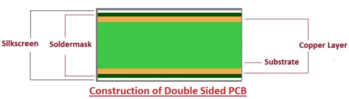
Single and Double-Layer PCB Stackup
Single and double-layer PCBs are commonly used in low-frequency analog designs operating below 10 kHz. However, these boards are prone to EMI issues due to larger signal loop areas. Here are key design tips to optimize their performance:
- Radial Routing for Power: Route power lines radially on the same layer to minimize the total length of the circuit, reducing inductance and EMI radiation.
- Ground Routing Proximity: Place ground traces close to critical signal traces to form a smaller loop area, reducing sensitivity to external interference and differential mode radiation.
- Double-Layer Ground Strategy: For double-layer PCBs, lay a wide ground trace on the opposite side of the signal trace, directly beneath it, to minimize the loop area and enhance EMI control.
By carefully managing routing and layout, you can significantly improve the electromagnetic compatibility of single and double-layer PCBs.
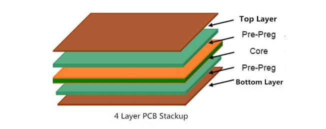
Four-Layer PCB Stackup Best Practices
Four-layer PCBs are widely used for their balance of performance and cost. Below are two common stackup configurations and their considerations:
SIG-GND(PWR)-PWR(GND)-SIG:
- Pros: Offers good signal integrity (SI) for boards with many chips.
- Cons: Large layer spacing in traditional 1.6 mm boards increases impedance control challenges and reduces board capacitance, impacting noise filtering.
- Use Case: Suitable for high-chip-density designs.
GND-SIG(PWR)-SIG(PWR)-GND:
- Pros: Provides excellent EMI control due to outer ground layers acting as shields. Ideal for low-chip-density designs with sufficient space around components.
- Cons: Slightly higher cost due to additional ground planes.
- Use Case: Preferred for applications prioritizing EMI performance.
Design Tips:
- Widen the spacing between the middle signal/power layers to reduce crosstalk.
- Ensure vertical routing directions between layers to minimize interference.
- Follow the 20H rule to control board edge radiation (keep power planes 20 times the dielectric thickness away from the board edge).
These configurations ensure a balance between signal integrity and EMI performance for 4-layer PCB stackups.
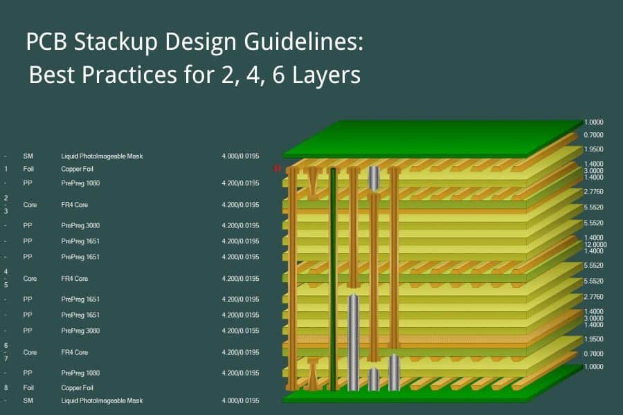
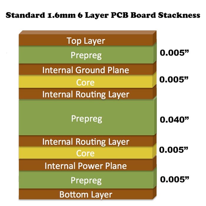
Six-Layer PCB Stackup for High-Density Designs
For designs with high chip density and high clock frequencies, a six-layer PCB stackup is recommended. Below are two effective configurations:
- SIG-GND-SIG-PWR-GND-SIG:
- Pros: Provides excellent signal integrity as each signal layer is adjacent to a ground plane. The power-ground pair enhances capacitance, and ground layers absorb magnetic lines of force effectively.
- Use Case: Ideal for high-speed digital designs requiring controlled impedance.
- GND-SIG-GND-PWR-SIG-GND:
- Pros: Offers superior EMI shielding due to complete ground planes on the top and bottom layers. Suitable for moderate-density designs.
- Cons: Higher manufacturing cost compared to the first option.
- Use Case: Best for applications where EMI control is critical.
Design Tips:
- Ensure impedance control by maintaining consistent layer spacing.
- Use ground planes to shield sensitive signals and reduce crosstalk.
- Simulate stackup designs using tools like Altium Designer or Cadence to verify performance.
A six-layer PCB stackup is ideal for complex designs requiring robust signal integrity and EMI performance.
Advanced Tips for PCB Stackup Optimization
To further enhance your PCB stackup design, consider these advanced strategies:
- Impedance Control: Use simulation tools to calculate trace widths and layer spacing for controlled impedance, ensuring signal integrity.
- Noise Filtering: Pair power and ground planes closely to maximize capacitance and filter high-frequency noise.
- Cost vs. Performance: Balance the number of layers with manufacturing costs. For example, a four-layer board may suffice for many applications, while six layers are reserved for high-performance designs.
- Simulation Tools: Leverage PCB design software like Altium Designer, Cadence, or KiCad to model stackups and predict EMI and SI performance.
These techniques help you fine-tune your PCB stackup for optimal performance.
Frequently Asked Questions (FAQ)
What is the best PCB stackup for EMI control?
The GND-SIG-SIG-GND configuration for four-layer PCBs and GND-SIG-GND-PWR-SIG-GND for six-layer PCBs offer superior EMI shielding due to their outer ground layers.
How do I choose between a 4-layer and 6-layer PCB?
Choose a 4-layer PCB for cost-sensitive designs with moderate complexity. Opt for a 6-layer PCB for high-density, high-speed designs requiring better signal integrity and EMI control.
How can I reduce EMI in PCB stackup design?
Minimize signal loop areas, use adjacent ground planes, and follow the 20H rule to reduce board edge radiation.
What tools are best for PCB stackup design?
Tools like Altium Designer, Cadence, and KiCad provide robust simulation and analysis for optimizing PCB stackups.
Conclusion
Effective PCB stackup design is essential for achieving reliable signal integrity, minimizing EMI, and optimizing manufacturing costs. By following the guidelines outlined above, you can design robust single, double, four, and six-layer PCBs tailored to your application’s needs.
Need professional PCB design services or further assistance? Contact our expert team at JHYPCB or explore our resources for more PCB design tips. Start optimizing your PCB stackup today!


