Table of Contents
Introduction
In today’s fast-paced electronics world, have you ever wondered what makes your smartphone’s processor run so smoothly, handling everything from quick app launches to seamless video streaming? It’s often the unsung hero behind the scenes: the IC substrate. This compact yet powerful component acts as the critical bridge between the tiny integrated circuit (IC) chip and the larger printed circuit board, ensuring reliable electrical connections, mechanical support, and efficient heat dissipation. Without it, modern devices simply couldn’t achieve the high performance and miniaturization we take for granted.
At its core, an IC substrate is a specialized type of circuit board designed specifically for mounting and interconnecting semiconductor chips. In PCB manufacturing, what is IC substrate often boils down to its role in enabling advanced packaging technologies—think of it as the intermediary that translates the microscopic world of chip-level operations into the macroscopic realm of everyday electronics. As industries push boundaries with trends like artificial intelligence (AI), 5G connectivity, and the Internet of Things (IoT), the demand for high-density, reliable IC substrates has skyrocketed. According to recent industry reports, the global semiconductor market is projected to grow by over 8% annually through 2030, with IC substrates playing a pivotal role in supporting this expansion by facilitating smaller, faster, and more energy-efficient designs.
In this comprehensive guide, we’ll dive deep into everything you need to know about IC substrates. We’ll start by defining what they are and how they differ from standard PCBs, then explore their various types, key functions and benefits, manufacturing processes, real-world applications, and even the challenges and innovations shaping their future. Whether you’re an engineer designing next-gen gadgets, a student curious about electronics, or a hobbyist tinkering with circuits, this article will equip you with the insights to understand—and appreciate—these essential components. Let’s get started.
What is an IC Substrate?
To truly grasp the role of IC substrates in today’s electronics, let’s break down what they are at a fundamental level. Imagine you’re holding a smartphone processor chip—tiny, intricate, and packed with billions of transistors. That chip can’t function in isolation; it needs a sturdy foundation to connect to the rest of the device. Enter the IC substrate: a specialized circuit board engineered specifically for mounting integrated circuits (ICs). In simple terms, an IC substrate is the intermediary platform that bridges the gap between the microscopic semiconductor chip and the larger PCB in your device. It provides essential electrical interconnections, mechanical support, and pathways for heat dissipation, ensuring the chip operates efficiently without overheating or signal loss.
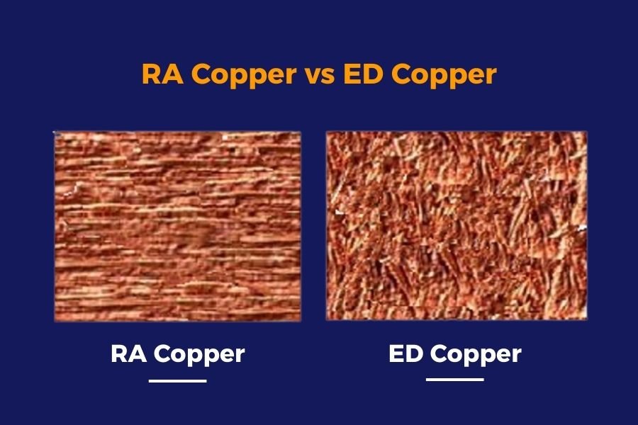
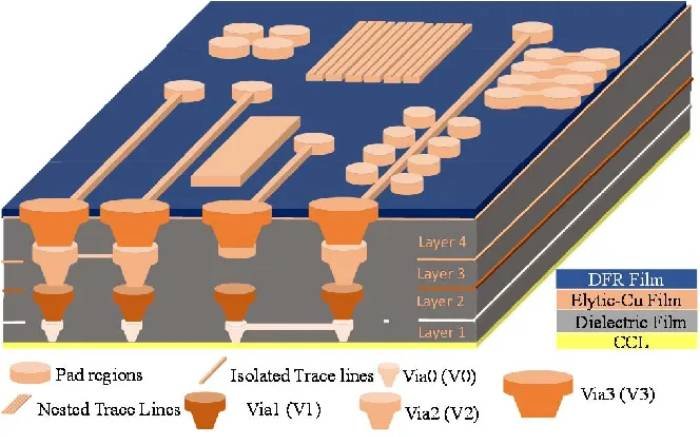
At a more technical level, the structure of an IC substrate resembles a miniaturized PCB but with far greater precision. It typically consists of a core layer made from materials like resin (such as BT or ABF) or ceramics (like aluminum oxide), sandwiched between conductive traces usually etched from copper foil. These traces form the wiring that carries signals and power. Tiny holes called vias—often laser-drilled to micron-level diameters—allow vertical connections between multiple layers, enabling high-density routing. On the surface, you’ll find contact pads or solder balls that interface directly with the chip on one side and the main PCB on the other. This layered design isn’t just about compactness; it’s optimized for handling the demands of high-speed data transmission and power distribution in modern tech.
One common question I hear is: how does an IC substrate differ from a standard PCB? While both serve as circuit platforms, the differences are stark and purposeful. A traditional PCB is like the highway system of an electronic device—broad, multi-layered, and designed to connect various components like resistors, capacitors, and even ICs themselves. In contrast, an IC substrate is more like a precision-engineered on-ramp, focused solely on packaging and supporting the IC chip. It’s much smaller (often just 10-50mm across and 0.1-1.5mm thick), with ultra-fine features: trace widths can dip below 10 microns, compared to PCBs where they’re typically in the tens or hundreds of microns. This high density comes at a cost—IC substrates are more expensive to produce due to advanced materials and manufacturing tolerances—but they deliver superior performance in areas like signal integrity and thermal management. For instance, where a PCB might handle general-purpose routing, an IC substrate minimizes electrical noise and crosstalk, making it indispensable for high-frequency applications.
What really sets IC substrates apart are their key characteristics that enable the miniaturization and efficiency we demand from gadgets today. First, there’s the push for extreme miniaturization: these substrates support chip-scale packaging, shrinking device footprints while packing in more functionality. High-density interconnects (HDI) allow thousands of connections in a tiny space, far beyond what a standard PCB can achieve. Thermal management is another standout feature—built-in vias and heat-spreading layers draw away excess heat from power-hungry chips, preventing throttling or failure in devices like laptops or servers. Finally, signal integrity ensures clean, fast data flow; low dielectric materials reduce signal loss, which is crucial for 5G networks or AI processors where even a microsecond delay matters. In essence, IC substrates aren’t just supportive—they’re the enablers of innovation, turning raw silicon into reliable, high-performing electronics. As we move into the next section, we’ll explore the different types of IC substrates and how their designs cater to specific needs.
Types of IC Substrates
Now that we’ve established the foundational role of IC substrates in bridging chips and PCBs, it’s time to unpack the variety available. Not all IC substrates are created equal—they’re tailored to meet diverse demands in terms of performance, size, and environment. Understanding the types helps you appreciate why one might be chosen for a high-power GPU in a gaming laptop versus a compact sensor in a wearable device. We’ll classify them into three main categories: by packaging method, by material characteristics, and by bonding technology. This breakdown draws from the wealth of designs that have evolved to support everything from everyday consumer tech to rugged industrial applications.
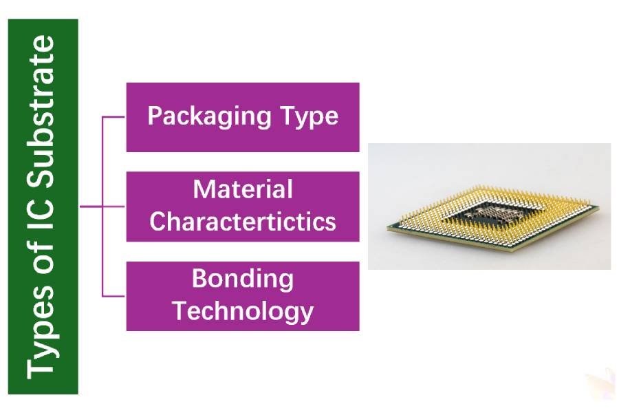
Classification by Packaging Method
This category focuses on how the substrate packages the semiconductor chip, influencing factors like pin density, thermal efficiency, and overall footprint. Each type addresses specific packaging needs, often driven by the chip’s complexity and the device’s requirements.
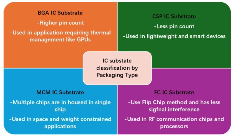
- Ball Grid Array (BGA) Substrates: These are among the most common for high-density applications. Instead of traditional pins, BGA uses a grid of solder balls on the underside to connect the chip to the substrate. This setup allows for hundreds or even thousands of connections in a small space, making it ideal for processors and memory modules where space is at a premium. Think of how BGA substrates excel in laptops or servers—they offer superior thermal performance by spreading heat across the array, reducing the risk of hotspots. However, they can be trickier to inspect and repair due to the hidden solder joints.
- Flip-Chip (FC) Substrates: Here, the chip is “flipped” upside down, with its active side facing the substrate and connected via solder bumps or balls. This direct attachment minimizes signal paths, leading to lower interference and faster data transfer. FC substrates shine in high-performance scenarios like GPUs, RF communication chips, or machine learning processors, where low latency and efficient heat dissipation are non-negotiable. The upside-down orientation also allows for better thermal management, but it demands precise alignment during assembly, which can increase manufacturing complexity.
- Chip Scale Package (CSP) Substrates: As the name suggests, these are designed for ultra-miniature packaging, where the substrate is nearly the same size as the chip itself—often just 1.2 times larger. CSP is perfect for low-pin-count applications, enabling slim profiles in consumer gadgets like smartphones, wearables, and IoT sensors. By reducing the mounting area, it supports the trend toward lighter, more portable devices, though it may not handle high-power loads as well as larger substrates.
- Multi-Chip Module (MCM) Substrates: For when one chip isn’t enough, MCM integrates multiple chips into a single package, each performing a unique function. This modular approach saves space and weight, making it suitable for constrained environments like aerospace or advanced computing systems. However, packing several chips together can amplify heat dissipation challenges, requiring careful design to avoid thermal bottlenecks.
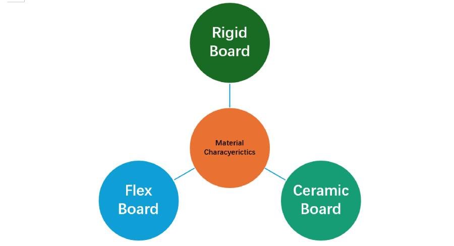
Classification by Material Characteristics
The material of an IC substrate dictates its durability, flexibility, and thermal properties, often chosen based on the operating environment. This classification ensures the substrate can withstand everything from everyday use to extreme conditions.
- Rigid Substrates: Built with sturdy materials like epoxy resin, Bismaleimide Triazine (BT), or Ajinomoto Build-up Film (ABF), these offer excellent stability and a low coefficient of thermal expansion (CTE) around 13-17 ppm/°C. They’re the go-to for traditional high-density boards, such as those in BGA packages, providing reliable performance in consumer electronics and automotive systems. Rigidity means they’re less prone to bending but might not suit flexible designs.
- Flexible Substrates: Made from polyimide (PI) or similar resins, these have a CTE of 13-27 ppm/°C and can bend without breaking, ideal for space-saving or wearable applications. They’re commonly used in foldable devices or medical implants, where conformity to shapes is key. The trade-off? They might not match the thermal conductivity of rigid options in high-heat scenarios.
- Ceramic Substrates: Composed of materials like aluminum oxide, aluminum nitride, or silicon carbide, these boast a very low CTE (6-8 ppm/°C) and exceptional reliability. They’re favored in harsh environments, such as military, aerospace, or medical devices, where high thermal conductivity and resistance to temperature extremes are crucial. Ceramics provide superior electrical insulation but can be more brittle and costly.
Classification by Bonding Technology
Bonding refers to how the chip attaches to the substrate, affecting assembly ease, performance, and cost. This category highlights the techniques that ensure secure, efficient connections.
- Wire Bonding: The simplest and most traditional method, where thin wires (gold, silver, copper, or aluminum) connect the chip’s pads to the substrate. It’s cost-effective and versatile for low-to-medium frequency applications, like basic consumer ICs. While reliable, it can introduce longer signal paths, potentially increasing latency in high-speed setups.
- Flip-Chip (FC) Bonding: As mentioned earlier, this uses solder bumps for direct connection, offering low signal interference and excellent thermal paths. It’s high-performance but requires advanced alignment tools during production.
- Tape Automated Bonding (TAB): Involving a pressure-sensitive adhesive on a flexible tape, this method bonds the chip to the substrate with conductive bumps. It’s great for thin, flexible packages in displays or sensors, providing automation efficiency, though it’s less common in ultra-high-density designs.
To make sense of these options at a glance, here’s a comparison table summarizing the key types across classifications:
| Type | Key Features | Applications | Pros | Cons |
|---|---|---|---|---|
| BGA (Packaging) | Solder ball grid, high pin density | Processors, memory modules | Excellent thermal performance | Difficult to inspect/repair |
| FC (Packaging/Bonding) | Direct bump connection, low interference | GPUs, RF chips | Fast signals, good heat dissipation | Assembly complexity |
| CSP (Packaging) | Near-chip size, low pins | Wearables, IoT sensors | Miniaturization, lightweight | Limited for high power |
| MCM (Packaging) | Multi-chip integration | Aerospace, computing | Space-saving | Heat management challenges |
| Rigid (Material) | Resin-based, stable CTE | Consumer electronics, automotive | Durable, cost-effective | Inflexible |
| Flexible (Material) | Polyimide, bendable | Foldables, medical implants | Conformable | Lower thermal conductivity |
| Ceramic (Material) | Low CTE, high conductivity | Military, aerospace | Reliable in extremes | Brittle, expensive |
| Wire Bonding (Bonding) | Wire connections, simple | Low-frequency ICs | Economical | Potential latency |
| TAB (Bonding) | Tape with bumps, automated | Displays, sensors | Efficient for flex | Less for high-density |
This variety ensures there’s an IC substrate suited to nearly any challenge, building directly on the core characteristics we discussed earlier—like high-density interconnects and thermal management. As we transition to the benefits and functions, you’ll see how these types translate into real-world advantages that drive innovation in electronics.
Key Functions and Benefits of IC Substrates
Having explored the diverse types of IC substrates, it’s clear they’re engineered for specific roles in the complex world of electronics. But what makes them so indispensable? In this section, we’ll dive into the key functions and benefits of IC substrates, illustrating how they empower modern devices to be smaller, faster, and more reliable. From enabling the sleek design of your smartwatch to ensuring a car’s navigation system performs flawlessly, IC substrates deliver critical advantages that shape the technology we rely on daily. Let’s break down their core functions and the tangible benefits they bring to the table, with real-world examples to bring it all to life.
Key Functions of IC Substrates
IC substrates are more than just a platform for chips—they’re multifunctional components that keep electronics running smoothly. Their primary roles include:
- Electrical Interconnection: At their heart, IC substrates act as a bridge, routing electrical signals between the chip’s microscopic circuits and the larger PCB. Think of them as the translator that ensures seamless communication, using conductive traces and vias to handle high-speed data and power distribution. Without this, your laptop’s processor couldn’t talk to its memory or other components.
- Mechanical Support: Chips are delicate, often just a few millimeters wide and prone to damage from stress or handling. The substrate provides a sturdy base, holding the chip securely in place and protecting it from physical shock or vibration during use or transport.
- Thermal Management: High-performance chips, like those in gaming consoles or AI servers, generate significant heat. IC substrates incorporate thermal vias and heat-spreading layers to channel this heat away, preventing performance throttling or failure. This is why your phone doesn’t overheat during a long video call.
- Environmental Protection: By encasing the chip, substrates shield it from moisture, dust, and oxidation. This is critical for devices used in harsh conditions, like automotive electronics exposed to humidity or industrial sensors in dusty factories.
- Miniaturization Enablement: Substrates support compact packaging, allowing chips to fit into tight spaces without sacrificing functionality. This is what makes ultra-thin smartphones or tiny medical implants possible.
Key Benefits of IC Substrates
These functions translate into powerful benefits that make IC substrates a cornerstone of modern electronics. Here’s how they add value, with examples to ground the concepts:
- Miniaturization for Compact Devices: IC substrates excel at shrinking device footprints while maintaining high functionality. Their high-density interconnects (HDI), enabled by laser-drilled micro-vias, allow thousands of connections in a space smaller than a postage stamp. For instance, in a smartwatch, a Chip Scale Package (CSP) substrate keeps the processor and sensors compact, enabling a sleek design you can wear comfortably all day. This benefit is crucial in consumer electronics, where users demand lightweight, portable devices without compromising power.
- Superior Thermal Management: Effective heat dissipation is non-negotiable in high-performance electronics. Substrates incorporate thermal vias and materials like ceramics or BT resin to draw heat away from chips. Take a gaming laptop: during intense gameplay, the GPU generates significant heat, but the substrate’s thermal design ensures it stays cool enough to maintain peak performance. This not only preserves the chip’s lifespan but also prevents lag or crashes, enhancing user experience.
- High-Density Interconnect Reliability: With advanced resin materials like Bismaleimide Triazine (BT) or Ajinomoto Build-up Film (ABF), IC substrates achieve stable impedance across layers, ensuring reliable signal transmission even under stress. They undergo rigorous testing, like thermal cycling and humidity resistance, to guarantee long-term durability. For example, in automotive applications like advanced driver-assistance systems (ADAS), substrates maintain consistent performance despite temperature swings or vibrations, ensuring safety-critical features like lane detection work flawlessly.
- Enhanced Electrical Performance: IC substrates are designed to minimize signal loss and crosstalk, critical for high-speed and high-frequency applications like 5G smartphones or AI processors. Low-dielectric-constant materials reduce signal distortion, while precise impedance control ensures clean data flow. Imagine streaming a 4K video on your phone: the substrate in the RF chip ensures the 5G signal remains strong and stable, delivering uninterrupted playback.
Real-World Example: Smartphones and Beyond
To illustrate, consider the smartphone in your pocket. Its processor, memory, and RF modules rely on IC substrates—often a mix of BGA for the main chip and CSP for smaller components. These substrates handle the rapid data exchange needed for multitasking, keep the chip cool during heavy apps like games, and fit everything into a slim device you can slip into your jeans. The result? A phone that’s powerful yet compact, with a battery life that lasts through your day. Beyond consumer electronics, substrates in medical devices like pacemakers ensure reliability in life-critical applications, using ceramic materials to withstand the body’s environment while keeping the device small enough for implantation.
These benefits build on the types we discussed earlier, where specific substrates—like flip-chip for high performance or flexible for wearables—cater to unique needs. The ability to deliver miniaturization, thermal efficiency, reliability, and electrical performance makes IC substrates indispensable across industries. In the next section, we’ll explore the intricate manufacturing process behind these tiny powerhouses, revealing the precision and innovation required to bring them to life.
IC Substrate Manufacturing Process
With a clear understanding of how IC substrates function and the benefits they bring, it’s time to pull back the curtain on how these intricate components are made. The manufacturing process of IC substrates is a marvel of precision engineering, blending advanced materials, cutting-edge technology, and meticulous quality control to create a platform that can handle the demands of modern electronics. Unlike standard PCBs, IC substrates require a higher degree of accuracy due to their microscopic features and high-density interconnects. In this section, we’ll walk through the key steps of the IC substrate manufacturing process, highlight the different fabrication methods, and touch on the challenges manufacturers face—all while keeping the explanation clear and engaging for anyone curious about how these tiny components come to life.
Key Steps in IC Substrate Manufacturing
The journey to create an IC substrate is a highly controlled, multi-step process that takes place in cleanroom environments to avoid even the tiniest speck of dust disrupting the delicate circuitry. Each step is designed to ensure precision, reliability, and performance, catering to the needs of high-speed, compact devices. Here’s a detailed look at the core stages:
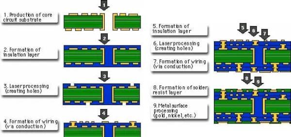
- Material Preparation and Layering
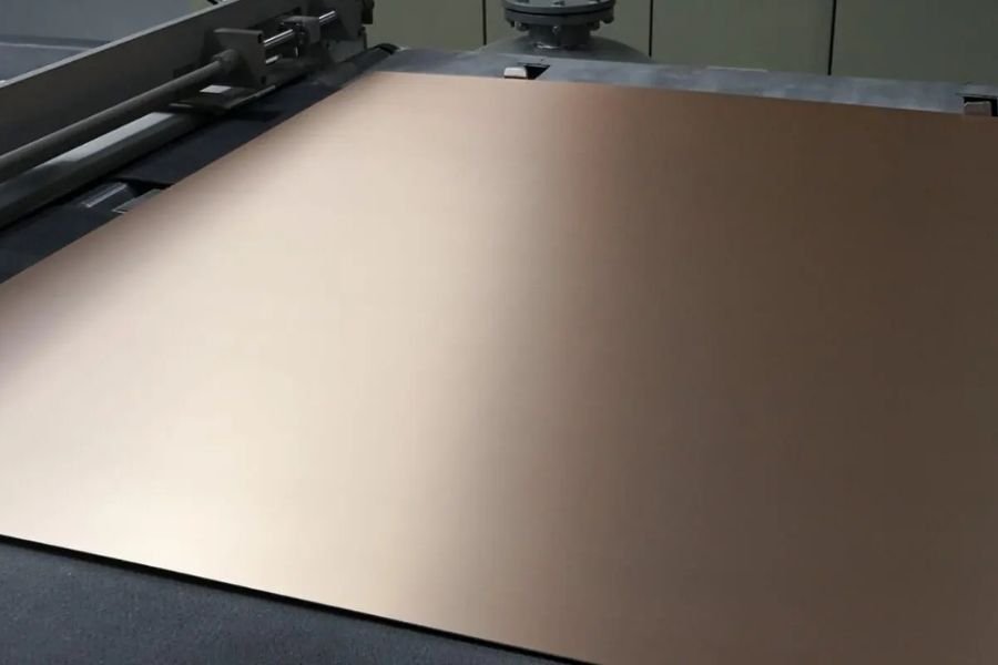
The process begins with selecting and preparing the core material, typically a thin dielectric like FR-4, Bismaleimide Triazine (BT) resin, or Ajinomoto Build-up Film (ABF). These materials are chosen for their electrical insulation, thermal stability, and mechanical strength. Copper foil is laminated onto both sides of the core, forming the foundation for conductive paths. The layering process involves stacking multiple thin laminates, often under high pressure and temperature, to create a solid, multi-layered structure. This step is critical, as even a slight misalignment can compromise the substrate’s performance. - Drilling and Via Formation
To connect the layers electrically, tiny holes called vias are drilled into the substrate. Unlike traditional PCBs, where mechanical drilling might suffice, IC substrates rely heavily on laser drilling to create micro-vias with diameters as small as 10-50 microns. These micro-vias enable high-density interconnects, allowing signals to pass between layers efficiently. After drilling, a cleaning process (desmearing) removes debris to ensure smooth, reliable connections. Precision here is paramount—any deviation in via placement can disrupt signal integrity. - Circuit Patterning and Etching
Next, the substrate’s circuitry is defined through photolithography. A photosensitive film (photoresist) is applied to the copper surface, and ultraviolet light is used to expose the desired circuit pattern. Unwanted copper is then etched away using chemical or plasma processes, leaving behind precise conductive traces. These traces can be as narrow as 10 microns, far finer than those on standard PCBs. This step requires exceptional accuracy to avoid defects like incomplete etching, which could cause short circuits or signal loss. - Plating
To make the vias conductive, they’re plated with copper, creating vertical pathways that link the substrate’s layers. This electroplating process ensures robust electrical connections across the multi-layered structure. Additional copper may be deposited to strengthen critical areas, enhancing the substrate’s durability and conductivity. - Solder Mask Application
A protective solder mask is applied to the substrate’s surface to shield the circuitry from environmental damage like moisture or oxidation. The mask covers all but the areas intended for soldering, such as pads or solder balls, preventing short circuits during assembly. This step also enhances the substrate’s longevity, especially in harsh conditions like automotive or industrial settings. - Surface Finishing
To improve solderability and protect exposed copper pads from oxidation, a surface finish is applied. Common finishes include Electroless Nickel Immersion Gold (ENIG), Organic Solderability Preservative (OSP), or Immersion Tin. These coatings ensure reliable connections when the chip is mounted and maintain performance over time. Uniform thickness is critical to avoid weak solder joints. - Inspection and Testing
The final step involves rigorous quality checks to ensure the substrate meets strict electrical, functional, and visual standards. Automated optical inspection (AOI), X-ray imaging, and electrical testing detect defects like voids, misaligned vias, or incomplete circuits. Only substrates passing these tests move on to chip assembly, ensuring reliability in applications from smartphones to medical devices.
Fabrication Methods
IC substrates are manufactured using three primary methods, each balancing precision, cost, and complexity. These methods, rooted in PCB manufacturing but refined for substrates, determine how the circuitry is formed:
- Subtractive Process (SP): This traditional method starts with a copper-clad core, covered with a photoresist mask. Unwanted copper is etched away chemically to reveal the circuit pattern. While cost-effective, it’s less precise due to lateral etching, limiting trace widths to around 50 microns. It’s suitable for simpler substrates but struggles with ultra-fine features.
- Additive Process (AP): Here, copper is selectively deposited onto the core where circuits are needed, using a photosensitive catalyst and chemical plating. This method avoids lateral etching, achieving finer traces (down to 10 microns) and higher resolution. It’s ideal for high-density substrates but requires more sophisticated equipment, increasing costs.
- Modified Semi-Additive Process (MSAP): A hybrid approach, MSAP starts with a thin copper seed layer, applies a photoresist, and deposits additional copper to form circuits. A final flash etch refines the pattern. MSAP combines the precision of additive methods with cost efficiencies, making it popular for advanced substrates like those in 5G or AI applications.
Manufacturing Challenges
Creating IC substrates is no easy feat—each step pushes the limits of technology and precision. Key challenges include:
- Precision Demands: Micro-vias and fine traces require sub-micron accuracy. Misaligned vias or uneven etching can lead to signal failures. Advanced tools like laser direct imaging (LDI) are now standard to meet these tolerances.
- Material Innovation: As devices shrink, substrates need thinner, more thermally efficient materials like advanced BT or ABF resins. Developing these without compromising strength or cost is a constant hurdle.
- Defect Detection: Voids or micro-cracks in multi-layered substrates can degrade performance. High-resolution X-ray and AOI systems are critical but add complexity and cost to production.
- Cost Control: The intricate processes and materials (e.g., ceramics or polyimide) drive up costs. Balancing performance with affordability is a persistent challenge, especially for consumer electronics where margins are tight.
These steps and challenges build on the benefits we discussed earlier, like high-density interconnects and thermal management, by showing the engineering feats required to achieve them. For example, the precision in laser drilling directly enables the miniaturization that makes modern wearables possible. As we move to the next section, we’ll explore how these carefully crafted substrates are applied across industries, from smartphones to life-saving medical devices, bringing their benefits to life in the real world.
Applications of IC Substrates
With the intricate manufacturing process of IC substrates now clear, it’s time to see where these tiny powerhouses shine in the real world. IC substrates are the unsung heroes behind the electronics that power our daily lives, from the smartphones we can’t put down to the advanced systems keeping cars and medical devices running smoothly. Their ability to support high-density connections, manage heat, and ensure reliability makes them indispensable across a wide range of industries.
Applications of IC Substrates
IC substrates are versatile, enabling everything from consumer gadgets to mission-critical systems. Their compact size, high-density interconnects, and robust thermal management make them ideal for applications requiring speed, reliability, and miniaturization. Below, we dive into the primary industries where IC substrates play a pivotal role, illustrating their impact with specific use cases.
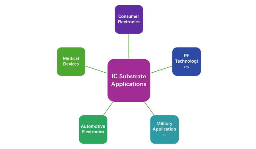
- Consumer Electronics
IC substrates are the backbone of devices like smartphones, tablets, and laptops, where space is tight and performance expectations are sky-high. Technologies like System-in-Package (SiP) and Package-on-Package (PoP) rely on substrates to integrate multiple chips or components into a single compact module. For example, in a modern smartphone, a BGA or CSP substrate supports the main processor and memory chips, enabling seamless multitasking and fast app performance while keeping the device slim. These substrates use high-density interconnects to pack thousands of connections into a small footprint, ensuring your phone can stream 4K videos or run AI-driven features like voice recognition without lag. The consumer electronics market, projected to grow at a CAGR of 7.5% through 2030, leans heavily on IC substrates to meet demands for smaller, smarter devices. - Automotive and Mobility
The automotive industry is undergoing a transformation with the rise of electric vehicles (EVs), autonomous driving, and 5G connectivity. IC substrates are critical for advanced driver-assistance systems (ADAS), infotainment, and navigation modules. They must withstand harsh conditions like temperature swings and vibrations, making rigid or ceramic substrates a popular choice. For instance, in an ADAS system, a flip-chip substrate ensures the processor handling real-time data from cameras and sensors operates reliably, enabling features like lane-keeping or collision avoidance. Substrates also support high-performance computing (HPC) for autonomous vehicles, where low-latency signal transmission is vital. The automotive electronics market, expected to reach $400 billion by 2030, relies on IC substrates for safety and performance. - Medical Devices
In healthcare, IC substrates enable life-saving technologies in compact, reliable packages. Devices like pacemakers, neurostimulators, and diagnostic sensors use substrates to integrate tiny chips with ultra-thin laminates and biocompatible surface finishes. A ceramic substrate, for example, might be used in a pacemaker to ensure durability and reliability in the body’s challenging environment. These substrates must pass stringent tests for biocompatibility and long-term stability, as even a minor failure could be critical. By enabling miniaturization, IC substrates allow medical implants to be less invasive, improving patient comfort and outcomes. The medical electronics sector is growing rapidly, driven by demand for wearable health monitors and smart diagnostics. - Industrial Applications
Industrial equipment, from robotics to intelligent sensors, relies on IC substrates for durability in harsh environments. Vision systems in automated manufacturing lines, for example, use substrates to support high-speed processors that analyze real-time data for quality control. These substrates, often rigid or ceramic, are designed to withstand long service cycles, high temperatures, and exposure to dust or chemicals. A multi-chip module (MCM) substrate might integrate sensors and processors in a single package, reducing space and improving efficiency in a factory setting. As Industry 4.0 drives automation, IC substrates are key to enabling smart, connected systems. - Telecommunications and RF Technologies
The rollout of 5G and the expansion of IoT have spiked demand for IC substrates in RF modules and high-speed communication devices. Substrates with low dielectric loss, like those made with BT resin, ensure signal integrity for high-frequency applications. For example, in a 5G base station, a flip-chip substrate supports the RF chip, minimizing signal loss to deliver fast, reliable connectivity. These substrates are critical for maintaining performance in dense urban networks or IoT ecosystems, where billions of devices need seamless data exchange. - Military and Aerospace
In demanding fields like military and aerospace, IC substrates must deliver unmatched reliability under extreme conditions. Ceramic substrates, with their low CTE and high thermal conductivity, are often used in avionics, satellites, or defense electronics like radar systems. For instance, a substrate in a drone’s navigation system ensures the chip can handle rapid data processing in high-altitude, low-temperature environments. These applications prioritize durability and performance, making substrates a critical component in mission-critical systems.
Industry Trends
The applications above are fueled by broader trends in the semiconductor industry. According to recent data, the global semiconductor market is expected to grow at a CAGR of 8.6% through 2030, driven by demand for AI, IoT, and 5G. IC substrates are evolving to support these trends, with innovations like high-density interconnect (HDI) substrates and through-silicon vias (TSVs) enabling 3D chip stacking for greater performance in smaller spaces. Sustainability is also gaining traction, with manufacturers exploring halogen-free and recyclable materials to reduce environmental impact. Heterogeneous integration—combining multiple chip types on a single substrate—is another growth area, particularly for advanced computing and automotive applications.
Real-World Example: Automotive ADAS
To bring this to life, consider a modern car equipped with an ADAS system. The system relies on a flip-chip BGA substrate to support its main processor, which handles data from cameras, radar, and lidar sensors. The substrate’s high-density interconnects ensure real-time processing for features like adaptive cruise control, while its thermal vias keep the chip cool during long drives. Rigorous testing for thermal cycling and vibration resistance guarantees reliability, even on bumpy roads or in extreme weather. This single substrate enables a safer, smarter driving experience, showcasing how IC substrates translate technical prowess into practical impact.
These applications build on the manufacturing precision and benefits we’ve discussed, like miniaturization and thermal management, showing how substrates enable cutting-edge technology across industries. In the next section, we’ll tackle the challenges and innovations in IC substrate design, exploring how manufacturers push boundaries to meet the demands of an ever-evolving electronics landscape.
Challenges and Innovations in IC Substrates
After seeing how IC substrates power everything from smartphones to self-driving cars, it’s clear they’re critical to modern electronics. But creating and improving these tiny, complex components isn’t without hurdles. The push for smaller, faster, and more efficient devices brings a host of challenges, from managing heat in densely packed circuits to controlling costs in a competitive market. At the same time, relentless innovation is addressing these obstacles, paving the way for next-generation substrates that support emerging technologies like AI and 5G.
Challenges in IC Substrate Design and Manufacturing
The relentless drive for miniaturization and performance in electronics puts immense pressure on IC substrate production. Each challenge stems from the need to balance precision, reliability, and cost in increasingly demanding applications. Here are the primary hurdles manufacturers face:
- Miniaturization-Induced Thermal Issues: As devices shrink and chips become more powerful, heat dissipation becomes a major concern. High-density interconnects (HDI) and tightly packed components generate significant heat in a confined space, risking performance degradation or chip failure. For example, in a 5G smartphone processor, the substrate must manage heat from billions of transistors operating at high frequencies, all within a footprint smaller than a coin. Poor thermal design can lead to throttling, as seen when devices slow down during heavy tasks like gaming.
- Cost Pressures: IC substrates require advanced materials (e.g., BT resin, ceramics) and precision processes like laser drilling or photolithography, driving up production costs. This is especially challenging in consumer electronics, where slim profit margins demand affordability without sacrificing quality. For instance, producing a high-density substrate for a budget smartphone involves balancing expensive HDI techniques with cost-effective manufacturing methods, a delicate dance for manufacturers.
- Defect Detection and Quality Control: The microscopic features of IC substrates—traces as thin as 10 microns, vias under 50 microns—make defects like voids, cracks, or incomplete plating hard to detect. A single void in a thermal via can disrupt heat flow, while a misaligned trace can cause signal loss. Advanced inspection tools like X-ray imaging or automated optical inspection (AOI) are essential but add time and cost. In high-reliability applications like medical implants, even a 0.01% defect rate is unacceptable.
- Material and Process Complexity: Achieving the fine features needed for modern substrates requires cutting-edge materials and techniques. For example, thinner dielectric layers (sometimes under 50 microns) are needed for 5G or AI applications, but these materials must maintain mechanical strength and low dielectric loss. Similarly, processes like modified semi-additive (MSAP) demand precise control to avoid defects, increasing the complexity of production lines.
- Scalability for Emerging Applications: As industries like IoT and autonomous vehicles grow, substrates must scale to meet diverse needs—high power for servers, ultra-thin for wearables, or rugged for aerospace. Each application demands tailored designs, materials, and testing, stretching manufacturing capabilities. For instance, a substrate for an IoT sensor must be low-cost and compact, while one for a satellite requires extreme durability, creating a wide range of technical demands.
Innovations Addressing These Challenges
To tackle these hurdles, the IC substrate industry is pushing boundaries with innovative technologies and approaches. These advancements not only solve current problems but also enable the next wave of electronics. Here’s a look at the key innovations:
- Through-Silicon Vias (TSVs) for 3D Stacking: TSVs are vertical connections that pass through the silicon chip itself, integrated into the substrate to enable 3D chip stacking. This allows multiple chips to be stacked vertically, reducing footprint and improving performance. For example, in high-performance computing (HPC) for AI, TSV-enabled substrates cut signal latency by shortening interconnect lengths, while also improving thermal management by distributing heat across layers. This technology is critical for advanced packaging like chiplet designs, where multiple small chips work together in one package.
- Embedded Passive Components: To save space and enhance performance, manufacturers are embedding passive components like resistors and capacitors directly into the substrate. This reduces the need for external components, shrinking the overall package size and improving signal integrity. In a wearable fitness tracker, for instance, an embedded capacitor in the substrate can stabilize power delivery to the sensor chip, enabling a slimmer design without sacrificing reliability.
- High-Density Interconnect (HDI) Advancements: HDI technology continues to evolve, with finer trace widths (down to 5 microns) and smaller micro-vias enabled by advanced laser drilling and MSAP processes. These improvements support the ultra-dense connections needed for 5G RF modules or AI processors. For example, a modern GPU substrate might use HDI to pack thousands of connections into a 20mm square, ensuring fast data transfer without signal crosstalk.
- Advanced Materials: New materials like low-loss dielectrics and high-thermal-conductivity resins are addressing thermal and electrical challenges. For instance, next-generation BT resins with lower dielectric constants reduce signal loss in high-frequency 5G applications, while ceramic substrates with thermal conductivities above 150 W/m·K improve heat dissipation in aerospace systems. These materials enable substrates to handle higher power densities without compromising reliability.
- Automation and AI in Manufacturing: To improve defect detection and reduce costs, manufacturers are adopting AI-driven inspection systems and automated production lines. AI can analyze X-ray images to spot micro-cracks invisible to the human eye, while robotic automation ensures consistent laser drilling and plating. This not only boosts yield rates but also lowers costs, making high-quality substrates more accessible for consumer devices.
Future Trends in IC Substrate Technology
Looking ahead, the IC substrate industry is poised for transformative growth, driven by emerging technologies and sustainability demands. Key trends include:
- Sustainable Materials: With environmental concerns rising, manufacturers are exploring halogen-free resins and recyclable substrates to reduce ecological impact. For example, bio-based dielectrics are being tested to replace traditional materials, aligning with global sustainability goals without sacrificing performance.
- Heterogeneous Integration: This approach combines different chip types (e.g., logic, memory, and RF) on a single substrate, optimizing performance for applications like autonomous vehicles. Heterogeneous integration relies on advanced substrates with TSVs and embedded components, enabling compact, high-efficiency systems.
- Wafer-Level Packaging (WLP): WLP integrates substrate manufacturing directly onto the silicon wafer, streamlining production and reducing costs. This is gaining traction in consumer electronics, where WLP substrates enable ultra-thin packages for devices like smartwatches or earbuds.
- Support for AI and 5G: As AI and 5G networks expand, substrates are being designed for higher frequencies (up to 100 GHz) and greater power efficiency. Innovations like ultra-low-loss dielectrics and advanced thermal vias will support the next generation of AI servers and 5G infrastructure.
These innovations build on the applications we discussed, like 5G telecommunications and automotive ADAS, by enabling substrates to meet the growing demands of speed, reliability, and compactness. For example, TSVs and HDI advancements make it possible to create the ultra-dense substrates powering AI-driven data centers. As we move to the next section, we’ll explore the design considerations engineers must navigate to bring these innovations to life, ensuring substrates meet the specific needs of each application.
Design Considerations for IC Substrates
Designing an IC substrate is a balancing act, requiring engineers to juggle electrical performance, thermal management, mechanical stability, and manufacturability—all while keeping costs in check. Each decision impacts the substrate’s ability to support the chip and perform reliably in its intended application, whether it’s powering a 5G smartphone or a medical implant. Below, we outline the critical factors engineers must consider, along with practical tips to optimize designs for real-world success.
Material Selection
The choice of substrate material sets the foundation for performance, influencing electrical, thermal, and mechanical properties. Key considerations include:
- Dielectric Properties: Low-dielectric-constant materials, like Bismaleimide Triazine (BT) or Ajinomoto Build-up Film (ABF), minimize signal loss in high-frequency applications like 5G RF modules. For example, a dielectric constant below 3.5 ensures clean signal transmission for a smartphone’s processor handling fast data streams.
- Thermal Conductivity: Materials like ceramics (e.g., aluminum nitride with 150 W/m·K) or advanced resins excel in dissipating heat, critical for high-power chips in AI servers. Engineers must match the material’s thermal conductivity to the chip’s heat output to prevent throttling.
- Coefficient of Thermal Expansion (CTE): The substrate’s CTE should align closely with the chip (typically 3-7 ppm/°C for silicon) to avoid stress during temperature changes. For instance, ceramic substrates (6-8 ppm/°C) are ideal for aerospace applications, while BT resins (13-17 ppm/°C) suit consumer electronics.
- Mechanical Strength: Rigid materials like FR-4 or BT provide stability for BGA substrates in laptops, while flexible polyimide is chosen for bendable wearables. Engineers must ensure the material withstands mechanical stress, like vibrations in automotive systems.
Tip: Use simulation tools to model CTE mismatches and thermal performance before finalizing material choices. For cost-sensitive projects, balance high-performance materials with affordable options like modified FR-4 for less demanding applications.
Thermal Management
Effective heat dissipation is critical, as modern chips generate significant heat in compact spaces. Poor thermal design can lead to performance drops or premature failure. Key considerations include:
- Thermal Vias: Incorporate arrays of micro-vias filled with copper to channel heat from the chip to a heat spreader or PCB. For example, in a gaming GPU, thermal vias can reduce chip temperature by 10-15°C, maintaining performance during intense sessions.
- Heat-Spreading Layers: Integrate copper planes or metal core layers to distribute heat evenly across the substrate. In a 5G base station, this ensures the RF chip doesn’t overheat under constant high-frequency operation.
- Material Selection for Heat: Choose high-thermal-conductivity materials like ceramics for high-power applications or resins with thermal fillers for cost-effective solutions. For instance, a ceramic substrate in a medical pacemaker ensures reliable heat dissipation in a confined space.
Tip: Use thermal simulation software to optimize via placement and size. Ensure vias are placed directly under high-heat areas of the chip, and verify heat flow paths to avoid bottlenecks.
Signal Integrity
Maintaining clean, fast signal transmission is paramount, especially for high-speed applications like AI processors or 5G devices. Key considerations include:
- Impedance Control: Design traces and vias to maintain consistent impedance (typically 50 ohms for high-speed signals). For example, in an AI server, precise impedance matching prevents signal reflections that could disrupt data processing.
- Low Dielectric Loss: Select materials with low loss tangents (e.g., below 0.005) to minimize signal attenuation. In RF modules, this ensures clear 5G signals over long distances.
- Trace Geometry: Keep trace widths and spacing uniform to avoid crosstalk. For high-density interconnects (HDI), traces as narrow as 5-10 microns are common, requiring precise photolithography to maintain signal integrity.
Tip: Use electromagnetic simulation tools to model signal paths and identify potential crosstalk. Minimize trace lengths and avoid sharp bends to reduce signal distortion.
Reliability and Durability
IC substrates must withstand environmental stresses, from temperature swings to humidity, especially in automotive or medical applications. Key considerations include:
- Thermal Cycling Resistance: Design substrates to endure repeated heating and cooling, as in automotive ADAS systems exposed to -40°C to 85°C. Materials with low CTE and robust solder joints prevent cracking or delamination.
- Moisture Resistance: Apply high-quality solder masks and surface finishes like ENIG to protect against humidity, critical for substrates in wearable health monitors exposed to sweat or rain.
- Mechanical Robustness: Ensure the substrate can handle vibrations or shocks, as in industrial sensors. Rigid substrates or reinforced cores provide the necessary strength.
Tip: Conduct accelerated life testing, like Highly Accelerated Stress Testing (HAST), to simulate years of environmental exposure. Verify solder joint integrity under thermal and mechanical stress.
Manufacturability and Cost
A great design is only as good as its ability to be produced reliably and affordably. Key considerations include:
- Process Compatibility: Ensure the design aligns with manufacturing capabilities, like laser drilling for micro-vias or MSAP for fine traces. Overly complex designs can increase defect rates, as seen when pushing trace widths below 5 microns without advanced equipment.
- Cost Optimization: Balance high-performance features with cost. For example, use additive processes for ultra-fine traces in high-end substrates, but opt for subtractive processes for cost-sensitive consumer devices.
- Yield Improvement: Design with tolerances that account for manufacturing variations. For instance, slightly wider vias (e.g., 50 microns vs. 30 microns) can improve yield without sacrificing performance in less demanding applications.
Tip: Collaborate with manufacturers early in the design phase to align specifications with production capabilities. Use design-for-manufacturability (DFM) guidelines to minimize defects and reduce costs.
Practical Example: Designing for a 5G Smartphone
Consider designing a substrate for a 5G smartphone’s RF chip. Engineers might choose a BT resin substrate for its low dielectric loss (ensuring clear 5G signals) and a CTE of 13 ppm/°C to match the chip. Thermal vias are placed under the chip to dissipate heat from high-frequency operations, while HDI traces (10 microns wide) maintain signal integrity. A robust ENIG finish protects against humidity, and the design uses MSAP to achieve fine features cost-effectively. Simulations confirm impedance control and thermal performance, ensuring the substrate supports fast, reliable connectivity in a compact package.
These design considerations build on the innovations discussed earlier, like TSVs and HDI, by showing how they’re applied practically to meet specific application needs. They also tie back to the applications in Section 6, ensuring substrates deliver the performance required for smartphones, automotive systems, or medical devices. In the next section, we’ll wrap up with a conclusion that ties all these insights together, highlighting the critical role of IC substrates in modern electronics.
Conclusion
IC substrates may be small, but their impact on modern electronics is monumental. As we’ve explored in this guide, these specialized circuit boards are the critical bridge between semiconductor chips and the larger PCBs in devices we use every day. They enable the miniaturization that makes sleek smartphones and wearables possible, ensure reliable performance in high-speed applications like 5G and AI, and withstand the harsh conditions of automotive and aerospace systems. By providing electrical interconnections, mechanical support, and advanced thermal management, IC substrates are the unsung heroes behind the technology shaping our world.
Let’s recap the journey. We started by defining the IC substrate as a high-precision platform that connects chips to PCBs, distinguished from standard PCBs by its ultra-fine features and high-density interconnects. We explored the various types—BGA, flip-chip, CSP, and MCM, along with rigid, flexible, and ceramic materials—each tailored to specific needs like power efficiency or durability. The key functions and benefits, like enabling compact designs and ensuring signal integrity, showed why substrates are indispensable in consumer electronics, automotive, medical, and industrial applications. We delved into the intricate manufacturing process, from laser-drilled micro-vias to rigorous testing, highlighting the precision required to achieve these benefits. We also tackled the challenges, like thermal management and cost control, and showcased innovations like through-silicon vias (TSVs) and embedded components that are pushing the industry forward. Finally, we covered design considerations, offering practical tips for engineers to optimize substrates for performance and reliability.
As the semiconductor industry continues to grow—projected to reach a market size of over $1 trillion by 2030—IC substrates will remain at the forefront, supporting trends like AI, IoT, and sustainable electronics. Their ability to evolve with these demands ensures they’ll continue to power the next generation of devices, from smarter cars to life-saving medical implants.
Common Questions About IC Substrates
To wrap up, let’s address some frequently asked questions to deepen your understanding and spark curiosity:
- What is the difference between an IC substrate and a PCB?
While both are circuit platforms, IC substrates are smaller, with finer traces (often below 10 microns) and higher density for chip-level packaging. PCBs are larger, handling broader component connections. Substrates prioritize signal integrity and thermal management for high-performance chips, making them more specialized and costly. - Why are IC substrates so critical for 5G technology?
5G devices require high-frequency signals (up to 100 GHz) with minimal loss. IC substrates, with low-dielectric materials and precise impedance control, ensure clean signal transmission and manage heat from high-speed chips, enabling reliable connectivity in smartphones and base stations. - How do IC substrates contribute to miniaturization?
Through high-density interconnects (HDI) and technologies like CSP or TSVs, substrates pack thousands of connections into tiny spaces. This allows devices like smartwatches to remain slim while delivering powerful performance.
For those looking to bring their electronics projects to life with high-quality IC substrate solutions, JHYPCB offers comprehensive PCB manufacturing and assembly services, from prototypes to multilayer boards. Contact us at sales@pcbjhy.com to explore how we can support your needs with precision and expertise.