Table of Contents
In today’s fast-paced world, electronic devices are everywhere—from smartphones and laptops to smart home appliances and industrial machinery. As demand for reliable, high-performance electronics continues to grow, understanding the core components behind these devices becomes increasingly important. At the heart of every electronic gadget lies a printed circuit board, and one of its most critical elements is copper foil. This thin, versatile material serves as the backbone for seamless electrical flow and connectivity. In this guide, we’ll explore the role of copper foil in PCB manufacturing, drawing on industry insights to explain why it’s indispensable for modern electronics.
Whether you’re an engineer, hobbyist, or simply curious about how gadgets work, this post will break down the fundamentals step by step, highlighting copper foil’s properties, integration, and benefits in PCB production.
What Is a PCB and Why Does It Matter?
To appreciate copper foil’s role, it’s helpful to start with the basics of PCBs. A PCB is a non-conductive substrate—typically made from materials like fiberglass (FR4) or plastic—that supports and electrically connects various components. These boards feature conductive pathways, known as traces or tracks, which enable signals to flow between elements such as resistors, capacitors, and integrated circuits.
PCBs are essential in virtually all electronic products, ensuring reliable operation. The quality of materials like copper foil directly influences performance, durability, and signal integrity, making it a key factor in the manufacturing process.
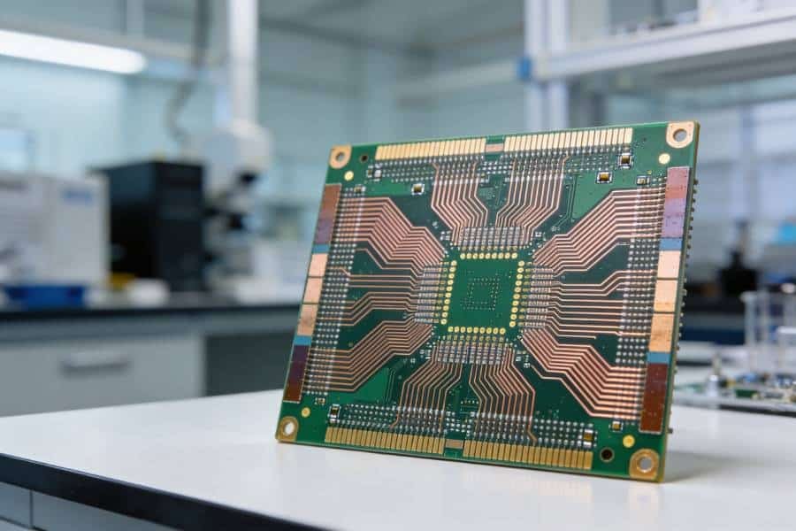
The Fundamentals of Copper Foil in PCBs
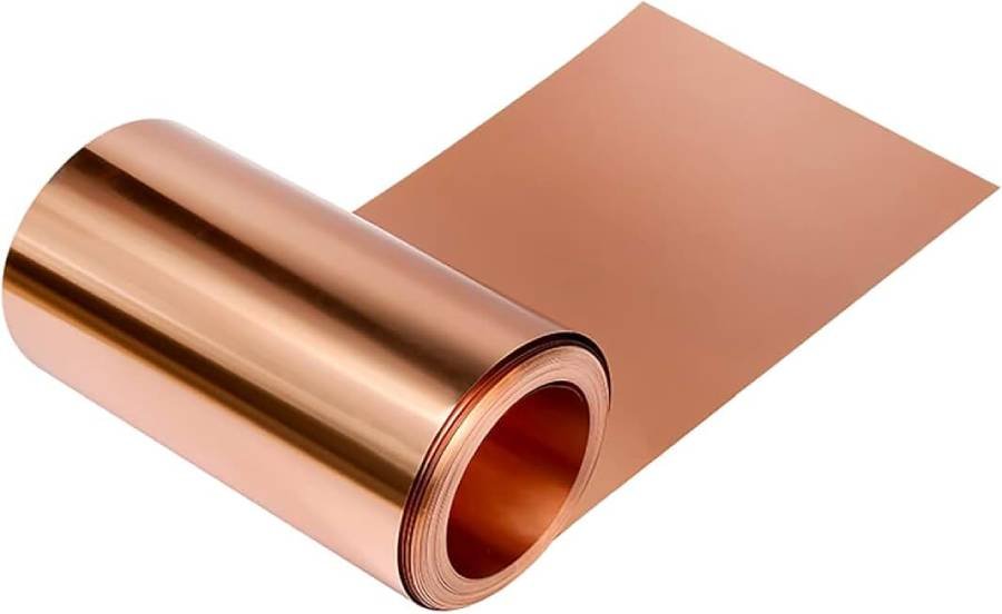
Copper foil is a thin sheet of copper laminated onto the PCB substrate. It’s often measured in ounces per square foot (oz/ft²), with thicknesses commonly ranging from 0.5 oz to 2 oz or more, depending on the application’s needs. What makes copper the preferred choice? Its standout properties include:
- High Electrical Conductivity: Copper has excellent conductivity due to its free electrons, which move with low resistance. This allows efficient transmission of electrical charges, minimizing signal loss or interference—vital for high-speed circuits in computers or telecom equipment.
- Excellent Thermal Management: Copper dissipates heat effectively, helping prevent overheating in compact, high-power devices.
- Strong Adhesion and Durability: It bonds well with insulating layers and substrates. After lamination, etching removes excess copper to create precise patterns of traces, pads, and vias.
Essentially, copper foil functions like the “veins” of the PCB, directing power and signals across the board. Without these conductive paths, components couldn’t interact, rendering the device non-functional.
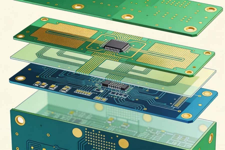
How Copper Foil Is Integrated into PCB Manufacturing
Copper foil integration occurs early in the fabrication process. Here’s a simplified overview:
- Substrate Preparation: Begin with a non-conductive base, such as epoxy resin reinforced with glass fibers.
- Lamination: Apply copper foil to one or both sides under heat and pressure. For multilayer boards, stack multiple copper-clad layers and bond them.
- Etching and Patterning: Use photoresist and chemical etchants to remove unwanted copper, forming the circuit layout. Precision here is crucial to avoid shorts or opens.
- Additional Layers and Finishing: Add solder mask, silkscreen, and surface finishes (e.g., HASL, ENIG, or OSP) to protect the copper and improve solderability.
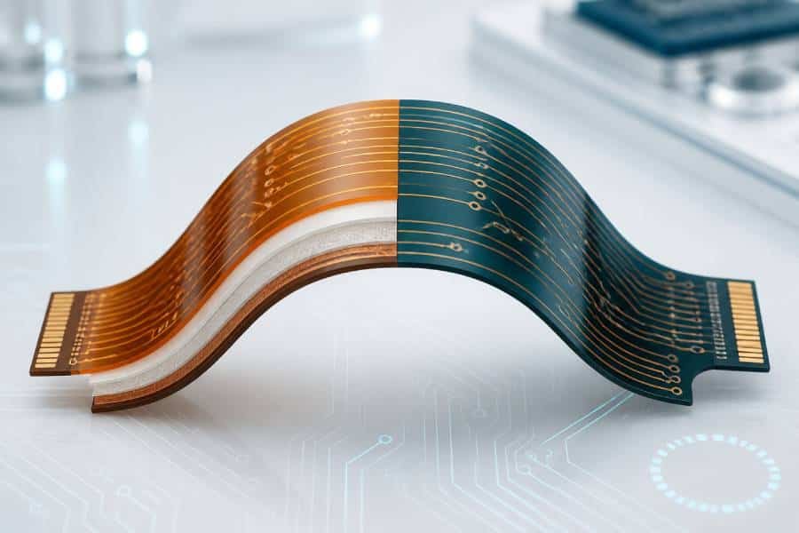
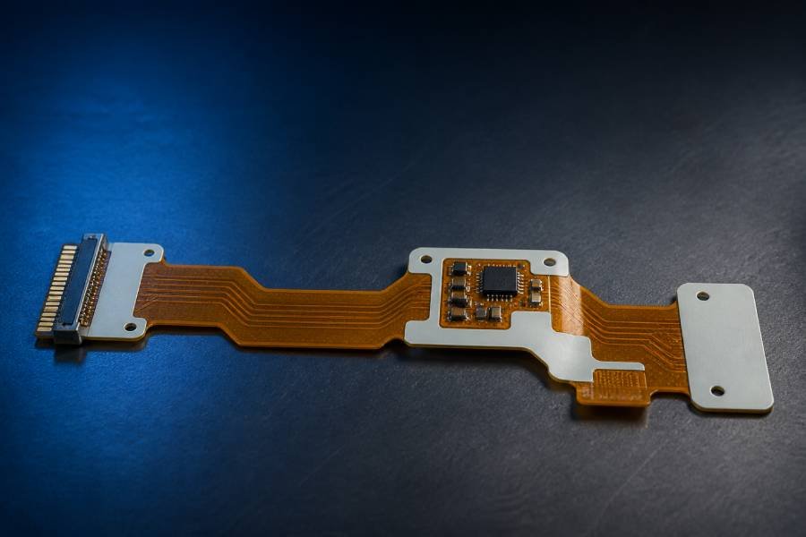
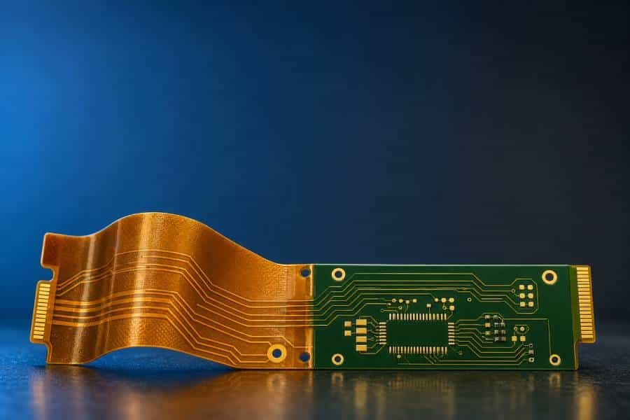
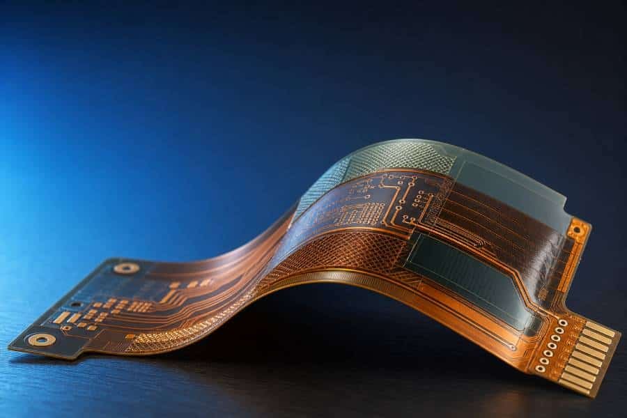
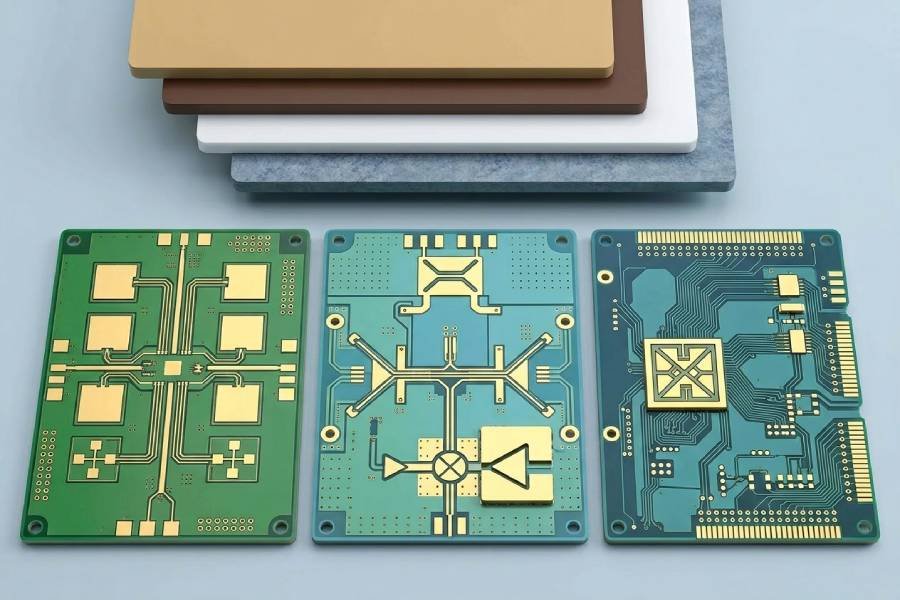
In advanced designs like flexible or rigid-flex PCBs, specialized copper foils are used for bendability without cracking. Electrodeposited (ED) copper suits fine-line circuits, while rolled-annealed (RA) copper provides better flexibility. PCBs can feature multiple layers— from 1 to 16 or more—with inner layers for signal routing and outer ones for component mounting.
Why Copper Foil Outshines Other Materials
Although alternatives like aluminum or silver exist, copper remains the standard in PCB manufacturing for several reasons:
- Cost-Effectiveness: It’s abundant and affordable, ideal for large-scale production.
- Resistance to Corrosion: Properly treated copper withstands oxidation, ensuring longevity.
- Compatibility: It works seamlessly with various substrates and solders, streamlining assembly.
Challenges such as thickness variations or impurities can occur, but quality control measures help address them effectively.
Conclusion: Copper Foil—The Heart of Reliable PCBs
Copper foil is far more than a simple material; it’s essential for creating efficient electrical pathways, managing heat, and forming strong bonds in PCBs. As electronics advance, its importance will only increase.
If you’re involved in PCB projects and need reliable manufacturing or assembly services—including prototypes, multilayer boards, rigid, flexible, or rigid-flex options, plus SMT, THT, turnkey assembly, component sourcing, and SMT stencils—consider partnering with JHYPCB, a China-based PCB manufacturer. Reach out at sales@pcbjhy.com for expert support.