


Table of Contents
Introduction
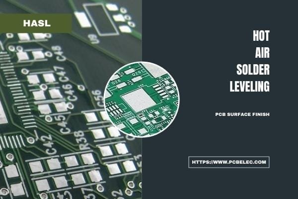
Hot Air Solder Leveling (HASL) is a trusted and cost-effective PCB surface finish widely used in electronics manufacturing. Known for its reliability and excellent solderability, HASL protects printed circuit boards (PCBs) from corrosion while ensuring robust performance. In this guide, we explore the HASL process, its benefits and drawbacks, and how it compares to lead-free HASL. Whether you’re a PCB manufacturer or an electronics enthusiast, this article provides insights to help you choose the right surface finish for your project.
What is Hot Air Solder Leveling (HASL)?
Hot Air Solder Leveling, commonly referred to as HASL, is a metallic surface finishing technique applied to the outermost layer of a printed circuit board. This process safeguards exposed copper surfaces from oxidation until components are placed and soldered. HASL typically involves a thin solder coating, traditionally composed of 63% lead and 37% tin, though lead-free options are now prevalent to comply with RoHS and REACH regulations.
HASL has been an industry-standard PCB surface treatment for decades due to its reliability, affordability, and superior solderability. Despite advancements in PCB complexity, HASL remains a go-to choice for manufacturers seeking durable and cost-effective surface finishes.
How Does the HASL Process Work?
The HASL process involves several stages to ensure a uniform and protective solder coating on the PCB. Below are the key steps:
- Precleaning the PCB
The PCB is thoroughly cleaned to remove contaminants, ensuring optimal adhesion of the solder coating. - Preheating the Board
The PCB is preheated to reduce thermal shock when it is immersed in molten solder. - Immersion in Molten Solder for Copper Coverage
The PCB is dipped into a molten solder bath (typically lead/tin or lead-free alloy), coating all exposed copper surfaces. This step ensures protection against corrosion. - Air Knife Leveling for Uniform Solder Deposit
High-pressure air knives blow hot air across the PCB surface to remove excess solder, creating a thin, uniform layer. This step enhances solderability and prevents uneven deposits. - Post-Cleaning
The PCB undergoes final cleaning to remove residual particles, ensuring a pristine surface ready for assembly.
The result is a reliable PCB surface finish that balances cost, durability, and performance.
What Are the Benefits of HASL for PCB Manufacturing?
HASL remains a popular choice due to its numerous advantages. Here are the key benefits:
- Cost-Effective: HASL is one of the most affordable PCB surface treatments compared to alternatives like ENIG or OSP.
- Widely Used: As an industry-standard process, HASL is well-established and trusted by manufacturers worldwide.
- Durable: The solder coating protects copper traces from corrosion, extending PCB lifespan.
- Excellent Solderability: HASL ensures strong solder joints, making it ideal for through-hole and surface-mount assemblies.
- Reworkable: Unlike some rigid surface finishes, HASL allows for easy adjustments during manufacturing.
- Reduced PCB Failure: HASL minimizes issues like short circuits, open circuits, and crossed signal lines, ensuring reliable performance.
To visualize how HASL compares to other surface finishes, see the chart below:

What Are the Drawbacks of HASL?
While HASL offers significant advantages, it also has limitations:
- Uneven Surfaces: HASL may produce inconsistent solder thickness, making it less suitable for fine-pitch components.
- Thermal Stress: High solder bath temperatures can stress PCBs, potentially reducing reliability.
- Not Ideal for Plated-Through Holes: HASL may cause solder bridging in complex PTH designs.
- Poor Wetting: In some cases, HASL surfaces exhibit suboptimal wetting compared to other finishes like ENIG.
Despite these drawbacks, HASL’s benefits often outweigh its limitations for many applications.
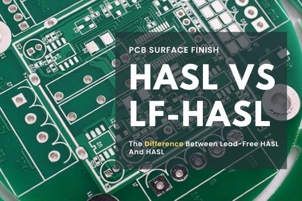
Lead-Free HASL vs. Traditional HASL: Key Differences
As environmental regulations like RoHS and REACH gain prominence, lead-free HASL has become a popular alternative to traditional HASL. Here’s how they differ:
- Solder Composition:
- Traditional HASL: 63% lead, 37% tin.
- Lead-Free HASL: 99.3% tin, 0.6% copper, ensuring RoHS compliance.
- Melting Point: Lead-free HASL has a higher melting point, requiring adjustments in the soldering process.
- Laminate Requirements: Lead-free HASL demands high-temperature laminates to withstand elevated processing temperatures.
- Applications: Lead-free HASL is preferred for eco-friendly projects, while traditional HASL suits less regulated applications.
Choosing between the two depends on your project’s regulatory and performance needs. Learn more about RoHS compliance for PCB manufacturing.
FAQ: Common Questions About HASL
Is HASL suitable for fine-pitch components?
HASL may not be ideal for fine-pitch components due to uneven solder surfaces. Consider ENIG for such applications.
How does HASL compare to other PCB surface finishes?
HASL is cost-effective and reliable but less precise than ENIG. Refer to the comparison chart above for details.
Is lead-free HASL more expensive?
Lead-free HASL may involve slightly higher material costs, but it remains affordable compared to other finishes.
Final Verdict on Hot Air Solder Leveling
Hot Air Solder Leveling (HASL) remains a cornerstone of PCB manufacturing due to its affordability, reliability, and excellent solderability. While it has limitations, such as uneven surfaces and thermal stress, its advantages make it a preferred choice for many applications. Whether you opt for traditional or lead-free HASL, this surface finish delivers consistent performance for a wide range of electronics projects.
Ready to implement HASL in your PCB manufacturing? Contact JHYPCB for expert guidance and high-quality PCB solutions. Explore our PCB manufacturing services.
Related Reading
Recommended Posts
Why PCB Prototyping is Essential for Cost-Effective Design Success
PCB prototyping is a critical step in electronics design, enabling you to validate functionality, reduce costs, and accelerate time-to-market. Learn how JHYPCB’s rapid PCB prototyping services help you test circuit performance, verify physical layouts, and enhance product reliability before full-scale production. Contact us to start your prototyping journey today.
RO4350B Dielectric Constant Explained: Parameters, Design Impact and Applications
This practical guide explains the RO4350B dielectric constant in real engineering terms—typical Dk and Df values, test conditions, design impact on impedance, loss and phase, plus when RO4350B is a better choice than FR‑4 for RF and microwave PCBs.
Choosing the Right PCB Surface Finish for Your Project in 2025
Discover the key factors in selecting a PCB surface finish, from HASL to ENIG, to optimize your project’s performance and budget. Read our guide now!
Precision Layer Alignment in Multilayer PCB Manufacturing
Achieving precise layer alignment in multilayer PCB manufacturing is critical for performance and reliability. Discover advanced techniques, prototyping challenges, quality control methods, and future trends driving high-density electronics.
High Frequency PCB Prototype to Production: RF PCB Prototyping and Manufacturing Guide
Moving a high frequency PCB from prototype to production is very different from scaling a standard FR‑4 design. RF PCB prototyping and manufacturing must handle specialized materials, tight impedance control, and more complex testing, so decisions made in early builds have a big impact on yield, cost, and performance at volume. This article explains each stage of the high frequency PCB prototype‑to‑production journey and gives practical tips to de‑risk your next RF ramp‑up.
Custom Flex PCB:Tailored Solutions for Your Applications
In today’s rapidly evolving electronics landscape, flexibility and adaptability are paramount. Custom flex PCBs offer a tailored solution that combines functionality with form factor flexibility. At [Company Name], we provide comprehensive custom flexible printed circuit board capabilities – from design expertise to material selection and quality testing. Explore the key advantages like compact lightweight designs, space optimization, durability and design freedom. Whether for wearable tech, medical devices, aerospace or automotive, leverage our custom flex PCB solutions for your innovative product needs. Request a quote now.


