Table of Contents
Introduction
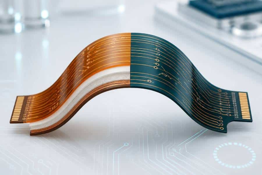
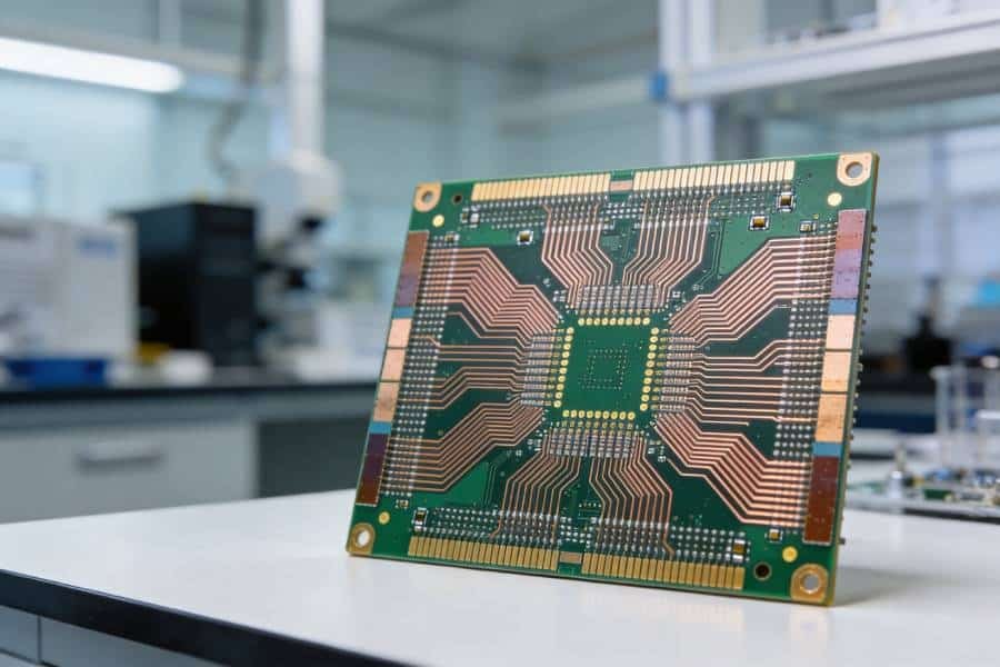
In the world of electronics, printed circuit boards (PCBs) are the unsung heroes powering everything from smartphones to coffee makers. These intricate boards form the backbone of modern devices, connecting components and enabling seamless electrical flow. At the heart of every PCB lies copper foil—a thin, versatile material that’s become the industry standard. But why is copper foil used in PCB manufacturing instead of alternatives like aluminum or tin? As a seasoned PCB manufacturer, we’ve seen firsthand how this choice impacts performance, reliability, and cost. In this article, we’ll dive into the reasons behind copper’s dominance, exploring its properties, applications, and role in the fabrication process. Whether you’re a designer, engineer, or hobbyist, understanding copper foil in PCB manufacturing can help you make informed decisions for your next project.
What Are PCBs Made Of?
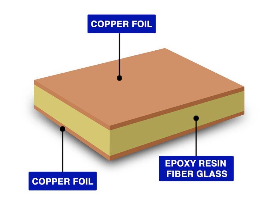
Before we get into the specifics of copper, let’s break down what makes up a typical PCB. At its core, a PCB consists of a substrate, often made from fiberglass reinforced with epoxy resin. This base provides structural support and insulation. On top (and sometimes below) sits a layer of copper foil, bonded to the substrate through lamination. This copper layer forms the conductive pathways that carry electrical signals.
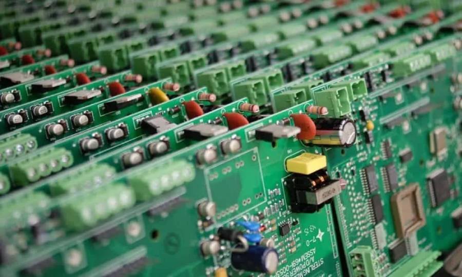
Once the base is ready, manufacturers add components like resistors, capacitors, transistors, diodes, and integrated circuits. To protect the board and aid in assembly, a solder mask—a usually green layer—is applied over the copper, leaving only the pads exposed for soldering. Finally, silkscreen printing adds labels and markings for easy identification.
This multi-layered structure ensures durability and functionality, but the copper foil is what truly brings it to life. Without it, the board would be just an inert slab, unable to conduct electricity efficiently.
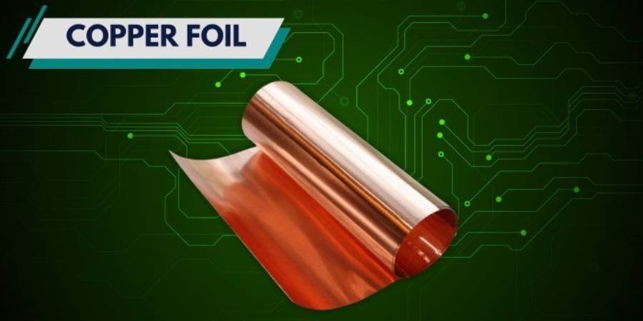
Why Copper Foil is Used in PCBs?
So, why use copper foil instead of aluminum in PCB production? The answer lies in copper’s exceptional properties. First and foremost, copper boasts superior electrical conductivity. It allows electrons to flow freely, minimizing signal loss or delay across the board. This is crucial for high-speed applications where even a slight lag can cause issues.
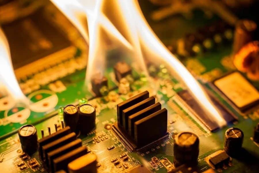
Copper’s thermal conductivity is another game-changer. As current flows through the PCB, heat builds up. Copper efficiently dissipates this heat, preventing uneven warming that could warp the board or damage components. In contrast, materials like aluminum or tin might lead to hotspots, reducing the board’s lifespan and reliability. For instance, aluminum has decent conductivity but oxidizes easily, forming a resistive layer that hampers performance over time.
At the atomic level, copper’s advantage stems from its free electrons—one per atom—that move effortlessly between atoms. This efficiency holds even in ultra-thin layers; just one ounce of copper can cover a square foot of substrate at a thickness of about 1.4 mils (35 micrometers). That’s why copper foil provides better signal integrity than other metals, making it ideal for everything from simple single-layer boards to complex multi-layer designs.
In practical terms, this means designers can incorporate heat sinks directly on the surface, enhancing thermal management in PCB design. Without copper’s robust properties, devices might overheat, leading to failures in critical applications like automotive electronics or medical equipment.
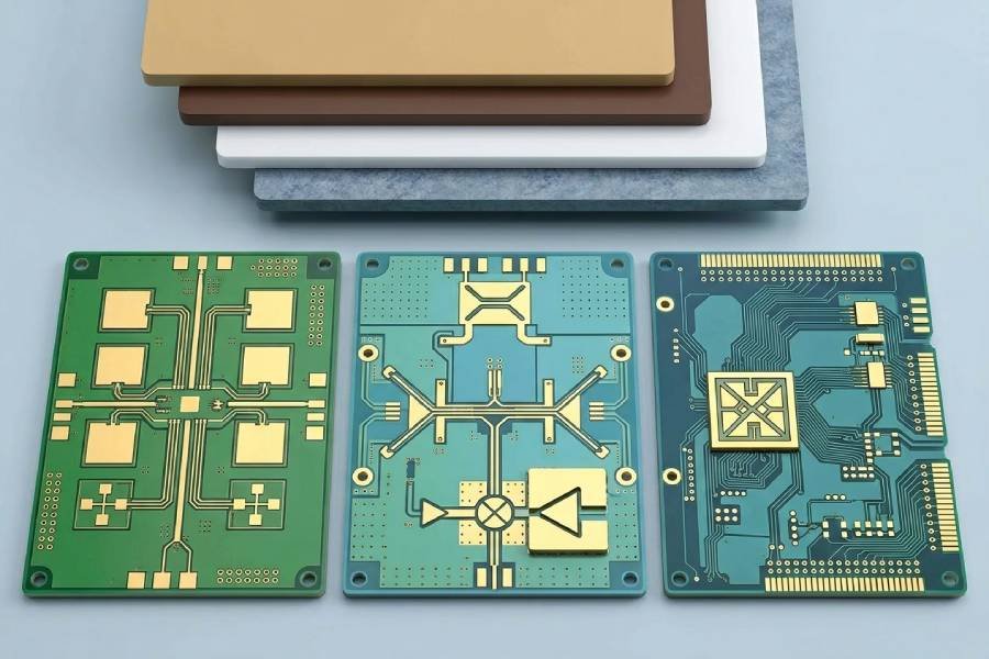
Copper and Other Precious Metals in PCBs
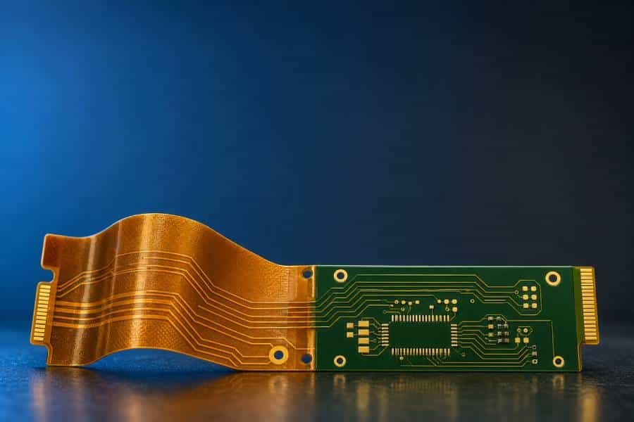
While copper is the star, it’s often paired with other metals to enhance specific features. You’ve probably noticed that PCBs aren’t just green—they feature golden, silver, or reddish hues on their surfaces. These come from immersion gold, immersion silver, and copper clad laminates.
Immersion gold, for example, is applied to connector edges and component pads. This thin layer of real gold prevents corrosion and ensures reliable soldering over time. It’s pricier but extends the board’s life, especially in harsh environments.
Immersion silver offers a cost-effective alternative, improving connectivity while keeping expenses down. It’s commonly used in automotive and peripheral computer boards, where budget and performance must balance.
Then there’s the copper clad laminate—the reddish layer that’s the most ubiquitous. This forms the base conductive material, ensuring circuits connect seamlessly. Benefits of copper clad laminate in multilayer PCBs include strong adhesion and resistance to delamination during thermal cycles.
Together, these metals create a robust ecosystem: copper for core conductivity, gold and silver for protection. This combination is why PCBs can handle diverse demands without compromising quality.
How Copper Foil is Used in PCBs
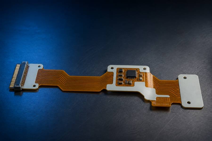
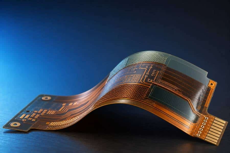
Copper foil’s versatility shines in its various applications within a PCB. One key use is in PCB traces—the conductive paths that route signals between components. Think of a trace like a highway: it needs to be wide enough for traffic (current), thick enough to withstand pressure (voltage), and made of durable material to avoid breakdowns.
Trace components include the copper network itself, wires, insulation, fuses, and attached parts. The width and thickness of these traces are critical. For example, wider traces handle higher currents without overheating, while thickness affects overall current carrying capacity. How copper foil thickness affects PCB current carrying capacity is a common design consideration—thinner foils suit low-power apps, while thicker ones are for high-current needs.
PCB thickness also plays a role, influencing balance and component mounting. But it’s the copper that ensures smooth current flow, thanks to those free electrons facilitating efficient transmission.
Without proper traces, electricity couldn’t navigate the board effectively. Imagine trying to drive across a city without roads—that’s a PCB without copper traces.
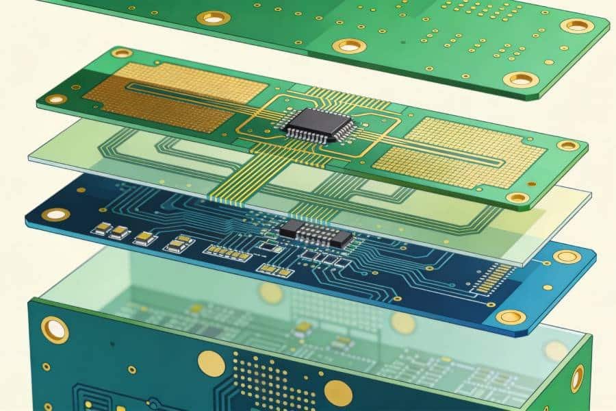
The PCB Manufacturing Process Involving Copper Foil
Understanding copper’s role becomes clearer when we look at the fabrication process. While methods vary slightly, the core steps remain consistent, with copper foil integral throughout.
It starts with creating the substrate from fiberglass and resin. Next, copper foil layers are laminated onto one or both sides. Patterns are then defined using photoresist and etching—excess copper is removed to form traces and pads.
The board is cleaned in a chemical bath to remove residues, followed by applying the solder mask for protection. Silkscreen adds markings, and finally, components are mounted and soldered, often via surface mount technology (SMT) or through-hole technology (THT).
Testing ensures everything works, from continuity to functionality. Copper etching in PCB manufacturing is a precise step, where the foil’s quality directly impacts the final product’s accuracy. A step-by-step guide to using copper foil in PCB production highlights its necessity: without it, there’s no conductive foundation.
Conclusion
In summary, copper foil is indispensable in PCB manufacturing due to its unmatched electrical and thermal conductivity, efficiency in thin layers, and compatibility with other metals. It outperforms alternatives like aluminum or tin, ensuring reliable signal transmission and heat dissipation. From traces to laminates, copper enables the complex interconnections that power our daily devices. Without it, we’d be in a world without smartphones, laptops, or even basic appliances.
If you’re planning a PCB project and need expert guidance on materials like copper foil, reach out to us at sales@pcbjhy.com. As a reliable PCB manufacturer offering services from prototyping to full assembly, we’re here to help bring your ideas to life. For more insights, check our related articles on PCB materials and RA copper vs. ED copper.