Table of Contents
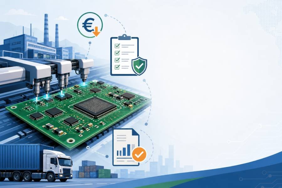
At JHYPCB, we’ve been at the forefront of PCB manufacturing and assembly for years, helping clients worldwide bring their innovative ideas to life. As a leading China-based PCB manufacturer, we specialize in everything from PCB prototypes to full-scale production, including single-sided, double-sided, and multilayer PCBs, as well as rigid, flexible, and rigid-flex options. Our PCB assembly services cover SMT, THT, mixed technology, turnkey solutions, component sourcing, and SMT stencils. If you’re exploring double sided PCB assembly, you’re in the right place—this guide will walk you through the essentials, processes, and tips to make informed decisions. Whether you’re a hobbyist prototyping a new gadget or an engineer designing complex electronics, understanding double sided PCB assembly can elevate your projects. Let’s dive in.
What is Double Sided PCB? Basics and Components
If you’ve ever wondered, “What is double sided PCB?” you’re not alone. A double sided PCB, also known as a double sided PCB board, is a type of printed circuit board with conductive copper layers on both the top and bottom sides. This design allows for more intricate circuitry compared to single-sided boards, where components are only mounted on one side.
The key difference between single sided PCB and double sided PCB lies in functionality and complexity. Single-sided PCBs are simpler and cheaper, ideal for basic applications like calculators or remote controls. In contrast, double sided PCBs enable higher component density and better signal routing through vias (small holes connecting the layers), making them perfect for more advanced devices.
To break it down further, here are the core components of a double sided PCB board:
- Substrate: The foundational layer, typically made from fiberglass-reinforced epoxy (FR4), providing mechanical strength and insulation.
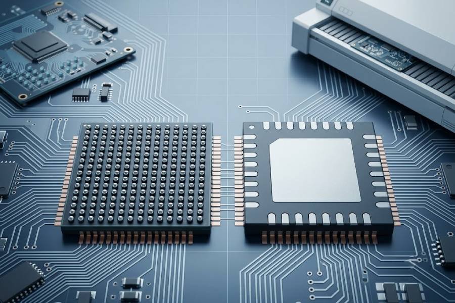
- Copper Layers: Thin sheets of copper foil on both sides, etched to form traces, pads, and circuits.
- Solder Mask: A protective coating over the copper to prevent oxidation and short circuits during soldering.
- Silkscreen: Printed markings for component labels, polarity indicators, and assembly instructions.
Visualizing this? Imagine a double sided PCB assembly diagram: the top layer might host surface-mount devices (SMDs), while the bottom accommodates through-hole components, connected via plated vias. At JHYPCB, we often recommend starting with a prototype to test these layouts—our double sided PCB board prototype services ensure quick iterations without breaking the bank.

Advantages and Disadvantages of Double Sided PCBs
Double sided PCBs offer a compelling balance of performance and compactness, but like any technology, they come with trade-offs. Let’s explore the pros and cons to help you decide if they’re right for your project.
Advantages
- Higher Component Density: By utilizing both sides, you can pack more components into a smaller footprint, ideal for space-constrained devices like smartphones or wearables.
- Improved Signal Integrity: Vias allow for shorter trace lengths, reducing noise and enhancing performance in high-speed applications.
- Cost-Effective for Medium Complexity: Compared to multilayer boards, double sided PCBs are more affordable while supporting moderately complex designs.
- Versatility: They support both SMT and THT assembly, making them adaptable for various manufacturing needs.
In our experience at JHYPCB, clients often choose double sided options for prototypes because they strike a great balance—offering the density of multilayer without the added cost.
Disadvantages of Double Sided PCB
No solution is perfect, and double sided PCBs have their challenges:
- Increased Manufacturing Complexity: Aligning components on both sides requires precise drilling and plating, which can raise costs if not managed well.
- Thermal Management Issues: Heat dissipation can be trickier without additional layers for ground planes.
- Soldering Challenges: Double sided SMD soldering demands careful techniques to avoid damaging components on the opposite side.
- Limited for Ultra-High Density: For extremely complex circuits, multilayer PCBs might be necessary.
Despite these disadvantages of double sided PCB, proper design can mitigate most issues. For instance, incorporating thermal vias early in the process helps with heat flow.
To illustrate the comparison, here’s a quick table on double sided vs single sided PCB:
| Aspect | Single Sided PCB | Double Sided PCB |
|---|---|---|
| Component Placement | One side only | Both sides |
| Complexity | Low (basic circuits) | Medium (advanced routing) |
| Cost | Lower | Moderate |
| Size | Larger for same functionality | More compact |
| Applications | Simple toys, LEDs | Consumer electronics, controls |
This double sided vs single sided PCB overview shows why many engineers upgrade to double sided for better efficiency.
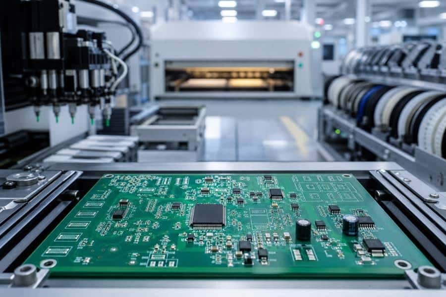
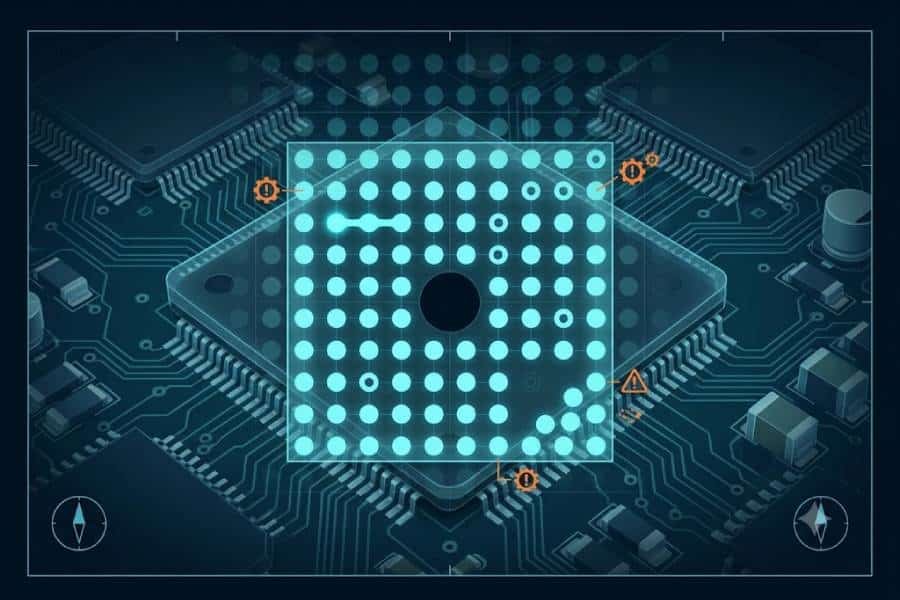
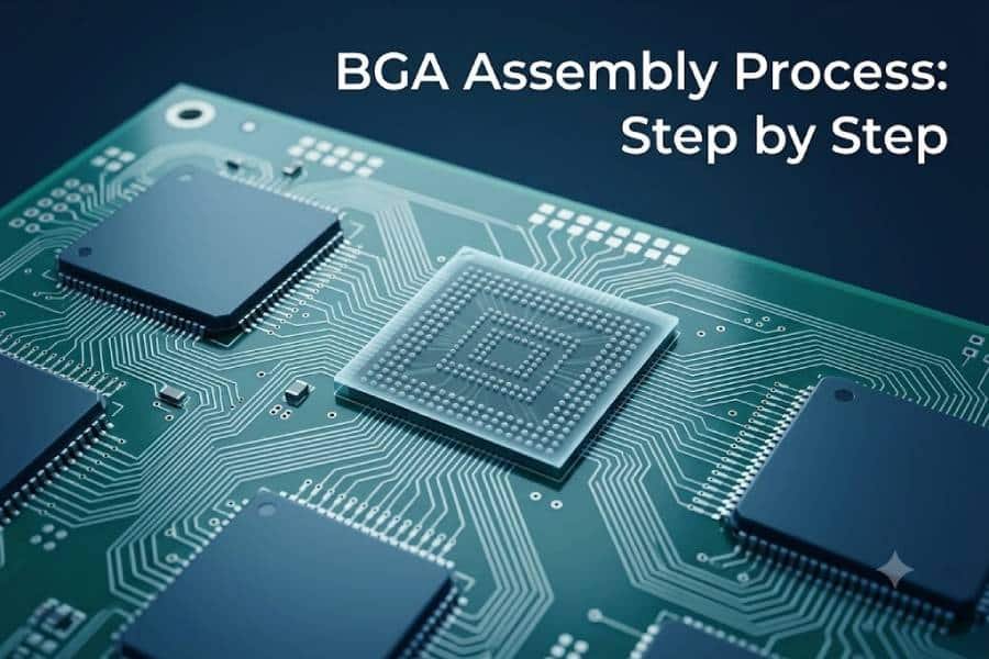
Double Sided PCB Assembly Process
The double sided PCB assembly process is where the magic happens—transforming a bare board into a functional circuit. At JHYPCB, we handle this end-to-end, from design review to final testing. Here’s a step-by-step breakdown.
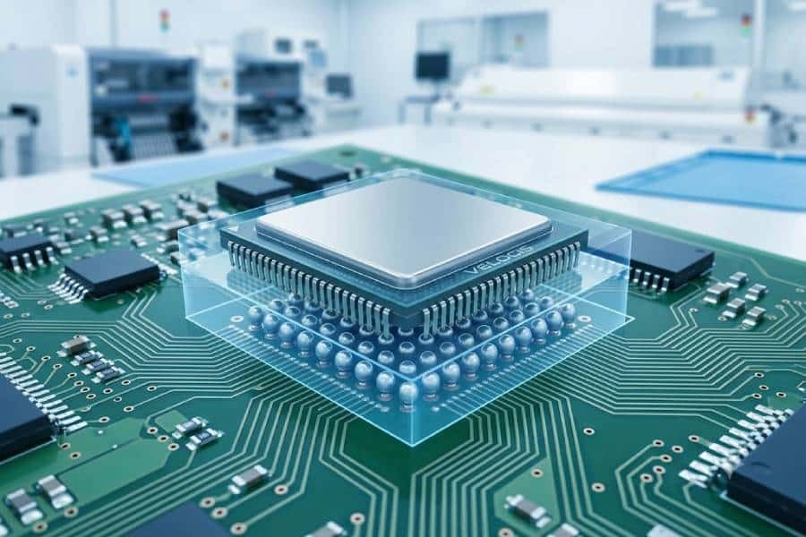
Surface Mount Technology (SMT) for Double Sided SMT Assembly
SMT is the go-to for high-volume, compact assemblies. In double sided SMT assembly:
- Stencil Printing: Apply solder paste to pads on one side using a laser-cut stencil.
- Pick and Place: Automated machines place SMD components precisely.
- Reflow Soldering: Heat the board in a reflow oven to melt the paste, securing components.
- Flip and Repeat: Turn the board over and repeat for the other side, often using adhesives to hold bottom-side components during reflow.
Double sided SMD soldering requires expertise to prevent tombstoning (components lifting) or voids.

Through-Hole Technology (THT) and Mixed Assembly
For components needing mechanical strength, like connectors:
- Component Insertion: Insert leads into drilled holes.
- Wave Soldering: Pass the board over molten solder waves to bond leads. In mixed tech, combine SMT on one side with THT on the other for optimal results.

Double Sided PCB Soldering Techniques
Wondering how to use double sided PCB board effectively? For manual double sided PCB soldering:
- Use a soldering iron with fine tips for precision.
- Solder one side first, then flip—apply flux to improve flow.
- For prototypes, hand soldering works, but for production, reflow or wave is essential.
Our turnkey PCB assembly at JHYPCB includes component sourcing, ensuring compatibility and quality throughout the double sided PCB manufacturing process.
Design Considerations for Double Sided PCB Prototyping
Designing a double sided PCB board prototype demands attention to detail to avoid costly revisions. Start with robust software like Altium or KiCad for schematics and layouts.
Key tips:
- Layout Optimization: Place high-frequency components close to minimize trace lengths. Use ground planes on one side for shielding.
- Via Placement: Strategically position vias to connect layers without obstructing components.
- Edge Clearance: Keep components away from edges to ease soldering and assembly.
Thermal management is crucial—incorporate vias under heat-generating parts to dissipate warmth. For double sided PCB prototyping, we at JHYPCB offer fast-turn services, often delivering prototypes in days, with full DFM (Design for Manufacturability) checks to catch issues early.
Applications and Use Cases
Double sided PCBs shine in diverse fields due to their balance of size and capability.
- Consumer Electronics: From tablets to smart home devices, where compactness is key.
- Industrial Control Systems: Robust for harsh environments, like automation panels or sensors.
- Medical Devices: Compact designs for wearables monitoring health metrics.
- Automotive: In dashboards or ECUs, handling vibrations and temperatures.
At JHYPCB, we’ve assembled double sided boards for everything from IoT prototypes to industrial controllers, proving their versatility.
Choosing a Double Sided PCB Assembly Manufacturer
Selecting the right partner is vital. Look for:
- Experience: Proven track record in double sided PCB assembly manufacturers.
- Capabilities: Full services like SMT, THT, and prototyping.
- Quality Standards: IPC-certified processes.
- Turnaround and Cost: Competitive pricing with quick delivery.
Why JHYPCB? We’re not just another manufacturer—we’re your end-to-end solution. Our China-based facility ensures cost efficiency without compromising quality. We offer double sided PCB assembly process customization, including other double sided assembly alternatives with better lead times. Plus, our component sourcing service saves you time and hassle. Ready to start? Email us at sales@pcbjhy.com for a free quote.
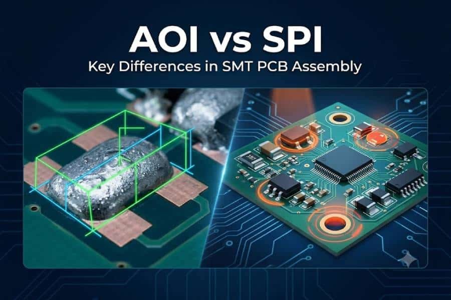
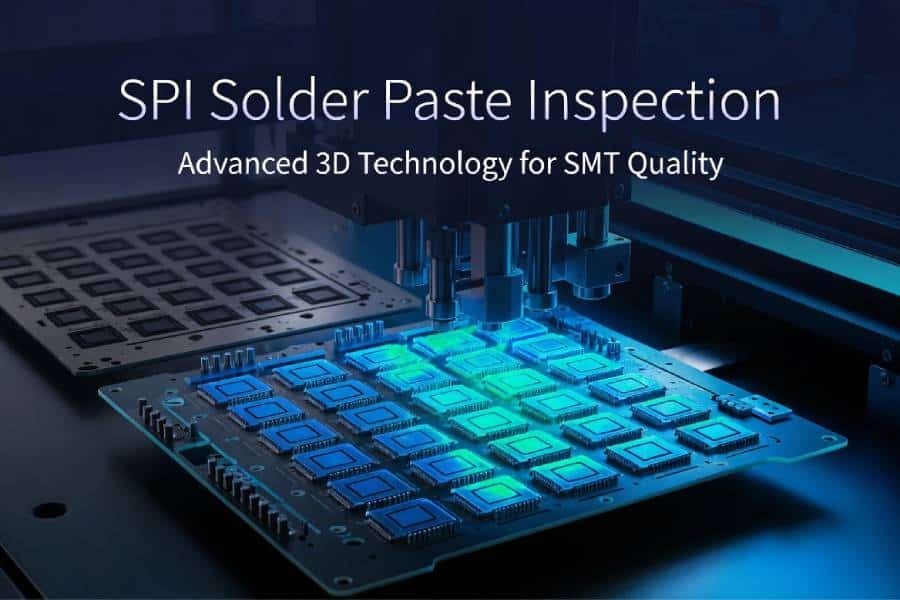
Quality Assurance, Testing, and Common Challenges
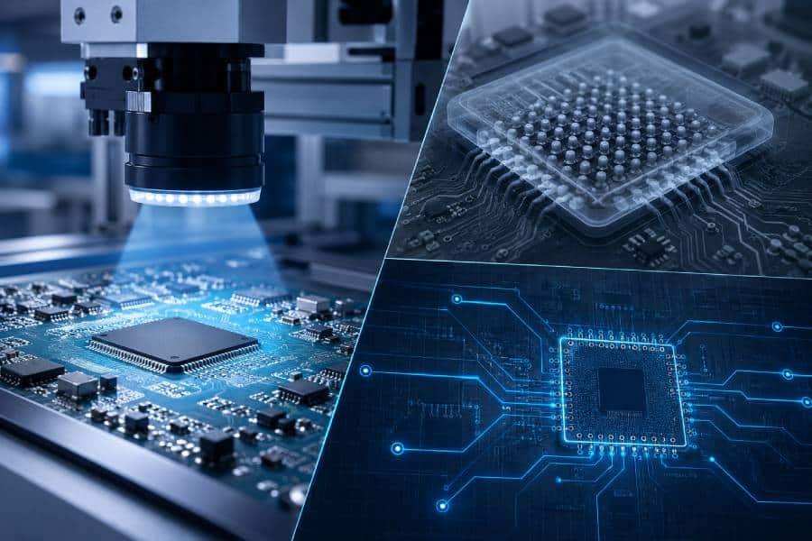
Quality is non-negotiable in PCB assembly. At JHYPCB, we employ:
- Automated Optical Inspection (AOI): Scans for defects like misalignments.
- Functional Testing: Simulates real-world use to verify performance.
- In-Circuit Testing (ICT): Checks electrical integrity.
Common challenges include alignment errors in double sided assembly or solder bridges. Overcome them with precise stencils and experienced technicians. For resources, we provide double sided PCB assembly PDF guides upon request.
Conclusion
Double sided PCB assembly is a powerhouse for modern electronics, offering density, performance, and versatility that single-sided boards can’t match. From understanding the basics to mastering the assembly process, this guide equips you with the knowledge to succeed. While there are disadvantages like added complexity, the benefits far outweigh them for most applications.
At JHYPCB, we’re passionate about turning your designs into reality. Whether you need a double sided PCB board prototype, full manufacturing, or turnkey assembly, our team is here to help. Contact us today at sales@pcbjhy.com to discuss your project and get started on optimized, high-quality PCBs. Let’s build something amazing together!