Single-layer PCB vs. Double-sided PCB: How to Choose?

Discover the differences between single-sided, double-sided, and multilayer PCBs with JHYPCB’s expert guide. Learn their applications, advantages, and how to choose the right PCB for your project.
single-layer PCB vs.double-sided PCB

Table of Contents

Introduction

Printed Circuit Boards (PCBs) are the foundation of modern electronics, serving as the critical platform that connects and powers components in devices ranging from simple gadgets to sophisticated industrial systems. Whether you’re a hobbyist designing a prototype, an engineer developing a consumer product, or a manufacturer scaling production, choosing the right PCB type is a pivotal decision that impacts performance, cost, and reliability. Among the most common options are single-layer PCBs (also known as single-sided PCBs), double-sided PCBs, and multilayer PCBs, each offering unique advantages tailored to specific project needs.

At JHYPCB, we’ve been empowering global clients with high-quality PCB manufacturing solutions for years, offering everything from single-sided and double-sided PCBs to advanced multilayer boards (up to 32 layers) and flexible PCBs. Our expertise ensures that you get the right PCB for your application, whether it’s a cost-effective solution for a simple circuit or a complex design for cutting-edge technology.

In this comprehensive guide, we’ll dive into the differences between single-sided, double-sided, and multilayer PCBs, exploring their structures, applications, advantages, and limitations. By the end, you’ll have a clear understanding of which PCB type suits your project and how to make an informed choice. Let’s get started by defining these PCB types and uncovering what sets them apart.

What Are Single-Sided and Double-Sided PCBs?

Understanding the structure and functionality of single-sided and double-sided PCBs is essential for selecting the right board for your project. Both types share a common foundation but differ significantly in design, capabilities, and applications. Below, we break down their construction, component mounting methods, and key characteristics, with insights from JHYPCB, a leading manufacturer of high-quality PCBs.

Single-Sided PCBs

A single-sided PCB, also known as a single-layer PCB, consists of a single conductive layer on one side of an insulating substrate, typically FR-4, a durable fiberglass-epoxy composite. The conductive layer is made of a thin copper foil, which is etched to form conductive traces and pads. This layer is coated with a solder mask for protection against oxidation and short circuits, and often a silkscreen layer is added for labeling components or identifiers.

Components on single-sided PCBs are mounted using one of two methods:

  • Through-hole technology: Components are placed on the top (component) side, with their leads passing through drilled holes to the bottom (solder) side, where they are soldered to copper pads or traces.

  • Surface-mount technology (SMT): Components are directly attached to the solder side, eliminating the need for drilled holes, which simplifies assembly for compact designs.

Single-sided PCBs are best suited for simple circuits with low component density, such as those found in basic consumer electronics, LED lighting, or HVAC control systems. Their straightforward design makes them a cost-effective choice for hobbyists and manufacturers alike.

A Single-layer Aluminum PCB

Double-Sided PCBs

A double-sided PCB features conductive copper layers on both sides of the FR-4 substrate, effectively doubling the available space for traces and components. These boards use viasplated through-holes that create electrical connections between the top and bottom layers. This allows for more complex routing and higher component density compared to single-sided PCBs.

Component mounting on double-sided PCBs is more versatile:

    • Through-hole components are typically placed on the top side, with leads passing through vias to connect to traces on either side.
    • Surface-mount components can be attached to either or both sides, enabling compact designs.
    • Mixed mounting: A combination of through-hole and surface-mount components is common, optimizing space and functionality.

Double-sided PCBs are ideal for complex applications, such as smartphones, automotive electronics, and medical devices, where intricate circuitry and compact layouts are critical. The use of vias enhances design flexibility, making these boards a go-to choice for advanced projects.

Double-sided PCBs
Double-sided PCBs

Quick Comparison Table

To summarize the structural differences:

FeatureSingle-Sided PCBDouble-Sided PCB
Conductive LayersOne (bottom/solder side)Two (top and bottom sides)
Component MountingThrough-hole or SMT on one sideThrough-hole and/or SMT on both sides
ViasNonePlated through-holes for connectivity
Circuit ComplexitySimple, low-density circuitsComplex, high-density circuits
Typical Use CasesCalculators, HVAC controlsSmartphones, automotive systems
the difference between single sided pcb and double sided pcb structures
The difference between single-sided PCB and double-sided PCB structures

Key Differences Between Single-Sided and Double-Sided PCBs

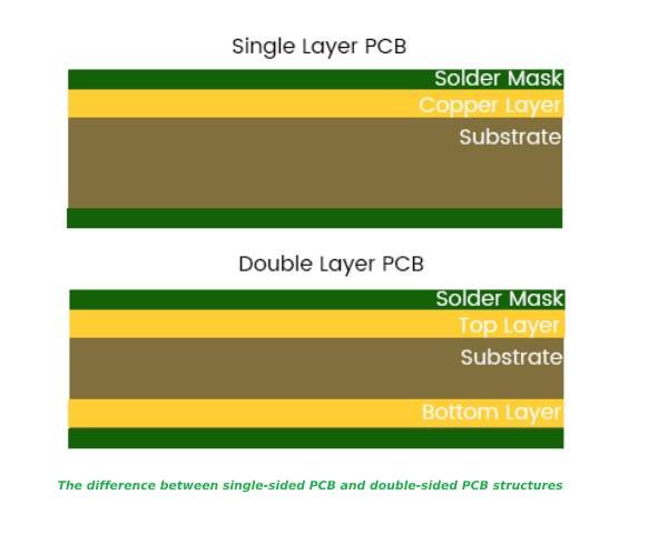
While single-sided and double-sided PCBs share the same foundational materials, such as FR-4 substrates and copper conductive layers, their differences in design, functionality, and manufacturing processes significantly impact their suitability for various applications. Understanding these distinctions is crucial for engineers, hobbyists, and manufacturers to select the right PCB for their projects. Below, we explore the key differences in design complexity, cost, applications, and manufacturing processes, drawing on the expertise of JHYPCB.

1. Design Complexity

Single-Sided PCBs are limited to a single conductive layer, which restricts the routing of traces to one side of the board. This makes circuit design more challenging, as designers must avoid overlapping traces and ensure all connections fit within the limited space. For complex circuits, this often results in larger board sizes to accommodate all components and connections.

Double-Sided PCBs, by contrast, offer conductive layers on both sides of the substrate, connected through vias (plated through-holes). This doubles the available routing space, allowing for more intricate circuit designs and higher component density. Designers can place components on both sides and route traces more efficiently, reducing board size and enabling compact, sophisticated layouts.

Key Takeaway: Single-sided PCBs suit simple, low-density designs, while double-sided PCBs excel in complex circuits requiring flexible routing.

2. Cost

Single-Sided PCBs are more cost-effective due to their simpler construction. With only one copper layer to etch and no need for vias, the manufacturing process involves fewer steps, reducing material and labor costs. This makes single-sided PCBs an economical choice for budget-conscious projects, such as hobbyist prototypes or mass-produced consumer electronics.

Double-Sided PCBs are more expensive because they require additional manufacturing steps, including drilling and plating vias to connect the two conductive layers. The increased material usage and complexity of the process drive up production costs, but the enhanced functionality often justifies the investment for advanced applications.

Key Takeaway: Single-sided PCBs are ideal for cost-sensitive projects, while double-sided PCBs offer greater value for performance-driven designs.

3. Applications

Single-Sided PCBs are commonly used in applications where simplicity and reliability are paramount. Examples include:

  • HVAC Systems: Control boards for heating and cooling systems, where basic circuitry is sufficient.
  • LED Lighting: Simple driver circuits for LED strips or bulbs.
  • Basic Consumer Electronics: Devices like calculators, remote controls, or toys with minimal components.

Double-Sided PCBs are preferred for more advanced applications requiring higher component density and complex routing. Examples include:

  • Smartphones: Compact designs with multiple components, such as processors and sensors.
  • Automotive Electronics: Control units for engine management or infotainment systems.
  • Medical Devices: Diagnostic equipment requiring precise, high-density circuitry.

Key Takeaway: Single-sided PCBs are suited for straightforward, cost-effective applications, while double-sided PCBs support complex, high-performance electronics.

4. Manufacturing Process

The manufacturing process for Single-Sided PCBs is relatively simple:

  • A single copper layer is laminated onto the FR-4 substrate.
  • The copper is etched to form traces and pads.
  • A solder mask is applied for protection, followed by optional silkscreening for labeling.

In contrast, Double-Sided PCBs involve a more complex process:

  • Copper is laminated on both sides of the substrate.
  • Vias are drilled and plated to establish electrical connections between layers.
  • Both sides are etched, coated with a solder mask, and silkscreened if needed.

The additional steps for double-sided PCBs require advanced equipment and quality control, which JHYPCB ensures through its state-of-the-art facilities and rigorous testing.

Key Takeaway: Single-sided PCBs are easier and cheaper to manufacture, while double-sided PCBs demand more sophisticated processes for enhanced functionality.

Bar chart comparing single-sided and double-sided PCBs in cost, complexity, and application suitability.

Bar chart comparing single-sided and double-sided PCBs in cost, complexity, and application suitability.

Why These Differences Matter

The choice between single-sided and double-sided PCBs hinges on balancing design requirements, budget constraints, and application needs. For instance, a hobbyist building a simple LED circuit may prioritize the low cost of a single-sided PCB, while an engineer designing a compact IoT device may opt for a double-sided PCB to accommodate a dense layout. By understanding these differences, you can make informed decisions that optimize performance and cost.

Advantages and Disadvantages

When deciding between single-sided and double-sided PCBs, understanding their respective strengths and limitations is critical. Each type offers unique benefits that make it suitable for specific applications, but also comes with trade-offs that can impact your project’s design, cost, and performance. Below, we outline the advantages and disadvantages of single-sided and double-sided PCBs, providing real-world examples to guide your decision-making. At JHYPCB, we leverage our expertise in PCB manufacturing to help you choose the optimal solution for your needs.

Single-Sided PCBs

Advantages

  • Cost-Effective: Single-sided PCBs are the most economical option due to their simple design and manufacturing process. With only one conductive layer, fewer materials and simpler production steps (e.g., single-sided etching) reduce costs, making them ideal for budget-conscious projects like hobbyist prototypes or mass-produced consumer goods.

  • Easy to Manufacture: The straightforward design of single-sided PCBs simplifies the production process, requiring less specialized equipment. This makes them accessible for hobbyists crafting PCBs at home or manufacturers aiming for quick turnaround times.

  • Reliable for Simple Applications: Single-sided PCBs are proven in low-complexity applications where reliability is key. Their robust, uncomplicated design minimizes points of failure, ensuring consistent performance in devices like HVAC control boards or basic LED circuits.

Disadvantages

  • Limited Routing Space: With only one conductive layer, routing traces can be challenging, especially for circuits with many components. This often requires larger board sizes to accommodate all connections, which may not suit compact designs.
  • Unsuitable for Complex Circuits: Single-sided PCBs struggle to support high-density or intricate circuits, limiting their use in advanced applications like modern consumer electronics or high-speed systems.

Example: A single-sided PCB is perfect for a basic calculator, where a small number of components and simple connections keep costs low and manufacturing straightforward.

Double-Sided PCBs

Advantages

  • Greater Design Flexibility: With conductive layers on both sides connected by vias, double-sided PCBs allow for more complex routing and compact layouts. This enables designers to place components on both sides, optimizing space and supporting intricate circuit designs.
  • Higher Component Density: Double-sided PCBs can accommodate more components in a smaller footprint, making them ideal for applications requiring dense circuitry, such as smartphones or automotive control modules.
  • Versatile Applications: The ability to handle complex circuits makes double-sided PCBs suitable for a wide range of industries, including consumer electronics, automotive, medical, and industrial systems, where performance and space efficiency are critical.

Disadvantages

  • Higher Manufacturing Costs: The additional conductive layer, drilling, and plating of vias increase material and production costs compared to single-sided PCBs. This can be a limiting factor for budget-sensitive projects.
  • Complex Manufacturing Process: Producing double-sided PCBs requires advanced equipment and precise processes, such as via plating and dual-sided etching, which can increase lead times and demand higher quality control.

Example: A double-sided PCB is essential for a smartphone, where a compact design must integrate multiple components like processors, sensors, and connectivity modules.

Balancing Trade-Offs

The choice between single-sided and double-sided PCBs depends on your project’s priorities. If cost and simplicity are paramount, single-sided PCBs offer a reliable, budget-friendly solution. For projects requiring compact, high-performance designs, double-sided PCBs provide the necessary flexibility and density. At JHYPCB, we offer both options, along with multilayer and flexible PCBs, ensuring you get a tailored solution that meets your technical and budgetary needs.

How to Choose Between Single-Sided and Double-Sided PCBs

Selecting the right PCB for your project is a critical decision that balances performance, cost, and manufacturing feasibility. Whether you’re a hobbyist prototyping a simple circuit, an engineer designing a compact device, or a manufacturer optimizing for scale, understanding key factors can guide you to the best choice. Below, we outline the primary considerations—project requirements, budget, manufacturing capabilities, and application type—and provide a practical checklist to streamline your decision-making process. At JHYPCB, we’re here to support you with tailored PCB solutions for any project.

1. Project Requirements

The complexity and performance needs of your circuit are the starting point for choosing a PCB type:

  • Circuit Complexity: Single-sided PCBs are ideal for simple circuits with few components and straightforward connections, such as those in LED drivers or basic control modules. Double-sided PCBs, with their dual conductive layers and vias, support more complex circuits requiring intricate routing, such as microcontrollers or IoT devices.
  • Component Density: If your design demands a high number of components in a compact space, double-sided PCBs allow for placement on both sides, reducing board size. Single-sided PCBs may require larger boards to accommodate all components, which can be a limitation for space-constrained applications.
  • Performance Needs: For high-speed or high-frequency circuits (e.g., RF modules or data processing units), double-sided PCBs offer better signal integrity due to flexible routing and grounding options. Single-sided PCBs are sufficient for low-frequency, basic applications.

2. Budget

Cost is a major factor in PCB selection:

  • Single-Sided PCBs: These are the most budget-friendly option due to their simpler design and manufacturing process. They require fewer materials and less complex production steps, making them ideal for cost-sensitive projects like hobbyist prototypes or mass-produced consumer electronics.
  • Double-Sided PCBs: The additional conductive layer, vias, and manufacturing processes increase costs. However, the investment is justified for applications where performance, compactness, or reliability outweigh budget constraints.

Tip: For large-scale production, the cost difference may be offset by the efficiency and performance gains of double-sided PCBs. Consult with JHYPCB to explore cost-optimization strategies.

3. Manufacturing Capabilities

Your access to manufacturing resources influences the choice:

  • Hobbyists: Single-sided PCBs are easier to produce at home using basic etching and soldering techniques, making them a popular choice for DIY projects. The simpler process reduces the need for specialized equipment.
  • Professional Manufacturing: Double-sided PCBs require advanced equipment for drilling, plating vias, and dual-sided etching. Professional manufacturers like JHYPCB ensure precision and quality for both single-sided and double-sided PCBs, making them accessible for complex projects without compromising reliability.

4. Application Type

The intended use of your PCB shapes the decision:

  • Consumer Electronics: Devices like smartphones, tablets, or wearables often require double-sided PCBs to accommodate dense, high-performance circuits in compact designs.
  • Industrial Systems: Applications like HVAC controls or motor drivers often use single-sided PCBs for their cost-effectiveness and reliability in simple, robust systems.
  • Automotive and Medical: These industries demand double-sided PCBs for their ability to handle complex, high-reliability circuits in safety-critical applications.

Decision-Making Checklist

To simplify your choice, use this checklist:

  • Is your circuit simple with minimal components? → Choose a single-sided PCB for cost savings and ease of production.
  • Do you need a compact design with high component density? → Opt for a double-sided PCB to maximize space and flexibility.
  • Is your budget limited? → Single-sided PCBs are the most economical choice.
  • Does your project require high performance or complex routing? → Double-sided PCBs (or multilayer PCBs for advanced needs) are better suited.
  • Are you manufacturing at home or with limited resources? → Single-sided PCBs are easier for DIY production.
  • Need professional-grade quality? → Partner with JHYPCB for reliable, high-quality PCB solutions.

Making the Right Choice with JHYPCB

Choosing between single-sided and double-sided PCBs requires aligning your project’s technical and financial goals. At JHYPCB, we offer both single-sided and double-sided PCBs, as well as multilayer and flexible options, tailored to your specific needs. Our expertise ensures high-quality boards that meet industry standards, whether you’re building a simple prototype or a complex system. Contact us today for a free quote and expert guidance.

When to Consider Multilayer PCBs

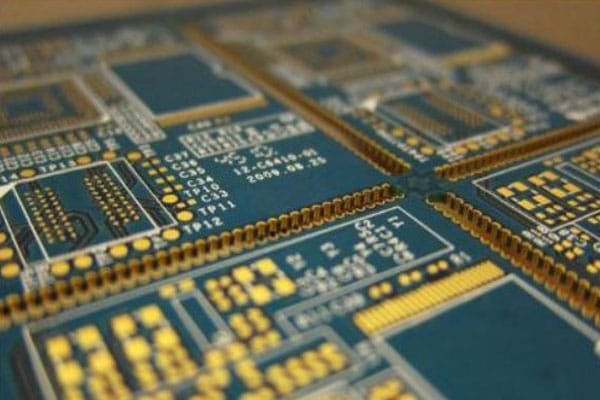
While single-sided and double-sided PCBs are suitable for many applications, there are scenarios where their limitations in routing space, component density, or performance fall short. This is where multilayer PCBs, with three or more conductive layers, become the ideal choice. These advanced boards offer enhanced functionality for complex, high-performance electronics. As a leading PCB manufacturer, JHYPCB specializes in producing multilayer PCBs (up to 32 layers) and flexible PCBs, catering to industries with demanding requirements. Below, we explore when to opt for multilayer PCBs and how they address the shortcomings of single-sided and double-sided boards.

Why Choose Multilayer PCBs?

Multilayer PCBs consist of multiple conductive copper layers separated by insulating substrates, typically FR-4, bonded together. These layers are interconnected through vias (plated through-holes or blind/buried vias), enabling intricate routing and high component density. The key advantages include:

  • Increased Routing Capacity: Multiple layers provide ample space for complex circuit designs, reducing the need for large board sizes.
  • Enhanced Signal Integrity: Dedicated layers for power and ground planes improve signal performance, crucial for high-speed circuits.
  • Compact Design: Multilayer PCBs support dense component placement, ideal for space-constrained devices.
  • Improved EMI Shielding: Additional layers can be used for shielding, reducing electromagnetic interference in sensitive applications.

Diagram of multilayer PCB structure showing multiple copper layers, FR-4 substrate, and vias.

When Single-Sided and Double-Sided PCBs Are Insufficient

Single-sided and double-sided PCBs are excellent for simple to moderately complex projects, but they may not meet the needs of advanced applications. Consider multilayer PCBs in the following scenarios:

  • High-Speed Circuits: Applications like telecommunications equipment, servers, or high-frequency RF devices require multilayer PCBs to manage signal integrity and minimize crosstalk. For example, a 5G base station relies on multilayer boards to handle rapid data transmission.
  • Compact, High-Density Designs: Devices such as wearables, smartphones, or medical implants demand small footprints with numerous components. Multilayer PCBs enable compact layouts without sacrificing functionality.
  • Complex Functionality: Projects with intricate circuitry, such as advanced computing systems or automotive ECUs (electronic control units), benefit from the additional routing layers to accommodate complex connections.
  • High Reliability Requirements: Industries like aerospace, medical, and military often require multilayer PCBs for their durability and ability to support redundant connections, ensuring reliability in critical systems.

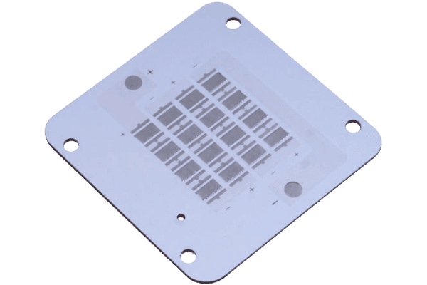
Flexible PCBs: A Multilayer Solution

In addition to rigid multilayer PCBs, JHYPCB offers flexible PCBs, which can also be multilayered. These are ideal for applications requiring:

  • Bendable or Lightweight Designs: Wearables, foldable devices, or automotive sensors that need to conform to irregular shapes.
  • Space-Constrained Environments: Flexible multilayer PCBs save space in compact electronics, such as hearing aids or drones.
  • High Durability: Flexible PCBs withstand vibrations and mechanical stress, making them suitable for automotive or industrial applications.

For instance, a smartwatch may use a flexible multilayer PCB to integrate sensors, processors, and connectivity modules in a compact, bendable form factor.

When to Stick with Single-Sided or Double-Sided PCBs

While multilayer PCBs offer advanced capabilities, they come with higher costs and manufacturing complexity. Single-sided or double-sided PCBs remain preferable for:

  • Simple, cost-sensitive projects (e.g., LED lighting or basic controllers).
  • Applications where board size is not a constraint.
  • Prototyping or low-volume production where budget is a priority.

Why Choose JHYPCB for Multilayer PCBs?

At JHYPCB, we excel in manufacturing multilayer PCBs with up to 32 layers, as well as flexible PCBs, tailored to your project’s needs. Our advanced facilities ensure precision, reliability, and adherence to industry standards, whether you’re developing cutting-edge consumer electronics or mission-critical systems. With global reach and dedicated support, we help you transition from single-sided or double-sided designs to multilayer solutions seamlessly. Contact us for expert guidance and a free quote.

Optimized Tips for PCB Design and Manufacturing

Effective PCB design minimizes errors, enhances performance, and simplifies manufacturing. Consider these tips:

  • Optimize Trace Width: Ensure trace widths are sufficient to handle the expected current, following IPC-2221 standards (e.g., 1 mm for 1A at 10°C temperature rise). For single-sided PCBs, plan trace paths carefully to avoid congestion, as routing space is limited. Double-sided PCBs offer more flexibility but require precise via placement to maintain signal integrity.
  • Strategic Component Placement: Place components to minimize trace lengths and reduce signal interference. For single-sided PCBs, group components to simplify routing on one layer. For double-sided PCBs, distribute components across both sides to optimize space and balance thermal loads.
  • Use Vias Effectively (Double-Sided PCBs): Strategically place vias to connect layers without compromising signal quality. Avoid excessive vias to reduce manufacturing costs, and use blind or buried vias for multilayer designs to save space.
  • Incorporate Design for Manufacturability (DFM): Design with manufacturing in mind by adhering to minimum trace/spacing rules (e.g., 0.1 mm for high-quality manufacturers like JHYPCB). Include fiducial markers and clear silkscreen labels to aid assembly.

Cost Optimization Strategies

Balancing performance and budget is key to successful PCB production:

  • Choose Single-Sided PCBs for Simple Designs: For low-complexity circuits (e.g., LED drivers or basic controllers), single-sided PCBs reduce material and production costs. Their simpler manufacturing process lowers expenses, especially for high-volume runs.
  • Minimize Board Size for Double-Sided PCBs: Leverage the dual-layer design of double-sided PCBs to reduce board dimensions, saving material costs. Optimize component placement to avoid unnecessary layers in multilayer designs.
  • Partner with a Reliable Manufacturer: Work with an experienced manufacturer like JHYPCB to access bulk discounts, efficient production processes, and DFM feedback that reduces costly revisions. Request a free quote to explore cost-saving options tailored to your project.
  • Prototype Before Full Production: Test your design with a small batch of PCBs to identify issues early, avoiding expensive rework during large-scale manufacturing.

Quality Assurance Tips

High-quality PCBs ensure reliability and performance in your final product:

  • Select a Trusted Manufacturer: Partner with a manufacturer like JHYPCB that adheres to strict quality standards, such as IPC Class 2 or 3, and performs automated optical inspection (AOI) and electrical testing to catch defects.
  • Verify Material Quality: Use high-quality FR-4 substrates and copper layers to ensure durability and conductivity. For double-sided PCBs, ensure proper via plating to prevent connectivity issues.
  • Test for Signal Integrity: For double-sided and multilayer PCBs, simulate signal paths to verify performance, especially in high-speed applications. Use ground planes to reduce electromagnetic interference (EMI).
  • Request Documentation: Ask for detailed manufacturing reports, including Gerber files and test results, to ensure traceability and compliance with your specifications.

Why These Tips Matter

Applying these design and manufacturing strategies ensures your PCB meets performance goals while staying within budget. For hobbyists, single-sided PCB tips simplify DIY projects. For engineers and manufacturers, double-sided PCB strategies enable compact, high-performance designs. By partnering with JHYPCB, you gain access to expert guidance, state-of-the-art facilities, and customized solutions for single-sided, double-sided, and multilayer PCBs. Contact us today to start your project with confidence.

Why Choose JHYPCB?

When it comes to manufacturing high-quality PCBs, partnering with a reliable and experienced manufacturer is essential to ensure your project’s success. At JHYPCB, we pride ourselves on being a trusted global leader in PCB production, delivering tailored solutions for single-sided, double-sided, multilayer (up to 32 layers), and flexible PCBs. Whether you’re a hobbyist prototyping a simple circuit or an engineer developing complex electronics for industries like automotive, medical, or telecommunications, JHYPCB offers unmatched expertise, quality, and support. Here’s why choosing JHYPCB sets your project apart.

Comprehensive PCB Solutions

JHYPCB provides a full range of PCB manufacturing services to meet diverse project needs:

  • Single-Sided PCBs: Cost-effective and reliable for simple applications like LED drivers or HVAC controls.
  • Double-Sided PCBs: Versatile designs for compact, high-density circuits in consumer electronics and automotive systems.
  • Multilayer PCBs (Up to 32 Layers): Advanced solutions for high-speed, complex applications, such as 5G infrastructure or medical devices.
  • Flexible and Rigid-Flex PCBs: Ideal for space-constrained or bendable applications, including wearables, drones, and automotive sensors.

Our ability to produce both rigid and flexible PCBs ensures we can support projects of any complexity, from prototypes to large-scale production.

Uncompromising Quality

Quality is at the core of everything we do at JHYPCB. We adhere to strict industry standards, such as IPC Class 2 and 3, and employ advanced quality control measures, including:

  • Automated Optical Inspection (AOI): Detects defects in trace patterns and soldering.
  • Electrical Testing: Ensures circuit integrity and functionality.
  • High-Quality Materials: We use premium FR-4 substrates, copper layers, and solder masks to guarantee durability and performance.

Our rigorous testing and quality assurance processes ensure that every PCB meets your specifications, whether it’s a single-sided board for a basic controller or a multilayer PCB for a mission-critical system.

Global Reach and Fast Turnaround

With a commitment to serving clients worldwide, JHYPCB combines efficiency with accessibility:

  • Global Delivery: We ship to customers across the globe, ensuring timely delivery regardless of your location.
  • Fast Turnaround Times: Our streamlined production processes and state-of-the-art facilities enable rapid prototyping and bulk manufacturing without compromising quality.
  • Scalable Production: From low-volume prototypes to high-volume production runs, we adapt to your project’s scale and timeline.

Expert Support and Customization

At JHYPCB, we go beyond manufacturing to provide personalized support:

  • Design Assistance: Our team offers Design for Manufacturability (DFM) feedback to optimize your PCB layout, reducing costs and errors.
  • Custom Solutions: We tailor PCBs to your specific requirements, including unique layer counts, materials, or flexible designs.
  • Dedicated Customer Support: Our experts are available to guide you through every step, from initial design to final delivery. Contact us for a free consultation or quote.

Competitive Pricing

We understand the importance of balancing quality and cost. JHYPCB offers competitive pricing for all PCB types, with cost-saving options like bulk discounts and optimized production processes. Whether you’re producing single-sided PCBs for budget-sensitive projects or multilayer PCBs for advanced applications, we provide cost-effective solutions without sacrificing quality.

Why JHYPCB Stands Out

Choosing JHYPCB means partnering with a manufacturer that combines cutting-edge technology, industry expertise, and customer-centric service. Our ability to deliver single-sided, double-sided, multilayer, and flexible PCBs makes us a one-stop shop for all your PCB needs. Ready to bring your project to life? Get a free quote from JHYPCB today and experience the difference of working with a trusted PCB manufacturer.

Technical Considerations for Advanced PCB Designs

For engineers working on high-performance electronics, understanding the technical nuances of single-sided and double-sided PCBs is essential to ensure optimal functionality. Beyond basic design and cost considerations, advanced applications often require attention to factors like impedance control, thermal management, and material selection. At JHYPCB, we support advanced PCB designs with cutting-edge materials and manufacturing techniques. Below, we explore these technical aspects and their implications for single-sided and double-sided PCBs.

Impedance Control

Impedance control is critical for high-frequency circuits, such as those in telecommunications or RF applications:

  • Single-Sided PCBs: Limited to one conductive layer, single-sided PCBs struggle to maintain consistent impedance, making them less suitable for high-frequency designs. They lack dedicated ground planes, which can lead to signal degradation.
  • Double-Sided PCBs: With dual layers, double-sided PCBs can incorporate ground planes to stabilize impedance, improving signal integrity. However, precise via placement and trace routing are necessary to avoid impedance mismatches.
  • JHYPCB Expertise: We offer impedance-controlled PCBs with tight tolerances, using advanced tools to calculate and verify impedance for high-frequency applications.

Thermal Management

Effective heat dissipation is vital for PCBs in high-power or compact devices:

  • Single-Sided PCBs: With a single conductive layer, heat dissipation is limited, often requiring larger board sizes or external heat sinks for high-power components. This can be a drawback in compact designs.
  • Double-Sided PCBs: The additional layer allows for better thermal distribution, as components can be spread across both sides. Copper planes can also act as heat spreaders, improving thermal performance.
  • JHYPCB Solutions: We provide thermal analysis and recommend high-Tg FR-4 or metal-core PCBs for applications requiring superior heat management.

Material Selection

The choice of materials impacts performance, durability, and cost:

  • Single-Sided PCBs: Typically use standard FR-4 substrates, suitable for low-cost, low-frequency applications. Advanced materials like Rogers or PTFE are rarely needed due to design simplicity.
  • Double-Sided PCBs: Support a wider range of materials, including high-Tg FR-4 for improved thermal stability or Rogers substrates for high-frequency performance. These materials enhance reliability in demanding applications.
  • JHYPCB Capabilities: We offer a variety of substrates, including high-Tg FR-4, Rogers, and flexible polyimide, tailored to your project’s electrical and environmental requirements.

Why These Considerations Matter

For advanced applications—such as 5G modules, automotive sensors, or medical diagnostics—technical factors like impedance, thermal performance, and material choice can make or break your design. Single-sided PCBs are sufficient for basic, low-frequency circuits, while double-sided PCBs offer the flexibility needed for more demanding projects. For even greater performance, JHYPCB provides multilayer and flexible PCBs with advanced materials and precise manufacturing. Contact us to discuss your advanced PCB needs and receive tailored solutions.

Case Studies – Real-World Applications

To illustrate the practical applications of single-sided, double-sided, and multilayer PCBs, we share two real-world case studies from JHYPCB’s extensive project portfolio. These examples demonstrate how our tailored PCB solutions have empowered clients across industries to achieve their design and performance goals. By showcasing JHYPCB’s expertise in delivering high-quality, customized PCBs, we aim to provide actionable insights for your next project.

Case Study 1: Single-Sided PCB for a Smart Home Lighting Controller

Client: A U.S.-based smart home technology startup
Challenge: The client needed a cost-effective PCB for a smart lighting controller to manage LED strips in residential homes. The design required a simple circuit to control brightness and color via a mobile app, with a tight budget and a need for high-volume production.
Solution: JHYPCB recommended a single-sided PCB using standard FR-4 material to keep costs low. The design incorporated surface-mount components to streamline assembly and reduce board size. Our team provided Design for Manufacturability (DFM) feedback to optimize trace routing, ensuring reliable performance despite the single-layer constraint. We also conducted Automated Optical Inspection (AOI) and electrical testing to guarantee quality for mass production.
Outcome: The client successfully launched their smart lighting product, achieving a 30% reduction in production costs compared to a double-sided PCB alternative. The single-sided PCB met all performance requirements, enabling the startup to scale production and compete in the consumer electronics market.
Key Takeaway: Single-sided PCBs are ideal for cost-sensitive, low-complexity applications, and JHYPCB’s expertise ensures quality and efficiency even in high-volume runs.

Case Study 2: Double-Sided PCB for an Automotive Sensor Module

Client: A European automotive electronics supplier
Challenge: The client required a compact PCB for a tire pressure monitoring system (TPMS) sensor, which needed to integrate multiple components (microcontroller, pressure sensor, and RF transmitter) in a small footprint. The design demanded high reliability to withstand automotive environments (vibration, temperature fluctuations) and compliance with strict industry standards.
Solution: JHYPCB designed a double-sided PCB with high-Tg FR-4 material to enhance thermal stability. The dual-layer design allowed for efficient component placement, with surface-mount components on both sides and carefully placed vias to ensure signal integrity for the RF transmitter. Our team implemented IPC Class 3 standards, conducting rigorous testing, including thermal cycling and vibration analysis, to meet automotive reliability requirements. We also provided impedance control to optimize RF performance.
Outcome: The double-sided PCB enabled a compact, high-performance TPMS sensor that passed all automotive certifications. The client reduced the module’s size by 25% compared to a single-sided alternative, improving vehicle integration. JHYPCB’s fast turnaround and quality assurance supported the client’s tight production schedule.
Key Takeaway: Double-sided PCBs excel in compact, high-reliability applications, and JHYPCB’s advanced manufacturing delivers tailored solutions for demanding industries.

FAQs on Single-Sided vs. Double-Sided PCBs

To help you make an informed decision about choosing between single-sided and double-sided PCBs, we’ve compiled answers to some of the most common questions our clients ask. These FAQs address key concerns for hobbyists, engineers, and manufacturers, providing clarity on design, manufacturing, and application considerations. At JHYPCB, we’re committed to guiding you through every step of your PCB project. If you have additional questions, contact us for expert support.

1. Can single-sided PCBs be used for high-frequency circuits?

Single-sided PCBs are generally not ideal for high-frequency circuits due to their single conductive layer, which limits routing flexibility and lacks dedicated ground planes for signal stability. For high-frequency applications, such as RF modules or telecommunications equipment, double-sided or multilayer PCBs are recommended to ensure impedance control and minimize signal interference. JHYPCB offers impedance-controlled double-sided and multilayer PCBs tailored for high-frequency needs.

Single-sided PCBs typically have shorter manufacturing times due to their simpler design and fewer processing steps (e.g., no via drilling or plating). At JHYPCB, single-sided PCBs can be produced in as little as 1-3 days for prototypes. Double-sided PCBs require additional steps like via plating, extending production to 3-5 days for prototypes. Lead times vary based on order volume and complexity, but JHYPCB ensures fast turnaround for both types.

Yes, single-sided PCBs are more cost-effective due to their simpler construction, requiring only one conductive layer and fewer manufacturing steps. They are ideal for budget-sensitive projects like consumer electronics or prototypes. Double-sided PCBs are more expensive due to additional materials (dual copper layers) and processes (via drilling and plating). JHYPCB offers competitive pricing for both, with bulk discounts to optimize costs. Request a quote to explore options.

Yes, both single-sided and double-sided PCBs support surface-mount technology (SMT). For single-sided PCBs, surface-mount components are placed on the solder side, simplifying assembly but limiting density. Double-sided PCBs allow SMT components on both sides, enabling compact designs with higher component density. JHYPCB’s advanced assembly capabilities ensure precise SMT placement for both PCB types.

Upgrade to a multilayer PCB when your project requires:

  • Complex circuitry: High-density designs with intricate routing, such as IoT devices or computing systems.

  • High-speed performance: Applications like 5G modules or servers needing impedance control and ground planes.

  • Compact size: Devices like wearables or medical implants requiring multiple layers to save space. JHYPCB specializes in multilayer PCBs (up to 32 layers) and flexible PCBs, offering tailored solutions for advanced applications. Contact us for guidance.

JHYPCB adheres to strict quality standards, including IPC Class 2 and 3, and employs:

  • Automated Optical Inspection (AOI): To detect defects in traces and soldering.
  • Electrical Testing: To verify circuit functionality.
  • High-Quality Materials: Premium FR-4 substrates and reliable via plating for double-sided PCBs. Our rigorous quality control ensures every PCB meets your specifications, from simple single-sided boards to complex double-sided designs.
These FAQs address common concerns, helping you choose the right PCB with confidence. Whether you’re a hobbyist building a prototype or an engineer designing a high-performance system, JHYPCB is your trusted partner for high-quality, customized PCB solutions. Have more questions? Reach out today for personalized support and a free quote.

Conclusion

Choosing the right PCB—whether single-sided, double-sided, or multilayer—is a critical step in ensuring your project’s success, balancing performance, cost, and complexity. Single-sided PCBs offer a cost-effective, reliable solution for simple applications like HVAC controls or LED drivers, making them ideal for hobbyists and budget-conscious manufacturers. Double-sided PCBs, with their dual conductive layers and vias, provide the flexibility and density needed for complex, high-performance electronics, such as smartphones or automotive systems. For advanced projects requiring high-speed circuits or compact designs, multilayer PCBs (up to 32 layers) and flexible PCBs deliver unmatched functionality.

At JHYPCB, we understand that every project is unique. As a global leader in PCB manufacturing, we offer a full spectrum of solutions, from single-sided and double-sided PCBs to multilayer and flexible boards, all crafted with precision and quality. Our expertise, state-of-the-art facilities, and dedicated support ensure that your PCBs meet industry standards and exceed expectations, whether you’re prototyping a simple circuit or producing complex systems at scale.

Ready to bring your vision to life? Contact JHYPCB today for a free quote or expert consultation. Let us help you choose the perfect PCB solution to power your next project.

About Me

JHYPCB is a leading PCB prototyping, PCB manufacturing and assembly service provider in China, offering quick turn PCB prototyping, multi-layer PCB manufacturing and turnkey PCB assembly services.

Recent Posts

PCB assembly service
Scroll to Top