Table of Contents
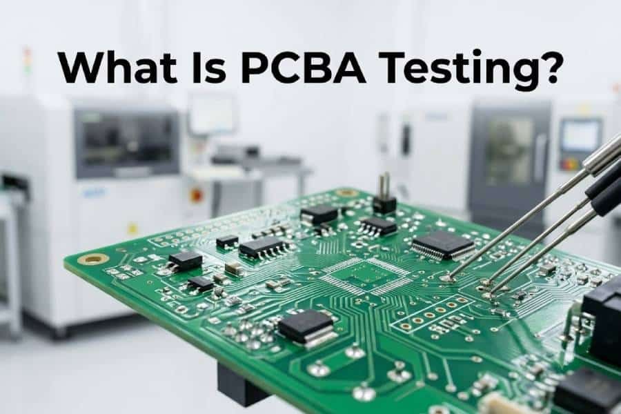
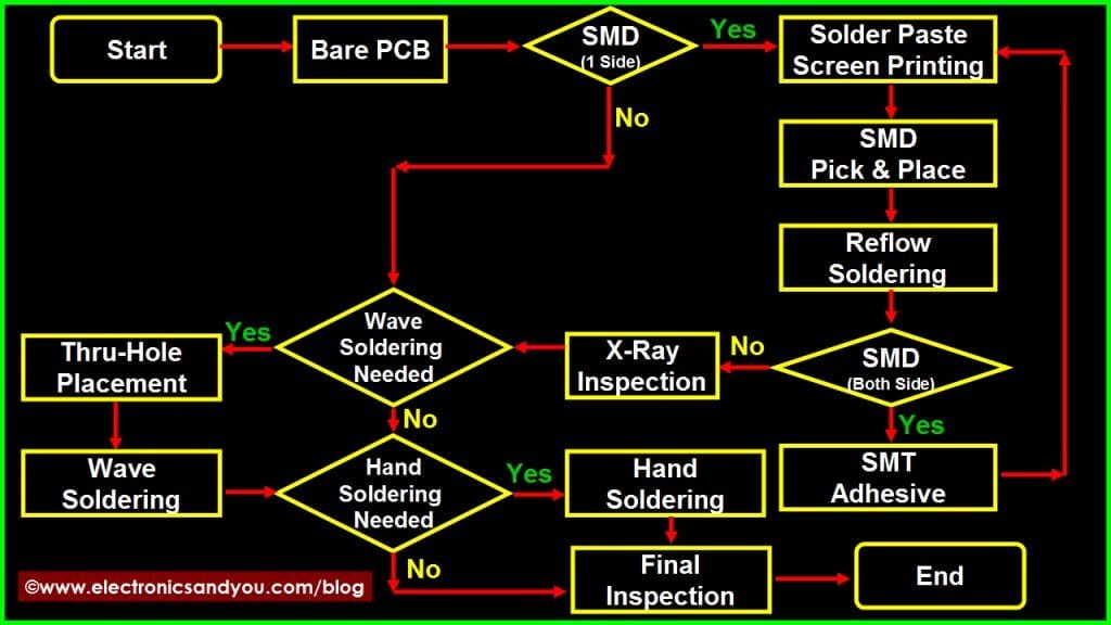
What transforms a bare green board into the “brain” of a smartphone, a medical device, or an automotive control system? That’s the job of the PCB assembly process (PCBA).
In this guide, we break down all 10 stages of PCB assembly — from the first application of solder paste to final inspection using AOI and X-ray systems. Whether you are an engineer validating a new prototype, a procurement manager sourcing high-volume production, or a business owner looking for a reliable assembly partner, understanding these steps will help you make better decisions and avoid costly manufacturing errors.
> For engineers: Focus on Steps 1–5 (stencil, paste, placement, reflow, and AOI) and Step 7 (X-ray for BGAs).
> For procurement and management: Pay special attention to Steps 8–10 (selective soldering, final inspection, and packaging), where quality control and delivery reliability are determined.
JHYPCB uses fully automated SMT lines, in-house AOI/SPI inspection, and lead-free reflow soldering to execute each of these steps with precision. By the end of this guide, you will know exactly how a professional PCB assembly house turns your design into a ready-to-use board.
Let’s start with Step 1.
Step 1: Creating the SMT Stencil

What happens:
Before any solder touches the board, we create a laser-cut stainless steel stencil that matches the exact pad layout of your PCB design. The stencil is placed over the board, with apertures (openings) positioned precisely where solder paste needs to be deposited.
Why it matters:
The stencil determines the volume and location of solder paste. If the apertures are misaligned, too large, or too small, the resulting solder joints will be weak, bridged, or missing entirely — leading to component placement failures later in the process. At JHYPCB, we use laser-cut stencils with ±0.01mm precision to ensure perfect alignment, even for fine-pitch components like 0.4mm QFPs and BGAs.
Related service: Need a custom stencil for a quick-turn prototype? Learn about our SMT stencil fabrication →

Step 2: Applying Solder Paste
What happens:
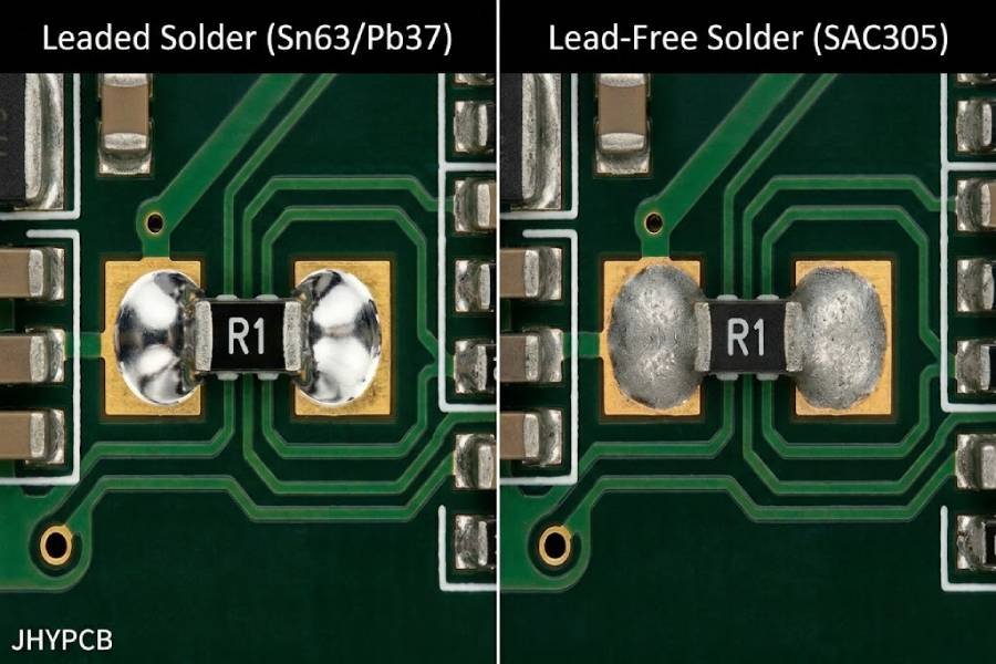
The stencil is clamped onto the PCB, and an automated screen printer applies solder paste — a gray, paste-like mixture of solder alloy (typically SAC305, lead‑free) and flux. A squeegee moves across the stencil, forcing the paste through the apertures and onto the board’s contact pads.
After printing, a 3D Solder Paste Inspection (SPI) system scans the board to verify:
- The volume of paste on each pad
- Proper alignment
- Height consistency (avoiding too much or too little paste)
Why it matters:
Solder paste application is the single most critical step for Surface Mount Technology (SMT) assembly. Too little paste results in a weak or open solder joint; too much paste can cause bridging (shorts) under fine-pitch components. The SPI check catches these issues immediately, so the process can be corrected before components are placed.
At JHYPCB, we maintain real-time SPI monitoring on our SMT lines, with statistical process control (SPC) feedback to ensure every board meets the same paste volume targets — whether you order 10 boards or 10,000.
Pro tip: For prototypes or small batches, we can also run a first-article SPI report and share it with you for approval before full production.

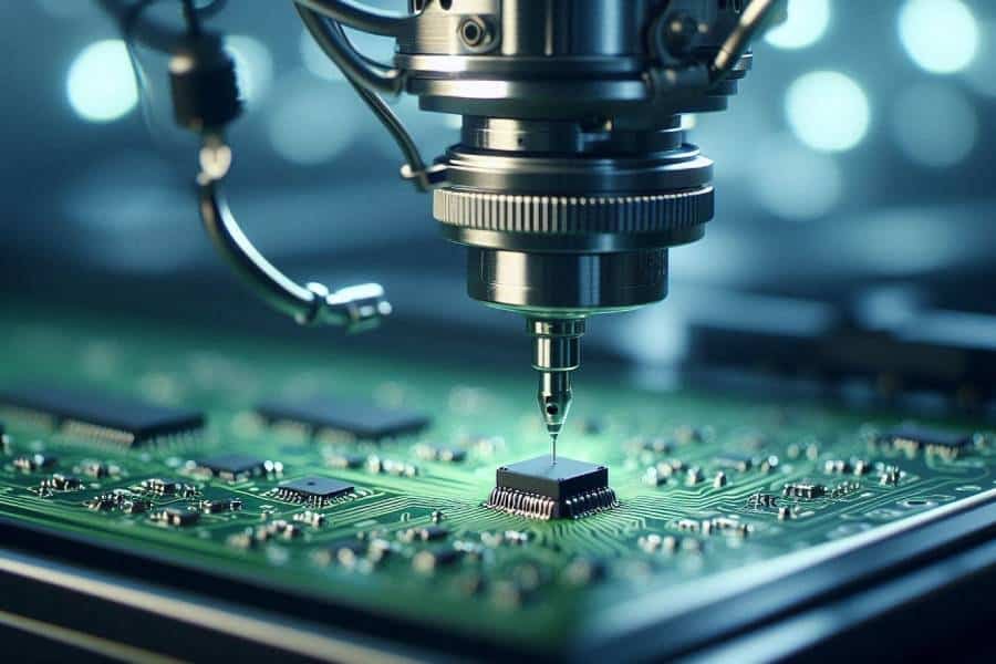
Step 3: Component Placement
What happens:
After solder paste is applied, the PCB moves to a high-speed pick-and-place machine. This machine uses vacuum nozzles to pick individual components from feeders or trays and places them onto their designated solder paste pads.
The placement coordinates are programmed directly from your PCB design files (Gerber or Centroid data). Using high-resolution cameras, the machine:
- Aligns each component to fiducial marks on the PCB
- Rotates components to the correct orientation
- Places them with typical accuracy of ±0.05mm (or ±0.025mm for fine-pitch components)
For prototypes or small batches, the same machine can be manually loaded with reels or cut-tape components. For high-volume production, the process is fully automated, placing up to 30,000 components per hour.
Why it matters:
Even a 0.1mm misalignment can cause tombstoning (a component standing on end), insufficient solder contact, or bridging after reflow. Accurate placement ensures every component sits squarely on its pads, so the reflow soldering step forms a reliable electrical and mechanical bond.
At JHYPCB, we use fiducial-backed optical alignment and real-time placement verification. For fine-pitch ICs (0.4mm or less) and BGAs, we apply extra placement pressure and vision checks to guarantee alignment before soldering.
Quality checkpoint: After placement, operators perform a first-article inspection using a magnified vision system. Learn about our quality assurance process →

Step 4: Reflow Soldering
What happens:
Once all SMT components are placed, the PCB enters a reflow oven — a precisely temperature-controlled tunnel typically 4–6 meters long. The oven contains multiple heating zones followed by cooling zones.
As the board travels through the oven, the solder paste goes through a standard reflow profile:
| Zone | Typical Temperature | Purpose |
|---|---|---|
| Preheat | 150–180°C | Activates flux, removes solvents |
| Soak (thermal equilibrium) | 180–200°C | Equalizes temperature across board |
| Reflow (peak) | 235–245°C (lead‑free) | Melts solder alloy; forms joints |
| Cooling | Below 220°C (ramp down) | Solidifies solder; prevents thermal shock |
The entire thermal profile is customized for each PCB based on factors like board thickness, copper layer count, component density, and solder paste type.
Why it matters:
The reflow profile is one of the most sensitive and quality-critical steps. If the ramp rate is too fast:
- Components or the board can crack from thermal shock
- Solder balls or splatter can form, causing shorts
If the peak temperature is too low:
- Solder doesn’t fully melt (cold joints, poor electrical connection)
If the cool-down is too fast:
- Mechanical stress can damage ceramic components or BGA solder balls
At JHYPCB, we run a KIC thermal profiler for each new PCB design before full production. This generates a real-time temperature curve, which we compare to the solder paste manufacturer’s recommended profile. Only when the profile matches perfectly do we proceed with assembly.
Pro tip: For high-reliability applications (automotive, medical, aerospace), we can provide a reflow profile report as part of your build documentation.
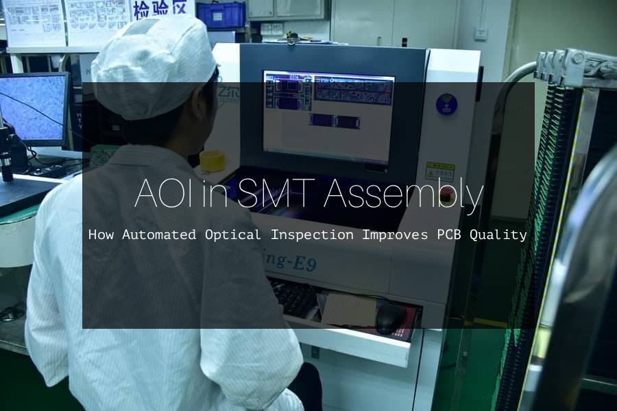
Step 5: Automated Optical Inspection (AOI)
What happens:
Immediately after reflow soldering, the PCB moves into an Automated Optical Inspection (AOI) system. AOI uses high-resolution cameras (2D or 3D) and advanced lighting to capture detailed images of the assembled board.
The system compares these images against your original CAD design files and a set of predefined “golden” standards. Within seconds, it can identify a wide range of potential defects:
Component Issues
- Missing component
- Misaligned or rotated part
- Wrong component (based on size, color, or marking)
Polarity error (diode, capacitor, or IC orientation)
Solder Joint Issues
- Solder bridging (shorts)
- Insufficient or excessive solder
- Solder balls or splatter
- Tombstoning (component standing on end)
AOI can inspect over 95% of all solder joints on a typical PCB. However, it cannot see what’s hidden underneath components like BGAs or LGAs — that’s where X-ray inspection (Step 7) comes in.
Why it matters:
AOI is the first major quality gate after soldering. It catches defects early and with high speed, preventing faulty boards from continuing to downstream processes (which would waste time and money). Defects are flagged in real time, and operators can:
- Immediately rework simple issues (e.g., resoldering a bridged joint)
- Pause the line if a repeating problem is found (e.g., misaligned feeder)
- Log data for process improvement (which feeds directly into Step 6: SPC)
At JHYPCB, we use 3D AOI systems for fine-pitch and high-density boards. 3D AOI can measure solder joint height and shape, which is far more accurate than 2D for detecting head-in-pillow defects or insufficient paste under large components.
Quality checkpoint: For critical projects, we can share AOI inspection images and reports with you as part of your build documentation.

Step 6: Statistical Process Control (SPC)
What happens:
Statistical Process Control (SPC) is not a single inspection machine — it’s a data-driven methodology that runs continuously throughout the entire assembly line. At JHYPCB, SPC software collects real-time measurements from:
| Data Source | What It Monitors |
|---|---|
| Solder Paste Printer (SPI) | Paste volume, height, alignment |
| Pick-and-Place Machine | Placement accuracy, feeder performance |
| Reflow Oven (KIC profiler) | Peak temperature, soak time, slope rates |
| AOI System | Defect types, counts, and locations by component |
The software analyzes these measurements against upper and lower control limits (UCL/LCL) that we define based on industry standards (IPC-A-610) and your specific product requirements.
When a process begins to drift — for example, the paste printer’s alignment slowly shifts by 0.01mm over a shift — SPC detects the trend before a defect occurs. The system alerts engineers, who can then recalibrate the machine proactively.
Why it matters:
SPC is the difference between reactive quality control (finding defects after they happen) and predictive quality control (preventing defects from happening in the first place). The benefits are direct and measurable:
- Higher first-pass yield: Fewer boards need rework or scrap
- Consistent quality: Each board matches the last, whether you order 100 or 100,000
- Lower cost: Correcting a drifting process costs far less than reworking a whole batch
- Full traceability: SPC logs provide proof of process control for ISO, automotive (IATF 16949), or medical (ISO 13485) compliance
At JHYPCB, we provide SPC summary reports upon request, especially for high-reliability industries. You can see exactly how each critical parameter (paste volume, placement accuracy, reflow peak temp) stayed within spec across your entire production run.
Pro tip: Ask us about setting up custom SPC control limits for your specific product — particularly if you have very tight component pitch or high-value BGAs.
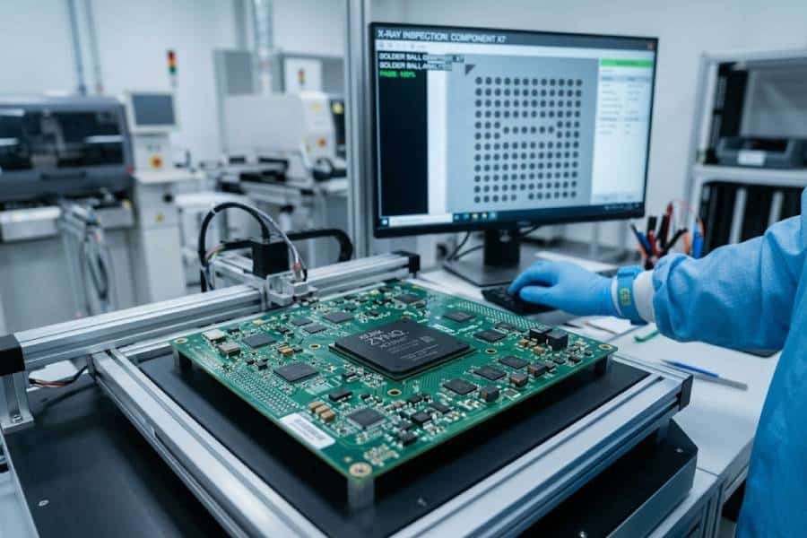
Step 7: X-Ray Inspection (AXI)
What happens:
While AOI inspects what the camera can see, Automated X-Ray Inspection (AXI) reveals what is hidden beneath components. The PCB passes through an X-ray system that uses low-energy, focused X-rays to create high-resolution images of internal solder joints and structures.
The system analyzes these images to detect defects that are invisible to optical inspection:
| Component Type | What X-Ray Reveals |
|---|---|
| BGAs (Ball Grid Arrays) | Solder ball voids, bridging, missing balls, head-in-pillow defects |
| QFNs / LGAs (leadless packages) | Solder joint wetting, shorts under the component body |
| THT through-hole joints | Incomplete or excessive solder fill inside plated holes |
| Shielded or multi-layer areas | Internal PCB structures, buried vias, or hidden shorts |
For BGAs — which are widely used in processors, memory chips, and FPGAs — X-ray is not optional if you need high reliability. A single void that exceeds 25% of the ball’s volume can lead to intermittent connections or thermal failure in the field.
AxI systems can operate in two modes:
2D X-ray – Provides a single top-down image. Fast and effective for most BGA void and bridging checks.
3D X-ray (CT scan) – Builds a full 3D model of the board. Used for complex failure analysis, prototype validation, or high-reliability samples (aerospace, medical, military).
Why it matters:
X-ray inspection closes the last remaining blind spot in SMT quality control. Without it, you are shipping boards with potentially defective BGA or LGA connections that cannot be seen or tested electrically with 100% certainty.
At JHYPCB, we perform 2D X-ray inspection on every BGA-equipped board as a standard practice. For high-reliability projects, we can offer:
- 100% X-ray of all BGAs per IPC-A-610 Class 3 standards
- X-ray reports with void percentage measurements for each ball
- 3D CT scanning for failure analysis or first-article validation
Quality guarantee: We provide X-ray images and void analysis reports upon request.

Step 8: Selective Soldering for THT Components
What happens:
Not all components can be surface mounted. Connectors, transformers, high-relay switches, and large electrolytic capacitors typically require Through-Hole Technology (THT) for mechanical strength and current-carrying capacity.
But here’s the challenge: once the PCB has already gone through reflow soldering for SMT components, you cannot run it through a wave soldering machine — the molten solder would wash away or damage the already-attached SMT parts on the bottom side.
That’s where selective soldering comes in.
The selective soldering machine uses a programmable, miniature solder wave nozzle (or a drop-jet fluxing system) to precisely target only the THT component leads that need soldering. The process happens in an inert nitrogen atmosphere, which prevents oxidation and produces bright, void-free joints.
The three-stage selective soldering process:
| Stage | Action | Purpose |
|---|---|---|
| 1. Fluxing | A small nozzle sprays flux onto the specific THT leads | Cleans surfaces, promotes solder flow |
| 2. Preheating | Localized infrared or hot gas preheats the target area | Activates flux, reduces thermal shock |
| 3. Soldering | A programmable mini-solder wave touches each lead for 1–3 seconds | Forms a reliable, filleted THT joint |
The entire process is CNC-controlled — the machine moves the PCB over the stationary solder nozzle, or moves the nozzle under the PCB, following coordinates programmed directly from your CAD files.
Why it matters:
Selective soldering solves a critical manufacturing conflict: how to build mixed-technology (SMT + THT) boards without compromising quality or efficiency.
Compared to manual soldering:
| Aspect | Manual Soldering | Selective Soldering |
|---|---|---|
| Consistency | Operator-dependent | Programmed, repeatable |
| Speed | Slow (5–10 seconds per joint) | Fast (<2 seconds per joint) |
| Quality | Risk of cold joints, bridges, or damage | Nitrogen atmosphere ensures clean joints |
| Scaling | Not practical beyond 5–10 boards | Runs 100s or 1000s identically |
| Cost | Low tooling, high labor | Higher tooling, low labor for volume |
For double-sided SMT boards (components on both sides), selective soldering is often the only viable option for adding THT components without reflowing and potentially dropping bottom-side parts.
At JHYPCB, we use inline selective soldering systems with closed-loop process control. Our typical application areas include:
- Mixed-technology PCBs for industrial controls
- Automotive modules (connectors and relays)
- Medical devices (high-reliability THT joints)
- Power supply boards (large capacitors and transformers)
Pro tip: For new designs, consider using press-fit THT connectors or surface-mount versions of traditional THT parts to avoid selective soldering altogether — but when you need it, we are fully equipped.
Step 9: Final Inspection, Cleaning, and Packaging
What happens:
After reflow soldering, AOI, X-ray inspection, and selective soldering, the PCB enters the final processing stage — where it is cleaned, visually verified one last time, and prepared for shipment.
PCB Cleaning
Soldering processes leave behind flux residues, even with no-clean solder pastes. For high-reliability applications, these residues must be removed because they can:
- Become hygroscopic (absorb moisture) and cause surface corrosion over time
- Insulate test points or interfere with conformal coating adhesion
- Attract dust in sensitive environments (medical, aerospace)
At JHYPCB, we use:
- Deionized (DI) water (never tap water) to avoid introducing conductive ions
- High-pressure spray washing with rotating jets to reach under low-clearance components
- Hot air drying in a multi-stage convection oven
The result is a chemically clean PCB that meets IPC Class 2 or Class 3 cleanliness standards.
Final Visual Inspection (FVI)
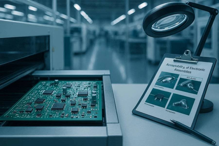
Before packaging, every board undergoes a human-aided final visual inspection under magnification:
- Operators check for any defects missed by AOI/X-ray (e.g., cosmetic issues, component orientation on very large parts)
- Solder joint fillets are verified against IPC-A-610 acceptance criteria
- Any remaining flux residues or foreign material is flagged
- Serial numbers or UID labels are verified for traceability
FVI serves as the last human quality gate before packaging. It catches the rare defect that automated systems might miss — such as a subtle crack in a connector housing or a reversed capacitor that passed polarity check due to ambiguous markings.
Packaging for Shipment
The final step is packaging the boards to survive transit and arrive in perfect condition:
| Packaging Element | Purpose |
|---|---|
| ESD-safe bags (vacuum-sealed or anti-static) | Prevents electrostatic discharge damage |
| Moisture barrier bags + desiccant + humidity indicator card | Protects against moisture absorption (critical for lead-free and MSL-sensitive components) |
| Custom-cut anti-static foam or trays | Prevents mechanical shock and component crush |
| Reinforced cartons with void fillers | Avoids box movement and corner damage during shipping |
| Packing list + COC (Certificate of Conformance) | Documents what was shipped and that it passed all inspections |
For prototype or small-batch orders, we typically use ESD-safe bags + bubble wrap + reinforced carton. For reel-to-reel or tray-fed high-volume orders, we pack in original manufacturer packaging or custom trays per your specification.
Why it matters:
The best assembly quality means nothing if boards arrive damaged, contaminated, or shorted due to ESD.
At JHYPCB, we follow IPC-J-STD-033 for moisture-sensitive device handling and ANSI/ESD S20.20 for electrostatic control. Our packaging process is documented and audited as part of our ISO 9001:2015 certification.
Pro tip: For humid environments or long-term storage, request vacuum sealing with desiccant and a humidity indicator card. We provide this as a standard option for lead-free and high-reliability PCBs.

Step 10: Functional Testing and Feedback Collection
What happens:
Step 10 is optional for some customers and mandatory for others — it depends on your product’s reliability requirements. Functional testing goes beyond solder joint inspection to verify that the entire circuit performs as designed.
Types of Functional Testing
| Test Type | What It Does | When Used |
|---|---|---|
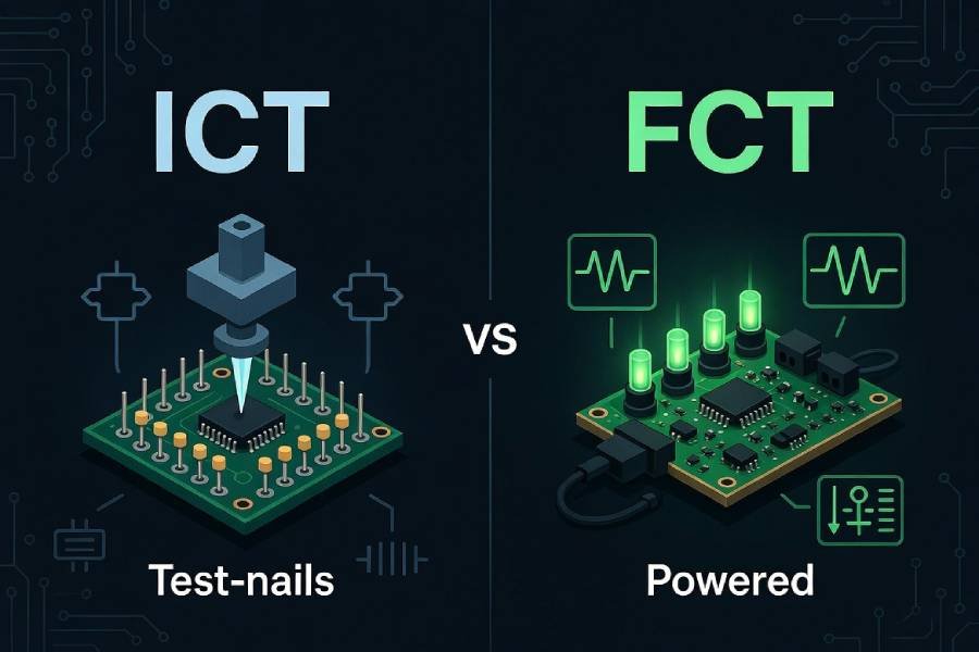
| In-Circuit Test (ICT) | Uses a bed-of-nails fixture to measure individual component values (resistance, capacitance, etc.) | High-volume production; quick verification of each component |
| Flying Probe Test | Mobile probes contact test points without a custom fixture | Prototypes, small batches, or complex boards where ICT fixture cost is prohibitive |
| Boundary Scan (JTAG) | Tests interconnections between ICs using built-in test logic | Dense digital boards with limited physical test access (e.g., BGAs) |
| Functional Test (custom) | Powers up the board and runs a custom script or fixture to simulate real operation | End-of-line testing for assembled products (e.g., power supply output, sensor reading, display function) |
At JHYPCB, we commonly perform:
- Flying probe testing for prototypes and low-volume (default for most engineering samples)
- ICT for medium-to-high volume production (tooling cost amortized over many boards)
- Custom functional testing when you provide a test fixture, script, or specification
Rework and Repair
If any test fails — or if AOI/X-ray/FVI flagged a repairable defect — the board enters a rework station:
- Defective SMT components are removed using hot-air rework stations with precision thermocouples
- THT components are desoldered using vacuum or solder wick
- New components are re-soldered (usually by hand for SMT or selective soldering machine for THT)
- The board is re-inspected (AOI, X-ray, or test as needed)
Rework is time-consuming and carries risk (thermal damage, pad lifting). That is why our SPC and AOI processes focus on preventing defects — but when rework is needed, our technicians follow IPC-7711/7721 standards.
Feedback Collection and Continuous Improvement
The final — and most overlooked — step is closing the loop between production and design.
When we collect test data, defect logs, and customer feedback, our engineering team analyzes it for root causes. Common outcomes:
| Finding | Corrective Action |
|---|---|
| Recurring solder bridging on a 0.5mm QFP | Adjust stencil aperture design; reduce paste volume |
| Repeated polarity reversal on a diode | Suggest a PCB layout change (add polarity silkcreen arrow) |
| BGA voiding above 25% consistently | Adjust reflow profile (increase soak time) |
| Customer reports intermittent field failure | Perform 3D X-ray CT; update test coverage for that failure mode |
This feedback loop is formalized in our 8D (Eight Disciplines) problem-solving process for quality incidents. For proactive customers, we can also provide a DFM (Design for Manufacturing) report after first-article inspection — free of charge — to help you optimize your design before high-volume production.
Why it matters:
Functional testing separates visually perfect boards from electronically correct boards. It is your final assurance that the product will work in the real world.
Feedback collection turns quality data into design improvements — reducing cost, lead time, and failure rates for your next order.
At JHYPCB, we offer functional testing as:
- Standard: Flying probe test for prototypes (included at no extra charge for most orders)
- Optional: ICT, boundary scan, or custom fixture-based functional test (quote based on complexity)
- Premium: First-article DFM report + 8D root cause analysis for any quality deviation
Final CTA: Your PCBA project has unique requirements. Contact our engineering team for a free design review and test plan recommendation →
Key Equipment at JHYPCB: The Machines Behind the 10 Steps
The process steps above are executed on JHYPCB‘s in-house SMT line, which includes fully automated, precision equipment from leading manufacturers. Below is a summary of the key machines we use at each stage — and how they contribute to quality.
| Equipment Type | Brand / Model (Examples) | Process Step(s) | Key Capability |
|---|---|---|---|
| Laser Stencil Cutter | LPKF / LPKF MultiCut | Step 1 | ±0.01mm aperture accuracy; fine-pitch support down to 0.3mm |
| Solder Paste Printer | DEK NeoHorizon / ASMPT | Step 2 | ±0.025mm alignment; closed-loop feedback to SPI |
| 3D SPI System | Koh Young / KY8030-3 | Step 2 (post-print) | 100% paste volume, height, and area measurement |
| High-Speed Pick-and-Place | Yamaha / YSM20 + YSM10 | Step 3 | 30,000 CPH; ±0.035mm accuracy (0.025mm for fine-pitch) |
| Reflow Oven | Heller / 1913 MK5 | Step 4 | 10 zones, nitrogen-capable, <±1°C uniformity |
| KIC Thermal Profiler | KIC / KIC Start | Step 4 (setup) | Real-time reflow profile validation vs. paste specs |
| 3D AOI System | Mirtec / MV-3L | Step 5 | 15µm resolution; detects head-in-pillow, polarity, tombstoning |
| SPC Data Platform | Custom / Yxlon (integration) | Step 6 | Real-time CPK tracking; automated alarms for drift |
| 2D / 3D X-Ray (AXI) | Yxlon / Cheetah EVO | Step 7 | 0.5µm pixel size; void % measurement; 3D CT option |
| Selective Soldering | Ersa / VERSAFLOW 4 | Step 8 | Nitrogen inerting; programmable mini-wave; 0.5s/joint cycle |
| In-Circuit Tester (ICT) | Teradyne / TestStation | Step 10 (optional) | 3000 nodes/sec; bed-of-nails or flying probe |
| Flying Probe Tester | Takaya / APT-9400 | Step 10 (standard) | 6 probes; no fixture cost; ideal for prototypes |
| Deionized Cleaning System | Kolb / WetBench DI | Step 9 | 18 MΩ·cm DI water; 400 L/min spray pressure |
Note: Equipment models are updated periodically. Contact our engineering team for current capabilities for your specific component types (e.g., 01005 passives, 0.3mm pitch BGAs, or large-format boards up to 800mm).
Why We List Our Equipment
For procurement professionals and quality engineers, knowing which specific machines will run your boards matters — because different equipment has different:
- Component limits (smallest passives, largest ICs, thickest boards)
- Process stability (CPK >1.33 is standard on above lines)
- Traceability (each machine logs data for batch-level traceability)
At JHYPCB, we maintain calibration records and maintenance logs for every machine above, audited annually as part of our ISO 9001:2015 certification. Upon request, we can provide:
- Machine capability reports (e.g., placement accuracy CPK for your specific components)
- First-article inspection data with machine-specific IDs
- Equipment validation reports for automotive or medical customers (IATF 16949 or ISO 13485 compliance)
Frequently Asked Questions (FAQs) About the PCB Assembly Process
The lead time depends on order type and quantity:
| Order Type | Typical Turnaround | Key Factors |
|---|---|---|
| Prototype (1–10 boards) | 24–48 hours (quick-turn) | Component availability, stencil fabrication |
| Small batch (11–100 boards) | 5–7 working days | SMT setup, AOI/SPI validation |
| Medium batch (101–500 boards) | 7–12 working days | Reflow profiling, first-article sign-off |
| High volume (>500 boards) | 12–20 working days | Lead time for ICs/reels, ICT fixture fabrication |
At JHYPCB, our quick-turn PCB assembly service can deliver prototypes in as little as 24 hours for simple, in-stock component designs. Request a lead time estimate for your specific BOM →
| Technology | How It Works | Best For | Typical Component Examples |
|---|---|---|---|
| SMT | Components placed on surface pads, soldered via reflow | High density, small size, automated assembly | Resistors (0201), QFP, BGA, LEDs |
| THT | Leads inserted into drilled holes, soldered (wave or selective) | Mechanical strength, high heat/stress resistance | Connectors, transformers, large capacitors |
| Mixed Technology | Both SMT and THT on the same board | Complex products requiring both density and durability | Automotive ECUs, medical monitors, power supplies |
JHYPCB supports all three types. For mixed-technology boards, we use selective soldering (Step 8) to protect SMT components while soldering THT leads.
Quality assurance for hidden joints (like BGAs, LGAs, and QFNs) relies on X-ray inspection (Step 7) . We perform:
- 2D X-ray on every BGA-equipped board as standard
- Void percentage measurement (IPC-A-610 accepts <25% void per ball)
- 3D CT scanning for failure analysis or first-article validation
All X-ray images and void reports can be shared upon request.
Yes. We offer functional testing to verify electrical performance, not just solder joint quality:
| Test Type | Best For | Fixture Cost | Test Coverage |
|---|---|---|---|
| Flying Probe | Prototypes, small batches | None (no fixture) | Component-level (R, C, L, diode, shorts) |
| In-Circuit Test (ICT) | Medium-to-high volume | $800–$3000 one-time | High (analog/digital, BSCAN) |
| Custom Functional Test | End-of-line product validation | Provided by customer | Full (actual product behavior) |
Flying probe is included at no extra charge for most prototype orders. For volume production, ICT is recommended for its speed and repeatability.
JHYPCB's facility is certified for international quality and environmental standards:
| Certification | Scope |
|---|---|
| ISO 9001:2015 | Quality management system (design, assembly, testing) |
| RoHS | Lead-free, restricted substances compliance |
| UL | UL 796 recognition for PCB manufacturing |
| IATF 16949 (on request) | Automotive quality management (available for qualified projects) |
| ISO 13485 (on request) | Medical device manufacturing (available for qualified projects) |
Our standard process complies with IPC-A-610 Class 2 (industrial/consumer). We can build to Class 3 (high-reliability) for aerospace, medical, or automotive applications upon request.
Still have a specific question about your PCB design or assembly requirements? Contact our engineering team directly →
From Bare Board to Complete Assembly: The 10 Steps in Summary
You have now walked through every stage of the PCB assembly process — from the precision of stencil creation and pick-and-place, through the hidden-world inspection of X-ray, to the final validation of functional testing.
At each step, the difference between a mediocre assembler and a great one comes down to:
- ✓ Process control (SPC prevents defects)
- ✓ Inspection depth (AOI + X-ray leaves no joint unchecked)
- ✓ Rework discipline (IPC standards, not shortcuts)
- ✓ Feedback loops (your next batch is better than the last)
At JHYPCB, we execute all 10 steps in-house, under one roof, with real-time data collection and ISO 9001:2015 certified quality systems. Whether you need a 24‑hour prototype or a 50,000‑piece production run, the same rigorous process applies.
Your next step is simple
Review your design for manufacturability
Request a free DFM report to catch issues early.
Get DFM check →Discuss complex requirements
BGA, mixed-tech, high-voltage? Talk to our engineering team.
Schedule a call →Whether you need 5 prototype boards or 50,000 production units, the same 10-step process — executed with precision — delivers reliability you can count on.
JHYPCB — Your partner for prototype, quick-turn, and high-volume PCB assembly.
PCB Assembly Process Videos
Printed Circuit Board Assembly Process
SMT PCB Assembly Process | Surface Mount Technology Manufacturing Process
PCB Assembly Factory Tour (Full) – How To Assemble A PCB