SMT PCB Assembly Process
Introduction to SMT PCB Assembly
Surface-mount technology (SMT) is the cornerstone of modern electronics manufacturing, enabling the production of compact, high-performance devices like smartphones, laptops, and IoT gadgets. The SMT PCB assembly process combines automation, precision, and efficiency to mount electronic components directly onto the surface of printed circuit boards (PCBs). Unlike traditional through-hole technology, SMT eliminates the need for drilling, resulting in smaller, lighter, and more cost-effective designs. A typical SMT production line requires only 5-7 operators and can assemble a PCB in just 30-60 seconds, making it ideal for high-volume manufacturing.
This guide provides a detailed walkthrough of the SMT PCB assembly process, covering each step from barcode printing to final inspection. Whether you’re an electronics engineer, procurement specialist, or manufacturer, you’ll gain insights into the technical nuances, best practices, and quality control measures that ensure reliable PCB assembly. By understanding these steps, you can optimize production, minimize defects, and select the ideal SMT partner for your specific needs. Ready to dive into the world of SMT? Let’s explore the process step by step.
What is SMT?
Surface-mount technology is a method for assembling electronic components directly onto the surface of printed circuit boards (PCBs). By soldering components to pads on the PCB’s surface, SMT eliminates the need to drill holes through the board, as required in traditional through-hole technology (THT). This approach enables the production of smaller, lighter, and more complex electronic devices, making SMT the preferred choice for modern electronics manufacturing.
Key Advantages of SMT
- Miniaturization: SMT supports tiny components, allowing for compact designs in products like smartphones, wearables, and medical devices.
- High Automation: SMT production lines rely on advanced machines, such as pick-and-place systems and reflow ovens, reducing labor costs and human error.
- Improved Performance: Surface-mounted components enable shorter signal paths, enhancing electrical performance and reliability.
- Cost Efficiency: Automated processes and higher component density lower production costs in high-volume manufacturing.
SMT vs. THT: A Comparison
While THT involves inserting component leads through drilled holes and soldering them on the opposite side, SMT mounts components directly on the surface. THT is still used for larger or high-power components, but SMT dominates due to its speed, precision, and compatibility with automated assembly. For example, SMT can assemble thousands of components per hour, compared to THT’s slower, manual-intensive process.
SMT’s versatility and efficiency make it indispensable for industries ranging from consumer electronics to automotive and aerospace. As technology advances, SMT continues to evolve, supporting even smaller components and more intricate PCB designs.
SMT PCB Assembly Process Steps
The SMT PCB assembly process is a highly automated sequence of steps that transforms bare PCBs into functional electronic assemblies. Each stage, from initial preparation to final inspection, is critical to ensuring quality, efficiency, and reliability. In this section, we begin with the first step: Shop Floor Tracking via Barcode Printing.
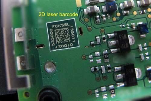
Step 1: Shop Floor Tracking: Barcode Printing
Before any assembly begins, a unique tracking barcode is printed on the bare PCB to enable real-time monitoring throughout the production process. This barcode integrates with the Shop Floor Control System (SFCS) or Shop Floor Data Collection System (SFDC), allowing manufacturers to track production status, quality metrics, and potential defects. Barcodes can be applied using three main methods:
- Label Paper: Adhesive labels with pre-printed barcodes, easy to apply but less durable.
- Inkjet Printing: Direct ink application, offering flexibility but requiring careful calibration for clarity.
- Laser Printing: Etches barcodes onto the PCB surface, providing superior durability and precision.
Modern SMT lines increasingly use two-dimensional (2D) barcodes, such as QR codes, which store more data in a smaller footprint compared to traditional one-dimensional barcodes.
Best Practices for Barcode Printing:
- Clarity and Scannability: Ensure barcodes are legible and easily read by scanners to avoid tracking errors.
- Durability: Select a printing method that withstands friction, heat, and long-term storage without fading.
- Positioning: Place barcodes in non-functional areas to avoid impacting the PCB’s aesthetics or performance.
Effective barcode implementation enhances traceability, reduces quality control issues, and streamlines production management, setting the foundation for a successful SMT assembly process.
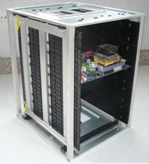
Step 2: Bare Board Loading
The bare board loading stage marks the entry of PCBs into the SMT production line. This critical step involves transferring bare PCBs—those without components—onto a conveyor belt for subsequent assembly processes. Typically, bare boards are neatly stacked in a material rack or magazine and fed into the line one by one using a mechanical device. This automated system ensures precise and efficient board handling, minimizing delays and maintaining production flow.
Two common methods are used for bare board loading:
- Material Rack Loading: Boards are stacked and separated by a mechanical arm, which places them onto the conveyor. This method is cost-effective but risks minor surface scratches during transfer.
- Magazine Loading: Boards are housed in protective magazines, reducing the chance of damage. Magazines are designed to integrate seamlessly with SMT equipment, ensuring smooth transitions.
Sensors monitor the process, sending data to a control system that dictates when to load or pause boards, optimizing throughput. Proper loading prevents misalignment and surface damage, which could compromise subsequent steps like solder paste printing.
Best Practices for Bare Board Loading:
- Use magazines for delicate or high-value PCBs to minimize scratches.
- Calibrate sensors to ensure accurate board placement on the conveyor.
- Regularly inspect racks or magazines for debris that could obstruct loading.
By prioritizing precision and board protection, bare board loading sets the stage for a seamless SMT assembly process, ensuring high-quality outcomes.
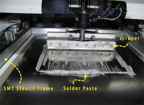
Step 3: Solder Paste Printing
Solder paste printing is a pivotal step in the SMT PCB assembly process, where solder paste—a mixture of tiny solder particles and flux—is applied to the pads of a PCB. This paste serves two critical functions: it temporarily secures electronic components during placement and forms permanent solder joints during reflow soldering. The paste is applied through a precision-engineered SMT stencil, which aligns with the PCB’s pads to deposit the correct amount of paste in the exact locations.
The quality of solder paste printing directly impacts soldering reliability. Too little paste can lead to weak joints, while excess paste may cause bridging or short circuits. Modern SMT lines use automated stencil printers equipped with vision systems to ensure precise alignment and consistent paste application.
Best Practices for Solder Paste Printing:
- Stencil Design: Use high-quality stainless steel stencils with laser-cut apertures to match pad sizes precisely.
- Paste Control: Maintain optimal paste viscosity and store it at recommended temperatures (typically 2–10°C) to prevent degradation.
- Regular Maintenance: Clean stencils after every 5–10 prints to remove residue and prevent clogging.
- Alignment Verification: Use vision systems to confirm stencil-to-PCB alignment before printing.
By optimizing solder paste printing, manufacturers can reduce defects and enhance the reliability of the final PCB assembly, laying a solid foundation for subsequent steps.
Step 4: Solder Paste Inspection (SPI)
Solder Paste Inspection (SPI) is a critical quality control step in the SMT PCB assembly process, performed immediately after solder paste printing. SPI uses advanced optical instruments to evaluate the quality of solder paste deposits on the PCB’s pads. By analyzing parameters like volume, height, area, and alignment, SPI detects issues such as insufficient paste, excess paste, or misalignment that could lead to soldering defects like weak joints or short circuits.
The SPI system employs 2D or 3D imaging technology, similar to Automated Optical Inspection (AOI), to scan the PCB surface. If defects are identified, the board can be cleaned and reprinted before proceeding to component placement, significantly reducing rework costs and scrap rates. Leading SMT manufacturers rely on SPI to ensure consistent soldering quality, especially for high-density or complex PCBs.
Best Practices for Solder Paste Inspection:
- Use 3D SPI Systems: 3D imaging provides more accurate measurements of paste volume and height compared to 2D systems.
- Set Strict Tolerances: Define acceptable paste parameters to catch defects early without excessive false positives.
- Regular Calibration: Calibrate SPI equipment regularly to maintain accuracy and reliability.
- Act on Findings: Remove defective boards for cleaning or adjust printing parameters to prevent recurring issues.
By catching solder paste issues early, SPI enhances the reliability of the SMT assembly process, minimizing defects and ensuring high-quality solder joints.
-In-The-SMT-Assembly-Process.jpg)
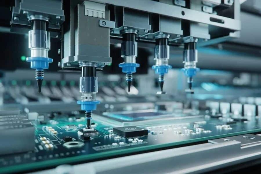
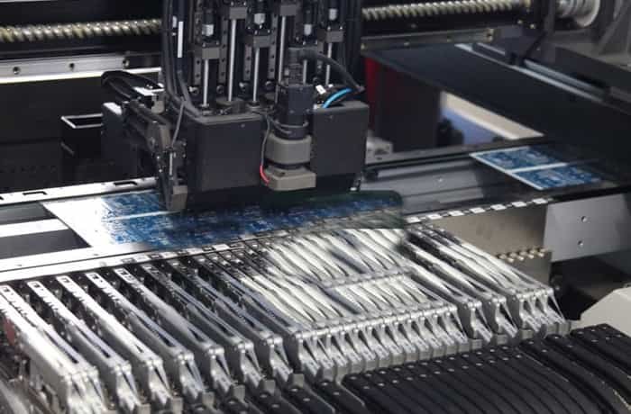
Step 5: High-Speed Chip Placement
High-speed chip placement is a cornerstone of the SMT PCB assembly process, where small passive components—such as resistors, capacitors, and inductors—are precisely positioned onto the PCB’s solder paste-covered pads. These components, often referred to as “small chips,” typically have only two terminals, requiring high positional accuracy to ensure reliable soldering. High-speed placement machines, equipped with multiple nozzle heads, can place thousands of components per hour, making them ideal for high-volume production.
The machine’s nozzles pick components from tape-and-reel feeders and place them onto the PCB, guided by precise vision systems and software. The sticky solder paste, applied in the previous step, holds the components in place during rapid board movement, preventing misalignment. A typical SMT line may include one to four high-speed placement machines to optimize throughput.
Best Practices for High-Speed Chip Placement:
- Calibrate Vision Systems: Ensure accurate component alignment by regularly calibrating the machine’s cameras.
- Monitor Solder Paste Quality: Verify paste stickiness to prevent components from shifting during placement.
- Optimize Feeder Setup: Arrange tape-and-reel feeders to minimize nozzle travel time and maximize efficiency.
- Regular Maintenance: Clean nozzles and check for wear to avoid pickup errors or placement defects.
High-speed chip placement enhances production efficiency while maintaining precision, paving the way for subsequent steps in the SMT assembly process.
Step 6: General Pick and Place
General pick and place, often referred to as “slow machine” placement, is a critical step in the SMT PCB assembly process for handling larger, heavier, or multi-pin components, such as Ball Grid Arrays (BGAs), connectors, card readers, and shielding cans. Unlike high-speed chip placement machines, which prioritize speed for small passive components, general pick and place machines focus on precision and flexibility. These machines use advanced vision systems to capture images of components, adjust their position and angle, and place them accurately on the PCB’s solder paste-covered pads.
Components in this stage may come in various packaging formats, such as trays or tubes, rather than tape-and-reel. Some irregularly shaped components require custom nozzles or flat tape to enable suction by the machine’s nozzles. The slower speed ensures precise alignment, which is crucial for complex components with multiple pins or tight tolerances.
Best Practices for General Pick and Place:
- Use Vision-Guided Alignment: Calibrate cameras to ensure accurate positioning and angle adjustment for multi-pin components.
- Customize Nozzles: Employ specialized nozzles for non-standard components to ensure reliable pickup and placement.
- Verify Component Packaging: Ensure trays or tubes are compatible with the machine to avoid feeding errors.
- Monitor Placement Accuracy: Regularly inspect placed components to prevent misalignment or offset issues.
By prioritizing precision, general pick and place ensures reliable placement of complex components, enhancing the overall quality of the SMT assembly process.
Step 7: Pre-Reflow Inspection, Visual or AOI
Pre-reflow inspection is a vital quality control step in the SMT PCB assembly process, conducted after component placement but before reflow soldering. This stage ensures that components are correctly positioned and free from defects like misalignment, missing parts, or incorrect polarity. Inspection can be performed manually (visual inspection) or using Automated Optical Inspection (AOI) systems, which employ high-resolution cameras to scan the PCB surface and detect anomalies with precision.
AOI is particularly valuable for high-density PCBs, as it quickly identifies issues that could lead to soldering defects, reducing the need for costly rework after reflow. However, certain components, such as shielding cans, may obstruct AOI’s view, necessitating complementary visual checks. For boards requiring manual placement of large or through-hole components, this step also serves as an opportunity to add these parts before soldering.
Best Practices for Pre-Reflow Inspection:
- Combine AOI and Visual Checks: Use AOI for speed and accuracy, supplemented by visual inspection for areas obscured from optical systems.
- Calibrate AOI Systems: Ensure cameras and software are regularly updated to minimize false positives and detect subtle defects.
- Train Inspectors: Equip visual inspection teams with templates or guides to ensure consistency and accuracy.
- Address Obstructions: Adjust board designs or inspection processes to account for components like shielding cans that block AOI visibility.
Effective pre-reflow inspection enhances soldering quality and reduces post-reflow rework, ensuring a robust SMT assembly process.

Step 8: Reflow Soldering
Reflow soldering is a critical stage in the SMT PCB assembly process, where solder paste melts to form strong, permanent bonds between electronic components and the PCB. This process occurs in a reflow oven, which subjects the PCB to a carefully controlled temperature profile consisting of four zones: pre-heat, soak, reflow, and cooling. The pre-heat zone gradually raises the board’s temperature, the soak zone activates the flux in the solder paste, the reflow zone melts the paste to form intermetallic compounds (IMCs), and the cooling zone solidifies the joints.
For lead-free solder paste, such as SAC305, the reflow oven must reach a minimum temperature of 217°C to melt the paste, but should not exceed 250°C to avoid damaging sensitive components. Precise temperature control is essential to prevent defects like tombstoning, solder bridging, or component deformation.
Best Practices for Reflow Soldering:
- Optimize Temperature Profile: Adjust pre-heat, soak, reflow, and cooling zones based on the solder paste’s specifications (e.g., SAC305’s 217°C melting point).
- Monitor Oven Conditions: Regularly calibrate the reflow oven to maintain consistent temperatures and avoid hot spots.
- Use Nitrogen Atmosphere: For high-reliability PCBs, a nitrogen environment reduces oxidation and improves solder joint quality.
- Inspect Post-Reflow: Check for defects like voids or incomplete joints immediately after cooling to address issues early.
Effective reflow soldering ensures durable, high-quality solder joints, completing the core assembly of the PCB.

Step 9: Post-Reflow AOI
Post-reflow Automated Optical Inspection (AOI) is a crucial quality assurance step in the SMT PCB assembly process, performed after reflow soldering to evaluate the quality of solder joints and component placement. Using high-resolution cameras and sophisticated software, AOI systems scan the PCB to detect defects such as tombstoning, solder bridging, missing components, misalignment, or incorrect polarity. This step is essential for high-density PCBs, where manual inspection may be impractical due to component size and complexity.
While AOI is highly effective, it has limitations. It cannot inspect solder joints hidden beneath components, such as those in Ball Grid Arrays (BGAs), or detect issues like false soldering or component functionality. Shadow effects near tall components can also reduce accuracy. For these reasons, AOI is often complemented by In-Circuit Testing (ICT) or Functional Verification Testing (FVT) for comprehensive quality control.
Best Practices for Post-Reflow AOI:
- Optimize Lighting and Angles: Adjust AOI camera settings to minimize shadow effects and improve defect detection.
- Combine with Other Tests: Use AOI alongside ICT or FVT to address blind spots, such as hidden solder joints.
- Regular Software Updates: Keep AOI algorithms current to reduce false positives and enhance accuracy.
- Inspect Critical Areas: Focus on high-risk components like QFNs or connectors to ensure reliable performance.
Post-reflow AOI enhances quality control, catching defects early to reduce rework and ensure reliable PCB assemblies.
Step 10: Unloading
Unloading is the final step in the core SMT PCB assembly process, where fully assembled PCBs are removed from the production line and placed into protective magazines for storage or further processing. After passing through reflow soldering and post-reflow inspections, the PCBs are transported via conveyor belts to an automated unloading system. These systems use mechanical arms or vacuum grippers to carefully transfer the boards into magazines, ensuring no damage to the delicate solder joints or components.
Magazines are designed to securely hold multiple PCBs, protecting them from physical stress and environmental factors like dust or static discharge. The unloading process is fully automated in modern SMT lines, with sensors ensuring precise placement and minimizing handling errors. Proper unloading is critical to maintaining the quality of the assembled PCBs before they proceed to visual inspection or additional testing.
Best Practices for Unloading:
- Use Compatible Magazines: Ensure magazines match the PCB size and SMT equipment specifications to prevent misalignment or damage.
- Minimize Handling: Rely on automation to reduce manual contact, preserving solder joint integrity.
- Monitor Environmental Conditions: Control humidity and static levels to protect sensitive components during unloading.
- Inspect Magazines: Regularly clean and check magazines for debris or wear to avoid scratching or contaminating PCBs.
Effective unloading ensures the assembled PCBs remain intact and ready for subsequent quality checks or packaging, concluding the SMT assembly process with high reliability.
Step 11: Visual Inspection
Visual inspection is a key quality control step in the SMT PCB assembly process, typically performed after unloading to verify the quality of assembled PCBs. This manual inspection complements Automated Optical Inspection (AOI) by addressing defects that AOI may miss, such as subtle solder joint issues, component polarity errors, or defects in areas obscured by components like shielding cans. Trained inspectors use magnifying tools and standardized templates to ensure consistency and accuracy.
While AOI excels at detecting obvious defects like tombstoning or misalignment, visual inspection is critical for high-reliability PCBs where human judgment can identify nuances that automated systems overlook. For example, inspectors may check for solder joint uniformity or verify the orientation of critical components. This step helps reduce the risk of defective boards reaching end-users, enhancing overall product reliability.
Best Practices for Visual Inspection:
- Use Inspection Templates: Provide inspectors with clear guides or templates to standardize checks for weldability and component placement.
- Train Inspectors Thoroughly: Ensure staff are skilled in identifying subtle defects, such as micro-cracks or incorrect polarity.
- Optimize Lighting: Use adequate, adjustable lighting to improve visibility of solder joints and component details.
- Supplement with AOI: Combine visual inspection with AOI to minimize false positives and cover all potential defect areas.
By integrating visual inspection into the SMT process, manufacturers ensure high-quality PCB assemblies, catching defects that automated systems may miss.

Step 12: Touch-Up or Wave Soldering
Touch-up or wave soldering is the final step in the SMT PCB assembly process for components that cannot be processed by standard SMT equipment, such as through-hole (THT) parts or larger components unsuitable for reflow soldering. Touch-up involves manual soldering using a soldering iron and solder wire to correct minor defects or attach specific components. Wave soldering, on the other hand, passes the PCB over a molten solder wave to bond THT components efficiently in high-volume production.
Manual touch-up requires precision to avoid overheating components or damaging solder joints. The soldering iron’s tip, maintained at a controlled temperature (typically 300–350°C), melts the solder wire to form reliable joints. Wave soldering is automated but generates more heat, necessitating careful PCB design to protect SMT components. Both processes produce fumes containing harmful heavy metals, requiring robust fume extraction systems to ensure operator safety.
Best Practices for Touch-Up or Wave Soldering:
- Control Soldering Temperature: Use precise temperature settings to prevent damage to components or PCB pads during touch-up.
- Ensure Fume Extraction: Install effective ventilation systems to protect workers from toxic soldering fumes.
- Optimize Wave Soldering Parameters: Adjust wave height and conveyor speed to achieve uniform solder joints without excess solder.
- Post-Soldering Inspection: Check for defects like cold joints or solder bridges to ensure quality after touch-up or wave soldering.
By carefully executing touch-up or wave soldering, manufacturers ensure complete and reliable PCB assemblies, addressing components outside the standard SMT process.

Common SMT Issues and Solutions
In the SMT PCB assembly process, even with advanced automation and rigorous quality controls, issues can arise that affect the quality and reliability of the final product. Identifying and addressing these challenges promptly is essential to minimize defects, reduce rework costs, and ensure high-performance PCBs. Below, we outline the most common SMT issues and their practical solutions to help manufacturers optimize their processes.
1 Poor Solder Paste Printing
Issue: Inconsistent or insufficient solder paste application can lead to weak solder joints, while excess paste may cause solder bridging or short circuits.
Solution:
- Optimize stencil design with precise aperture sizes to match PCB pads.
- Regularly clean stencils (every 5–10 prints) to prevent residue buildup.
- Use Solder Paste Inspection (SPI) to detect and correct printing defects before component placement.
2 Component Misalignment
Issue: Components may shift during high-speed placement or reflow, leading to misalignment or poor electrical connections.
Solution:
- Calibrate pick-and-place machines to ensure accurate component positioning.
- Verify solder paste stickiness to secure components during placement.
- Adjust reflow oven temperature profiles to prevent excessive vibration or thermal shock.
3 Solder Joint Defects
Issue: Defects like tombstoning, solder balls, or cold joints can compromise PCB reliability.
Solution:
- Fine-tune reflow temperature profiles to ensure proper solder melting and solidification (e.g., SAC305 at 217°C minimum).
- Use nitrogen atmospheres in reflow ovens to reduce oxidation and improve joint quality.
- Conduct post-reflow AOI and visual inspections to identify and address defects early.
4 Component Damage
Issue: Sensitive components may be damaged due to excessive heat, static discharge, or improper handling.
Solution:
- Maintain reflow oven temperatures below 250°C to protect delicate components.
- Implement electrostatic discharge (ESD) protection measures during handling and unloading.
- Use magazines for unloading to minimize manual contact and physical stress.
By proactively addressing these common SMT issues, manufacturers can enhance production efficiency, reduce waste, and deliver reliable PCBs for demanding applications.
Advantages and Future Trends of SMT
Surface-mount technology (SMT) has revolutionized electronics manufacturing, offering unparalleled advantages over traditional methods like through-hole technology (THT). Its ability to support compact, high-performance, and cost-effective PCB assemblies makes it indispensable across industries. This chapter explores SMT’s key benefits and emerging trends shaping its future.
Advantages of SMT
- Miniaturization: SMT enables the use of tiny components, facilitating compact designs for devices like smartphones, wearables, and IoT modules.
- High Automation: Advanced machines, such as pick-and-place systems and reflow ovens, streamline production, reducing labor costs and human error.
- Enhanced Performance: Shorter signal paths in SMT assemblies improve electrical performance, supporting high-speed and high-frequency applications.
- Cost Efficiency: Higher component density and automated processes lower manufacturing costs, especially for high-volume production.
These advantages make SMT the preferred choice for consumer electronics, automotive, medical, and aerospace applications, delivering reliable and innovative solutions.
Future Trends in SMT
As technology evolves, SMT continues to advance, driven by demands for smaller, smarter, and more sustainable electronics. Key trends include:
- AI-Driven Quality Control: Artificial intelligence is enhancing Automated Optical Inspection (AOI) and Solder Paste Inspection (SPI), improving defect detection accuracy.
- Micro-Miniaturization: Support for ultra-small components, like 0201 metric chips, enables even denser PCB designs.
- Smart Manufacturing: Integration of Industry 4.0 technologies, such as IoT and real-time data analytics, optimizes SMT production lines for efficiency and traceability.
- Sustainable Processes: Eco-friendly solder pastes and energy-efficient reflow ovens are reducing the environmental impact of SMT manufacturing.
These trends promise to make SMT faster, more precise, and environmentally responsible, ensuring its dominance in the future of electronics assembly.
FAQs
To further clarify the SMT PCB assembly process, we’ve compiled answers to some frequently asked questions. These insights address common concerns and help you better understand surface-mount technology (SMT) and its applications.
What is the difference between SMT and THT?
Surface-mount technology (SMT) mounts components directly onto the PCB surface, enabling smaller, automated, and high-density designs. Through-hole technology (THT) involves inserting component leads through drilled holes and soldering them on the opposite side, suitable for larger or high-power components. SMT offers faster production and miniaturization, while THT provides stronger mechanical bonds for specific applications.
Why is solder paste inspection (SPI) important in SMT?
Solder paste inspection (SPI) verifies the quality of solder paste deposits before component placement. By detecting issues like insufficient or excess paste, SPI prevents soldering defects, reducing rework costs and improving reliability, especially for complex PCBs.
How can I choose a reliable SMT factory?
Look for factories with advanced equipment (e.g., 3D SPI, AOI, high-speed pick-and-place machines), robust quality control processes, and a proven track record. Certifications like ISO 9001 and IPC standards are also indicators of reliability. Contact pcbelec.com for expert SMT services tailored to your needs.
What are common defects in SMT assembly, and how are they addressed?
Common defects include solder bridging, tombstoning, and component misalignment. These can be mitigated by optimizing solder paste printing, calibrating placement machines, and fine-tuning reflow temperature profiles. Regular AOI and visual inspections catch defects early for correction.
What is the future of SMT technology?
SMT is evolving with AI-driven quality control, support for ultra-small components (e.g., 0201 chips), and smart manufacturing via Industry 4.0. Sustainable practices, like eco-friendly solder pastes, are also gaining traction, ensuring SMT remains at the forefront of electronics manufacturing.
Conclusion
The SMT PCB assembly process is a cornerstone of modern electronics manufacturing, enabling the production of compact, reliable, and high-performance devices through a series of precise, automated steps. From barcode printing and bare board loading to reflow soldering and final inspections, each stage—solder paste printing, component placement, AOI, and touch-up soldering—plays a critical role in ensuring quality and efficiency. By addressing common issues like poor solder paste application or component misalignment with proactive solutions, manufacturers can minimize defects and deliver robust PCBs.
SMT’s advantages, including miniaturization, automation, and cost efficiency, make it indispensable for industries like consumer electronics, automotive, and medical devices. As the technology evolves with AI-driven quality control and sustainable practices, SMT will continue to shape the future of PCB manufacturing. For reliable SMT assembly services tailored to your needs, visit pcbelec.com to explore our capabilities, request a quote, or consult with our experts. Start optimizing your PCB production today!
Related Reading
- Laser Cut vs. Etching Stencils for SMT Assembly: Which is Best?
- One-Stop Solution: The Advantages of Turnkey PCB Manufacturing and Assembly
- Demystifying THT PCB Assembly: A Comprehensive Guide
- The Main PCB Assembly Process Steps
- How to clean the solder paste on SMT stencil?
- What is the Bill of Materials(BOM) and how to create one?
- The Production Process and Specifications of PCB SMT stencil
- What is the difference between SMT and SMD?
- Reflow Soldering VS. Wave Soldering: What’s the difference?
- How to Use PCB Stencil-Step by Step Guideline
- Optimized SMT Reflow Soldering Temperature Curves: Warm-Up vs. Gradual Heating
- What Is Prototype PCB Assembly?
- How to Get a Quote and Order PCB Assembly?