Table of Contents
Why You Need a Clear Process for Gold Finger PCBs
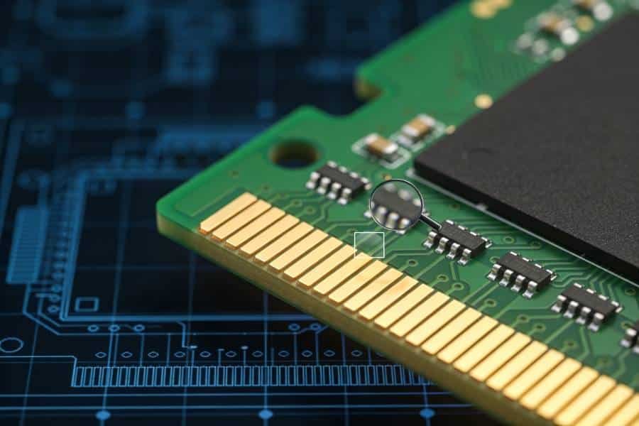
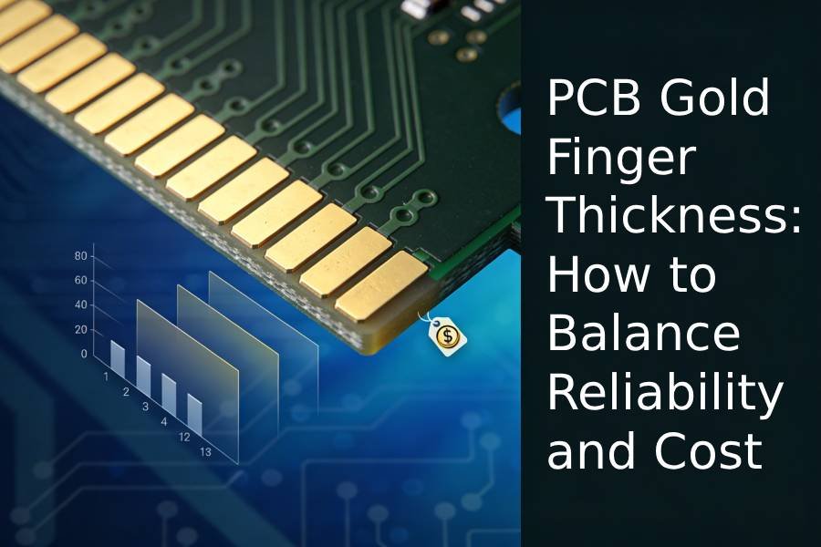
Gold finger PCBs look simple on the surface—a row of shiny edge contacts that slide into a connector—but they combine some of the most sensitive design and manufacturing details on the board. Compared with standard pads and vias, gold fingers must withstand repeated insertion, maintain low and stable contact resistance, and survive mechanical wear without cracking or peeling. That means small mistakes in layout, beveling, plating thickness, or even panelization can quickly turn into intermittent field failures that are hard to diagnose and expensive to fix.
This step‑by‑step guide walks you through the entire process of a gold finger PCB, from defining application requirements and translating them into design rules, to panelization, plating, beveling, inspection, and assembly. At each stage, we will highlight the decisions that most strongly affect reliability, cost, and lead time, so you can design edge connectors that are robust without being over‑engineered. If you are already planning a design with edge connectors, you can refer to our “Gold Finger PCB Fabrication & Manufacturing Service” while reading this guide to see what capabilities and design limits your manufacturer can support.
Step 1 – Define Application & Requirements
Before you draw a single gold finger in your PCB CAD tool, you need a clear picture of how the connector will be used over the life of the product. This first step is about turning vague statements like “plugged in sometimes” or “industrial environment” into explicit requirements that can drive your design rules and finish choices.
1.1 Mating cycles and usage pattern
Start by estimating how many times the board will be inserted and removed from its connector slot. Typical ranges include:
- Prototypes, fixtures, or one‑time installations: a handful to a few dozen cycles.
- Field‑replaceable cards in industrial or telecom systems: tens to hundreds of cycles.
- High‑cycle test interfaces or development backplanes: hundreds to thousands of cycles.
Higher mating‑cycle targets generally push you toward hard gold on the fingers with a thicker, well‑controlled plating stack, while low‑cycle applications may tolerate thinner plating or different finish combinations. It is important to document whether the cycles are concentrated during development and production testing, or spread out across years of field service, because this affects both wear and corrosion exposure.
1.2 Environment and reliability level
Next, define the environment in which the connector will operate. Key factors include:
- Temperature range and thermal cycling
- Presence of dust, humidity, corrosive gases, or vibration
- Whether insertion happens in clean ESD‑safe labs or in harsh field conditions
Gold fingers used in clean, controlled environments with low insertion forces can tolerate a narrower process window than those used in dusty factory floors or outdoor telecom cabinets. For high‑reliability domains such as medical, automotive, or communication infrastructure, you will usually align your expectations with relevant IPC and industry standards for plating quality, bevel geometry, and inspection.
1.3 Electrical role of the edge connector
Clarify what signals and power levels actually pass through the gold fingers. For example:
- Are they carrying only low‑speed control signals?
- Do they include high‑speed differential pairs that are sensitive to impedance discontinuities?
- Are there significant power rails that must make and break under load?
The more critical the signals, the more attention you must pay to finger length, spacing, stack‑up around the edge, and any keep‑out rules that affect impedance control. Power fingers may require wider pads, staggered lengths for make‑before‑break behavior, or reinforced mechanical support near the edge to avoid cracking under insertion force.
1.4 Compliance, standards, and connector constraints
Finally, align your requirements with any external constraints:
- Mechanical outline and contact pitch dictated by the mating connector
- Required bevel angle or edge thickness from the connector datasheet
- Applicable standards (IPC‑6012 / IPC‑A‑600, industry‑specific specs) that define acceptability criteria for plating, beveling, and defects
At this stage, it is also a good time to talk to your PCB manufacturer and confirm their typical hard‑gold thickness range, available bevel angles (often 30°–45°), and panelization preferences for gold finger boards. Capturing these points in a short requirement summary will make the later design and CAM review much smoother and reduce back‑and‑forth during quoting.
Step 2 – Gold Finger Design Rules at the PCB Level
Once you have clear application requirements, the next step is to translate them into concrete PCB‑level design rules for the gold finger area. Getting these details right in your CAD tool will make manufacturing smoother and greatly reduce the risk of CAM changes or quality issues later.
2.1 Finger location, length, and alignment
Gold fingers must be placed on the board edge that mates with the connector, with the outline shaped so that insertion is smooth and not obstructed by neighboring features. Ensure that all fingers are aligned in a straight line and extend far enough into the connector to achieve full overlap with the contact beams, but not so far that they risk bending or mechanical interference.
As a rule of thumb, maintain a consistent length across fingers that carry related signals (for example, differential pairs and buses) to avoid unnecessary timing skew. If you are unsure about minimum or typical finger lengths for your connector pitch and thickness, you can consult both the connector datasheet and your manufacturer’s “Gold Finger PCB fabrication guidelines” for recommended dimensions.
2.2 Keep‑out areas around the fingers
A well‑defined keep‑out region around the gold finger area is essential for both manufacturability and reliability. Common rules include:
- No plated through‑holes or vias within about 1.0 mm of the fingers
- No SMT pads or copper features too close to the beveled edge
- No silkscreen or legend printing on top of the fingers or their immediate surroundings
These constraints prevent issues such as copper exposure during chamfering, solder mask slivers, or partial plating coverage at the edge. Your fabrication notes should make it clear that the gold finger area is a dedicated contact region, not a place for test points, vias, or mounting holes.
2.3 Solder mask and surface finish definition
Gold fingers must be free of solder mask so that the nickel and gold plating can directly cover the copper contact area. In your CAD tool, that means defining a solder mask opening (window) that fully exposes each finger and extends cleanly to the board edge without narrow mask bridges.
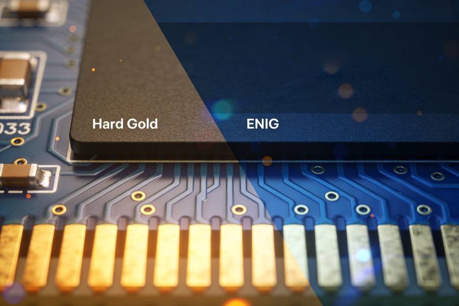
For the surface finish, explicitly distinguish between the gold finger contacts and the rest of the board. A common approach is to specify hard gold over nickel on the fingers and ENIG, HASL, or another finish on component pads, which you can implement via separate surface‑finish notes in your fabrication drawing or by referencing your manufacturer’s “Gold Finger PCB Manufacturing Service” capabilities.
2.4 Copper, stack‑up, and routing near the edge
Pay attention to the copper layout and stack‑up in and around the gold finger region. Best practices include:
- Avoid copper pours on the outer layer within the finger region so that each contact remains clearly separated and easy to insert.
- Maintain sufficient distance between internal copper planes and the board edge to prevent copper from being exposed during beveling.
- Use 45‑degree bends or arcs rather than sharp 90‑degree corners when routing into the finger pads, especially for high‑speed signals.
For high‑speed interfaces, coordinate the edge‑connector routing with your stack‑up and impedance targets so that the transition into the fingers is as smooth as possible. Short stubs, uncontrolled reference plane changes, or abrupt neck‑downs at the edge can all degrade signal integrity, even if the plating itself is perfect.
2.5 Bevel clearance and board thickness constraints
Finally, reserve enough clearance between the gold fingers and the final board outline to allow for beveling. Many manufacturers recommend at least about 0.6–1.0 mm between the end of the finger pads and the mechanical edge before chamfering, depending on board thickness and bevel angle.
If the fingers are too close to the edge, the beveling process can cut into the copper or gold, leading to weak or incomplete contacts. Typical production constraints also include minimum board thickness (often ≥ 1.2 mm) and minimum finger length for automated chamfering, so it is worth confirming these limits early with your PCB house rather than discovering them at the CAM stage.
Step 3 – Panelization & Bevel Planning for Gold Finger Boards
Panelization and bevel planning are often where a “theoretically correct” gold finger design runs into real‑world manufacturing limits. Thinking about how your boards will be arrayed, routed, and chamfered at the panel level helps avoid last‑minute CAM changes or compromised bevel quality.
3.1 Orient gold fingers consistently on the panel
Most fabricators prefer all gold fingers in a panel to face the same direction so they can pass the panel through plating and beveling equipment in a single, consistent orientation. As you create your panel drawing, orient each board so that the gold finger edge lines up along one side of the panel rather than pointing inwards randomly.
For some processes, especially when using automated beveling machines, manufacturers may also request that the gold finger edge be located on the panel perimeter instead of buried in the middle of the array. If you are not sure what your vendor can support, check their edge‑connector panelization notes or contact them through the “Gold Finger PCB Fabrication & Manufacturing Service” page before finalizing the panel layout.
3.2 Respect minimum size and spacing for beveling
Beveling requires a certain amount of mechanical access and board length along the gold finger edge. Common guidelines include:
- A minimum gold finger edge length (often around 30–40 mm) so the board can be held securely during chamfering.
- A minimum distance from the fingers to the final outline (commonly 0.6–1.0 mm) to avoid cutting into the plated area.
- A minimum board thickness (for example ≥ 1.2 mm) so the beveled edge remains structurally sound.
If your design uses very small boards or narrow modules with gold fingers, you may need to bevel the edge at the individual‑board stage and then perform a second routing step to release the outline from the panel. These extra operations can affect both cost and lead time, so it is important to confirm feasibility early with your PCB supplier.
3.3 Choose an appropriate bevel angle and document it
The bevel angle directly influences how easily the board inserts into the connector and how much material is removed at the edge. Common production angles are 30° and 45°, with 30° being a popular default that balances mechanical strength and insertion smoothness.
Your fabrication drawing should explicitly state the required bevel (for example, “Bevel gold finger edge 30°, both sides, after hard gold plating”), instead of assuming the manufacturer will guess the right value. When in doubt, follow the connector datasheet and verify that your chosen PCB house can meet that angle consistently as part of their “Gold Finger PCB manufacturing” capability.
3.4 Panel break‑off features and nearby tooling
Avoid placing break‑off tabs, mouse‑bites, or V‑cuts too close to the gold finger edge. Mechanical stress during depanelization can propagate into the connector area, potentially cracking plating or micro‑fracturing the laminate near the fingers.
Instead, position break‑off features on the opposite board edges or along non‑critical sides wherever possible. If the design forces you to place rails close to the gold fingers, leave enough clearance so that routing and beveling tools can operate freely without colliding with tab remnants or burrs.
3.5 Fiducials and registration for accurate beveling
Good registration between the panel and the beveling machine helps keep the chamfer angle and depth consistent across all boards. Adding global panel fiducials and, where needed, local fiducials near the gold finger edge can improve positional accuracy during both plating and beveling steps.
This is particularly important when fingers have tight length tolerances, staggered “make‑before‑break” profiles, or high‑speed signal integrity requirements at the edge. Sharing your panel Gerbers and bevel notes as part of an early DFM review with your fabricator will let them flag alignment or tooling risks before production starts.
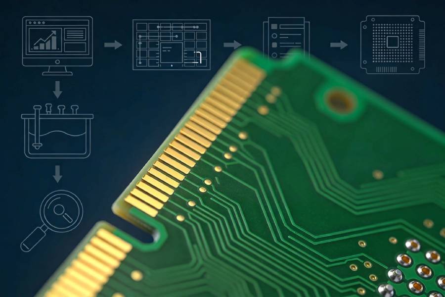
Step 4 – Manufacturing Flow: From Bare PCB to Plated Gold Fingers
Once the design, panelization, and bevel planning are in place, the gold finger PCB moves through a manufacturing flow that is similar to a standard board but with some critical extra steps for nickel and hard‑gold plating. Understanding this sequence helps you see where your design notes and finish call‑outs actually take effect on the shop floor.
4.1 Core PCB fabrication up to solder mask
The process starts with standard PCB fabrication: material cutting, inner‑layer imaging and etching, lamination, drilling, copper deposition, outer‑layer imaging, pattern plating, and outer‑layer etching. After these steps, the copper traces and pads—including the future gold finger pads at the edge—are fully defined, and the board passes through solder mask coating and imaging while excluding the finger area so that those contacts remain exposed copper.
At this point, most of the PCB surface is ready for its final finish (such as ENIG, HASL, or OSP), but the gold finger region is intentionally left bare to receive its dedicated plating stack. This separation in the flow is what allows manufacturers to combine hard‑gold fingers with different finishes on the rest of the board.
4.2 Surface preparation and nickel plating on the fingers
Before any nickel or gold is applied, the exposed copper finger pads undergo thorough surface preparation. Cleaning typically uses alkaline solutions or light micro‑etching to remove oxides, fingerprints, and residues, followed by deionized water rinses to leave a fresh, active copper surface.
The next step is electrolytic nickel plating on the finger pads. Nickel acts as a barrier layer to prevent copper diffusion into the gold and provides mechanical support for the hard‑gold layer above. Typical nickel thickness for edge connectors is on the order of a few micrometers, controlled by bath chemistry and plating time to ensure uniform coverage across the entire connector length.
4.3 Hard gold electroplating on the edge contacts
With the nickel in place, the board (or panel) goes into an electrolytic gold bath to deposit hard gold only on the finger pads. To make this possible, manufacturers use plating bars or tie‑bars that connect all the finger pads electrically along the panel edge; these bars are routed off later once plating is complete.
Hard gold for edge connectors is usually an alloy (for example, gold with cobalt) that offers much better wear resistance than pure soft gold. The plating time, current density, and bath composition are carefully controlled to achieve the specified thickness range—commonly from a few to several tens of microinches depending on the mating‑cycle requirement. After plating, the boards are rinsed and dried, and any temporary masking used to protect non‑finger areas is removed.
4.4 Applying the surface finish to the rest of the board
Once the gold fingers are plated, the rest of the PCB can receive its chosen surface finish. For many designs, this is ENIG, HASL, OSP, or another solderable finish applied to component pads and exposed copper areas outside the finger region.
Because the gold finger area has already been treated with nickel and hard gold, it is usually kept isolated from subsequent finish processes through careful masking and process sequencing. This separation ensures that the connector contacts maintain their wear‑optimized hard‑gold surface, while solder joints elsewhere on the board benefit from finishes tuned for assembly.
4.5 Beveling, cleaning, and final inspection of the fingers
After plating and surface finishes are complete, the panel goes through mechanical routing and beveling of the gold finger edge. A precision chamfering tool removes material at the specified angle (often 30° or 45°) to create a smooth, tapered edge that mates cleanly with the connector without scraping off the plated layers.
The plated fingers and beveled edge are then cleaned and inspected. Common checks include visual inspection for scratches and voids, tape tests for adhesion, thickness measurements using non‑destructive X‑ray or similar instruments, and electrical testing of the final PCB. Only after these steps are complete is the panel fully routed or depanelized into individual boards and packed for shipment.
Step 5 – Beveling, Inspection & Testing of Gold Fingers
After plating, the quality of the bevel and the plated surface determines how well the gold fingers will actually perform in real connectors. A structured beveling, inspection, and testing flow helps ensure that thickness, adhesion, geometry, and cleanliness all meet your reliability targets.
5.1 Controlled beveling and edge quality
Beveling is typically performed after hard‑gold plating using a dedicated chamfering tool set to the specified angle (commonly 30° or 45°). The goal is to create a smooth, tapered edge that guides the board into the connector without chipping the laminate or scraping away the plated layers.
After beveling, operators or automated systems check the edge for burrs, roughness, or exposed base metal. Any irregularities are removed through light deburring or rework; boards with deep damage, missing plating, or gross bevel errors are typically scrapped rather than allowed into production.
5.2 Visual inspection under magnification
Visual inspection under a microscope or magnifying lens is the first line of quality control for gold fingers. Inspectors look for a uniform gold appearance, absence of nickel “bleed‑through”, and clean, smooth surfaces along the entire contact length.
Common reject conditions include scratches, pits, discoloration, exposed copper or nickel, excess plating lumps, and contamination from solder, flux, or mask. Standards such as IPC‑A‑600 provide acceptance criteria for surface defects and cosmetic issues, especially for higher‑class boards where connector reliability is critical.
5.3 Thickness and uniformity measurement
Plating thickness and uniformity are usually verified using non‑destructive methods such as X‑ray fluorescence (XRF) sampling across multiple fingers and boards. Measurements confirm that both nickel and gold layers fall within the specified ranges for the application—for example, roughly 30–50 microinches of hard gold for high‑cycle edge connectors.
Inadequate thickness can lead to premature wear and increased contact resistance, while excessive thickness may introduce stress and risk of cracking if the process is not well controlled. Uniformity across the connector is just as important as absolute value, since thin spots or local defects tend to fail first under repeated insertion.
5.4 Adhesion checks (tape test and beyond)
Adhesion between the gold, nickel, and underlying copper is commonly checked with a tape test, as recommended in IPC guidelines. In this test, a strip of adhesive tape is pressed firmly onto the gold fingers and then peeled off; the tape is examined for any transferred plating that would indicate poor adhesion.
Some manufacturers supplement tape tests with bend or thermal‑shock testing on sample coupons to see whether plating delaminates under mechanical or thermal stress. Boards that fail adhesion tests are rejected, since flaking or peeling contacts are unacceptable in any production environment.
5.5 Functional and wear testing (when required)
For high‑reliability or high‑cycle applications, manufacturers may perform functional or wear testing on representative samples. This can include repeated insertion and removal of the test board into a mating connector, with periodic checks of contact resistance and visual inspection for wear tracks.
In some cases, signal‑integrity or power‑cycling tests are also conducted to ensure that the gold fingers maintain performance under real operating conditions. While not every production lot receives full wear testing, having this capability at either the OEM or fabricator level provides valuable data for validating plating thickness and process stability.
Step 6 – Assembly & Handling Considerations for Gold Finger PCBs
Even a perfectly plated and beveled gold finger can be damaged later during assembly, test, or field handling. Setting clear handling rules and assembly precautions helps preserve the contact surface until the board is finally installed in its connector.
6.1 Keep gold fingers clean and uncontaminated
Gold fingers should never be touched directly with bare hands or contaminated tools, because oils, flux residues, and dust can all increase contact resistance or attract corrosion over time. During assembly and test, ask operators to handle boards by their edges away from the connector side, and use gloves or finger cots when manual handling is unavoidable.
Avoid placing temporary labels, tape, or stickers over the gold finger area. Adhesive residues can be difficult to remove completely and may leave films that interfere with the wiping action of the connector contacts.
6.2 Avoid soldering or rework near the finger edge
Gold fingers are designed as mechanical contact surfaces, not as soldering points. Reflow soldering, hand soldering, or rework operations near the finger edge can splash solder or flux onto the contacts, or thermally stress the plating stack.
If you must mount components close to the edge connector, respect the keep‑out distances defined in the design phase and enforce them in assembly documentation. Any solder or flux contamination that reaches the fingers should be carefully cleaned using appropriate solvents and controlled processes, followed by inspection to confirm that no residue remains.
6.3 ESD, packaging, and shipping protection
Treat gold finger PCBs as ESD‑sensitive assemblies throughout the assembly and logistics chain. Use ESD‑safe bags, trays, or magazines that support the board without scraping the connector edge, and avoid stacking boards so that one board’s fingers can rub against another surface.
For shipping, choose packaging that immobilizes the boards and shields the gold fingers from mechanical shock and vibration. Foam inserts, slot‑style plastic rails, or dedicated edge‑connector holders can prevent the beveled edge from chipping during transport.
6.4 Handling during test and integration
In system test and integration labs, repeated insertion and removal of prototype boards can easily exceed the mating‑cycle assumptions used for production design. Where possible, use dedicated test fixtures or extender cards to take the brunt of repeated plugging, and reserve the production connector for final verification and field use.
Train technicians to inspect the gold fingers periodically for visible wear tracks, scratches, or contamination. If issues are found, it is better to replace or clean test boards early than to carry marginal contacts into final system builds.
6.5 Field replacement and service guidelines
For products designed with field‑replaceable cards, provide clear instructions in service manuals about how to insert and remove boards. This includes recommending a straight, controlled insertion motion, avoiding rocking or twisting the board, and ensuring that the connector is fully aligned before applying force.
You can also define recommended maximum mating cycles for service personnel, based on the plating thickness and connector specification. When those limits are reached in critical systems, swapping the board or connector proactively is often cheaper than troubleshooting intermittent contact problems later.
Cost and Lead Time Considerations Along the Process
Gold finger PCBs are inherently more expensive than standard boards because they add precious‑metal plating, extra processing steps, and tighter inspection requirements. Understanding where cost and lead time are generated along the process lets you decide where to invest and where to simplify.
Gold thickness vs. cost and lifetime
Gold thickness on the fingers is one of the dominant cost drivers. Thin layers used in low‑end, low‑cycle applications may add only a few percent to the PCB price, whereas thick hard‑gold layers for high‑reliability connectors can increase costs by 10–20% or more, due to both material and plating time.
Rather than defaulting to the thickest possible gold, it is better to match thickness to the real mating‑cycle requirement, using standards and manufacturer guidance as a reference. If your board only needs around a hundred insertions over its life, specifying a very heavy gold layer may offer little benefit relative to the extra cost.
Selective plating and finish combinations
Selective hard‑gold plating on just the finger area is a key strategy for controlling cost. By limiting gold to the edge contacts and using more economical finishes (ENIG, HASL, OSP) on the rest of the board, you can significantly reduce total gold usage while still meeting wear requirements.
However, selective plating introduces additional masking, panelization, and handling steps, which must be accounted for in both pricing and lead time. Clear documentation in your fabrication notes—stating exactly where hard gold is required and what finish applies elsewhere—helps avoid CAM ambiguity that can delay quoting and production.
Panel utilization and process complexity
Panel utilization also has a direct impact on cost. If gold finger boards are panelized inefficiently—because of inconsistent orientation, beveling constraints, or large keep‑out zones—the number of boards per panel drops, and the per‑board cost rises.
Similarly, extra process steps such as special beveling operations, double‑sided edge connectors, or unusually tight thickness tolerances all add time and complexity at the factory. When possible, aligning your design with “standard” options that your manufacturer already supports for their Gold Finger PCB fabrication service is an effective way to keep both cost and lead time under control.
Lead time impact of hard gold and inspection
Hard‑gold plating, selective masking, and detailed inspection all add cycle time compared with a standard PCB run. Additional steps like XRF thickness measurement, adhesion testing, and more detailed visual inspection can be essential for quality, but they also mean that gold finger boards may not fit into the fastest prototype service tiers.
If your project is schedule‑critical, discuss gold thickness, inspection level, and any “nice‑to‑have” options with your fabricator when requesting a quote. In many cases, a slightly relaxed specification (for example, moderate instead of very heavy gold, or standard instead of enhanced inspection) can shorten lead times without compromising actual field performance.
How JHYPCB Supports Your Gold Finger PCB Projects
Designing and manufacturing a gold finger PCB is much easier when your fabricator’s capabilities and process match the step‑by‑step flow described in this guide. JHYPCB focuses on edge‑connector applications with hard gold plating and precision beveling, so we can translate your requirements into concrete manufacturable parameters instead of generic notes like “gold fingers here”.
When you send your Gerber files and basic application information, our engineering team reviews not only the usual stack‑up and clearances, but also the specific gold finger details: finger length and pitch, solder mask openings, keep‑out zones, panel orientation, and bevel geometry. If we see risks—such as fingers too close to the outline for proper chamfering, unclear finish separation between fingers and pads, or ambiguous gold thickness notes—we will highlight them during DFM so they can be corrected before production.
On the process side, we run gold finger PCBs through a controlled sequence of nickel plating, hard‑gold electroplating, masking for other finishes, precision beveling, and targeted inspection. This includes verifying plating thickness with X‑ray or similar methods on sample boards, checking bevel angle and edge quality, and performing adhesion and visual inspections against IPC‑style criteria for connector contacts.
If you are planning a new design and want to align your layout with real manufacturing limits from the start, you can share your concept and prelim Gerbers through our “Gold Finger PCB Fabrication & Manufacturing Service” page and request a focused review on the edge connector section. For engineers who already have a frozen design, we can quote prototypes and small‑batch builds with hard gold thickness and inspection levels tailored to the mating cycles, environment, and cost targets you defined in the earlier steps of this guide.
Conclusion
From the first application requirements to final beveling and inspection, a gold finger PCB goes through many more decisions and process steps than a standard board. If you treat these as a structured flow—defining mating cycles and environment, applying solid design rules, planning panelization and bevels, and aligning plating, inspection, and handling with your targets—you greatly reduce the risk of intermittent connector problems later in the field.
The practical takeaway for engineers is that you do not need to over‑specify everything to be “safe”, but you do need to be explicit where it matters: gold thickness, bevel angle, finish separation between fingers and pads, and basic handling rules. Working with a manufacturer that understands this end‑to‑end process lets you focus on the system design while they handle the details of plating, beveling, and quality control.
If you are ready to move from theory to an actual build, you can share your files and requirements through our “Gold Finger PCB Fabrication & Manufacturing Service” page and request a quote along with a focused DFM review on the edge connector area. Tell us your expected mating cycles, environment, and any relevant standards, and we will recommend suitable gold thickness, bevel geometry, and finish combinations, then turn that into prototypes or small‑batch production with clear lead times and pricing.