Table of Contents
Why Gold Fingers Show Up in So Many Systems
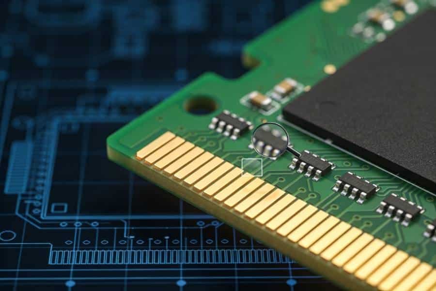
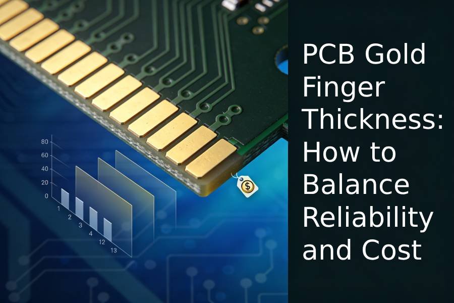
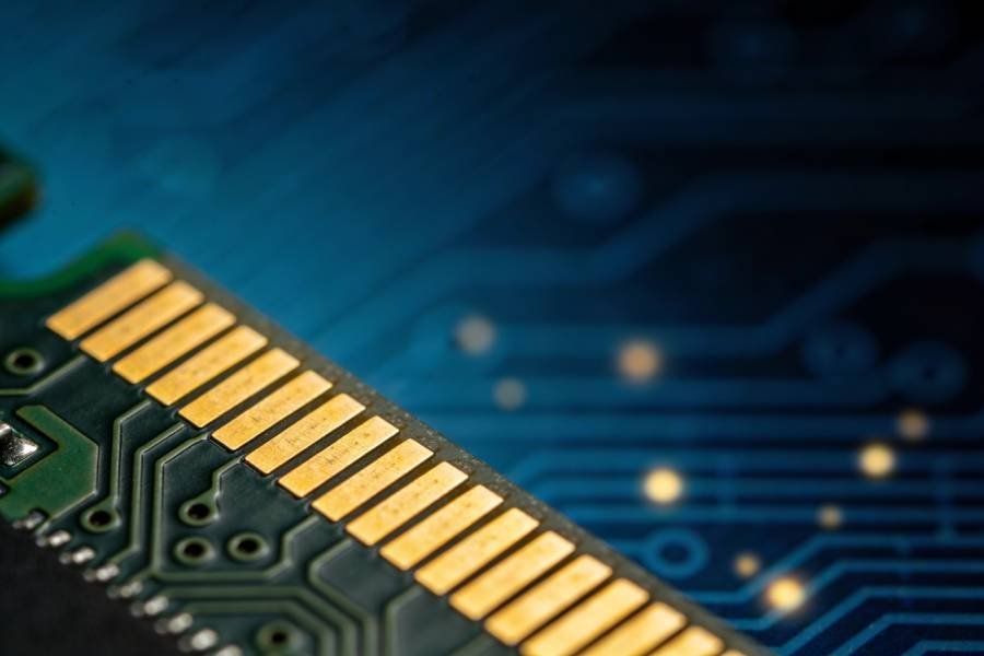
Gold fingers are one of those PCB features that you notice only when they fail: the shiny edge contacts that quietly handle high‑speed signals, power, and repeated insertion cycles across a wide range of products. From desktop PCs and servers to switches, base stations, and industrial control racks, these edge connectors turn circuit boards into swappable modules and interface cards.
What all of these applications have in common is the need for stable, low‑resistance connections that survive both environmental stress and mechanical wear. That is where gold’s corrosion resistance, hardness, and consistent contact properties make a difference, especially when combined with a well‑designed connector and controlled plating process. In this article, we will look at typical use cases of PCB gold fingers in computers, networking, and industrial control, and highlight the practical requirements they impose on design and manufacturing. If you are planning such a design, you can compare these examples with your own project while reviewing our “Gold Finger PCB Fabrication & Manufacturing Service” capabilities to see what finishes, bevels, and panel options your manufacturer can support.
Typical Applications in Computers and Data Centers
1. Memory modules and storage add‑in cards
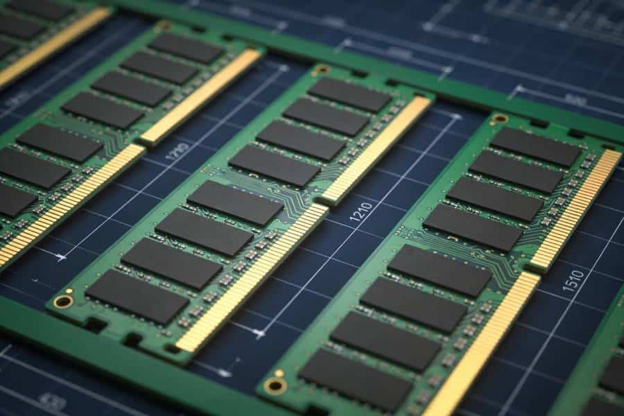
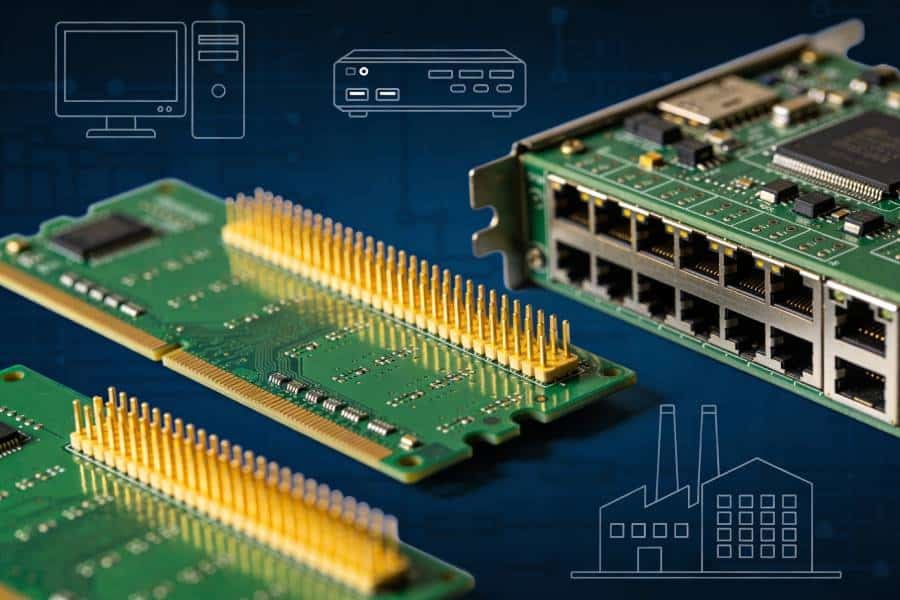
One of the most visible uses of PCB gold fingers is on memory modules such as DDR4/DDR5 DIMMs and SODIMMs. These boards plug into edge connectors on the motherboard or server backplane and may see hundreds of insertion cycles during development, upgrades, and service. Gold‑plated fingers provide the wear resistance and low contact resistance needed to maintain multi‑gigabit data rates over the life of the system.
A similar pattern appears on storage‑related add‑in cards. PCIe SSDs, RAID controllers, and other storage adapters use gold fingers to interface with motherboard or backplane slots, combining high‑speed data lanes with power and control signals along the same edge connector. Here, consistent plating thickness and clean bevels help prevent intermittent faults that could otherwise show up as data errors or unexplained device drops.
2. Graphics cards and PCIe expansion boards
Discrete graphics cards (GPUs) and other PCIe expansion boards—such as network interface cards, sound cards, capture cards, and specialized accelerator cards—also rely on gold fingers. These boards plug into PCIe slots on the motherboard, where the connector must carry high‑bandwidth differential pairs, reference clocks, control lines, and power, all through a compact edge interface.
In workstations and servers, expansion cards may be swapped or reseated during upgrades and maintenance, adding mating cycles on top of the electrical stress. Hard‑gold‑plated fingers with appropriate thickness help maintain stable contact resistance and signal integrity across those cycles, which is why PCIe and similar edge connectors are classic use cases for gold fingers rather than cheaper finishes.
3. Backplanes, riser cards, and mezzanine modules in servers
Data‑center and enterprise systems often use backplane architectures, where multiple server blades, line cards, or storage modules plug into a common board through edge connectors. In these designs, both the plug‑in cards and sometimes the backplane itself carry gold fingers to support dense, high‑speed interconnects under continuous operation.
Riser cards and mezzanine modules are another common form factor. For example, low‑profile servers may use riser cards with gold fingers to fan out PCIe lanes to horizontally mounted expansion boards, or employ mezzanine cards with edge connectors to add networking or accelerator functions on top of a baseboard. In all of these cases, gold fingers enable modular, field‑serviceable designs without sacrificing bandwidth or reliability.
Gold Fingers in Networking and Telecom Equipment
1. Line cards and interface modules in switches and routers
In carrier‑grade and enterprise switches and routers, many of the main functions are implemented on plug‑in line cards and interface modules. These cards slide into a chassis backplane or midplane using edge connectors with rows of gold fingers to carry data, control, and power between the module and the common fabric.
Such line cards are designed for field replacement and upgrades, so the edge connectors are expected to endure frequent insertion and removal under less‑than‑perfect conditions. Hard‑gold‑plated fingers with controlled thickness and bevel geometry help maintain reliable contact despite vibration, temperature changes, and occasional contamination in telecom environments.
2. Network interface cards and modular transceiver bays
Networking equipment also uses gold fingers in more compact roles, such as NICs and mezzanine networking modules inside servers or network appliances. These boards connect via edge connectors to host PCBs, providing Ethernet, Fibre Channel, or other link types through a modular card form factor.
In addition, many systems expose external transceiver bays (for example SFP/SFP+, QSFP, and similar modules) on a front panel, while the internal analog and digital paths terminate on plug‑in PCBs or adapter cards. Gold fingers on those internal boards support high‑speed differential pairs and power lines that must remain stable across temperature cycles and repeated service events.
3. Base stations, RRUs, and outdoor networking hardware
Wireless base stations, remote radio units (RRUs), and outdoor networking hardware often combine harsh environmental conditions with modular architecture. Plug‑in RF front‑end modules, control boards, or power distribution cards use gold finger edge connectors to connect into a shared backplane or motherboard inside sealed enclosures.
Here, gold fingers must tolerate not only insertion cycles but also exposure to humidity, temperature extremes, and potential contamination during installation or service. Hard‑gold finishes paired with appropriate beveling and strict keep‑outs around the connector edge help maintain low, stable contact resistance in these demanding environments. When you design networking or telecom cards that fit these patterns, you can refer to our “Gold Finger PCB Fabrication & Manufacturing Service” for guidance on suitable gold thickness, bevel angles, and panelization options for such applications.
Industrial Control and Automation Use Cases
1. PLC backplanes and modular I/O cards
Programmable logic controllers (PLCs) are a classic example of modular industrial control systems built around backplanes and plug‑in I/O cards. Each I/O card—digital input/output, analog input, temperature, motion control, and so on—uses gold finger edge connectors to mate with the PLC rack, carrying both field signals and internal power and communication buses.
These cards are often inserted and removed in factory environments with dust, vibration, and temperature variation, sometimes while the rest of the system remains powered. Hard‑gold fingers with appropriate thickness, beveling, and strict keep‑outs help ensure that connector contacts remain stable despite repeated maintenance operations and long service life.
2. Industrial PCs, expansion cards, and custom backplanes
Industrial PCs and embedded controllers also make heavy use of gold fingers, both in standard formats (such as PCIe expansion cards) and in custom backplane systems. For example, ruggedized industrial computers may use card‑edge connectors for CPU modules, communication cards, and specialized interface boards that must be easily replaceable without disturbing the rest of the system.
In many cases, these connectors must handle higher shock and vibration levels than office IT equipment. Gold fingers with robust plating and carefully controlled board thickness and bevel geometry help maintain consistent contact pressure and minimize fretting or micro‑motion wear in such environments.
3. Field devices, instrumentation, and test fixtures
Beyond centralized controllers, gold fingers also appear on field devices and instrumentation modules that need to plug into carrier boards or docking stations. Examples include modular sensor heads that plug into a base unit, portable data acquisition modules with edge connectors, and calibration or programming fixtures designed for repeated insertion of device PCBs.
Test fixtures are a particularly demanding application because they can see thousands of mating cycles during product development and production test. In these cases, hard‑gold‑plated fingers on both the DUT (device under test) boards and the fixture’s interface cards are chosen specifically for their wear resistance and stable contact resistance under frequent use. If you are designing industrial or test hardware that fits these patterns, you can align your connector layout and plating requirements with our “Gold Finger PCB Fabrication & Manufacturing Service” to ensure the edge fingers are built for the expected cycle count and environment.
What These Applications Have in Common (Technical Requirements)
Across computers, networking, and industrial control, most gold finger applications share a similar set of technical requirements that drive both design and manufacturing choices. At a high level, these connectors must combine stable electrical performance with mechanical robustness and predictable manufacturability over many years of operation.
1. Stable contact resistance over many mating cycles
In all three domains, gold fingers carry signals and power that cannot tolerate intermittent contact. Whether it is a PCIe GPU, a switch line card, or a PLC I/O module, the connector must maintain low, stable contact resistance over dozens, hundreds, or even thousands of insertion and removal cycles.
That requirement points directly to hard‑gold plating with sufficient thickness over a nickel underlayer, combined with a controlled bevel and clean, mask‑free contact surfaces. Designs that underestimate mating cycles or environmental stress tend to see early wear, fretting, or oxidation‑related issues at the connector.
2. High‑speed signal integrity and low noise
Computers, networking gear, and modern industrial systems all push high‑speed serial links and sensitive control signals through their edge connectors. Gold finger regions therefore need controlled‑impedance routing, continuous reference planes, and careful assignment of differential pairs and ground or shield fingers.
Crosstalk and reflections are common risks if fingers are packed too tightly or routed without regard for pair spacing and return paths. In practice, that means treating the gold finger section as part of the high‑speed channel, not just as a mechanical interface, and coordinating layout with connector and stack‑up specifications.
3. Mechanical robustness and environmental tolerance
From data centers to factory floors and outdoor telecom cabinets, gold finger connectors must cope with vibration, shock, temperature cycling, and varying levels of contamination. The edge connector structure—board thickness, bevel angle, finger geometry, and keep‑outs—has to be robust enough to avoid cracking, chipping, or delamination under these conditions.
This is why most real‑world designs avoid placing vias, sharp routing, or fragile mechanical features near the connector edge, and why beveling and panelization choices are so important. Done correctly, these measures help keep the plated contacts mechanically supported and clean throughout the product’s service life.
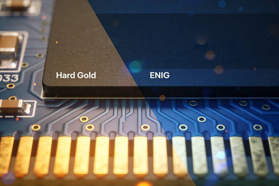
4. Clear plating, bevel, and inspection specifications
Finally, all of these applications depend on clear, testable specifications for plating, beveling, and inspection. Typical requirements include defined gold type (hard gold vs ENIG), thickness ranges, bevel angle and length, acceptable cosmetic and dimensional tolerances, and targeted inspection of the connector edge during fabrication.
Without this level of clarity, different builds or suppliers may interpret “gold fingers” differently, leading to inconsistent performance across batches. Working with a manufacturer that offers a dedicated Gold Finger PCB fabrication & manufacturing service makes it easier to turn these common requirements into a repeatable process, with documented design rules and DFM checks aligned to these application needs.
How JHYPCB Supports Gold‑Finger‑Heavy Designs
Designs that make heavy use of gold fingers—whether in computers, networking gear, or industrial control—place higher demands on both PCB layout and fabrication than ordinary boards. JHYPCB focuses on these edge‑connector applications by combining hard‑gold capability, controlled beveling, and panelization know‑how with early DFM feedback tailored to gold finger regions.
When you submit Gerbers and requirements, our engineering team does more than a generic manufacturability check. We review the edge connector area specifically: gold thickness and finish combination, bevel angle and clearance to the pads, keep‑outs around the fingers, inner‑layer copper pull‑backs, and panelization choices that affect plating and depanelization near the connector edge.
On the process side, JHYPCB’s Gold Finger PCB Fabrication & Manufacturing Service supports nickel plus hard‑gold plating on the fingers, typical thickness ranges suited to different mating‑cycle targets, and 30°–45° bevels with controlled depth and edge quality. Panels are set up with appropriate plating buses, routing and tab strategies, and inspection steps (including visual checks and thickness verification on the connector edge) to keep performance consistent across builds.
If you are designing GPUs, PCIe cards, switch line cards, PLC modules, or test fixtures that rely heavily on edge connectors, you can share a short application description along with your files through our “Gold Finger PCB Fabrication & Manufacturing Service” page and request a gold‑finger‑focused DFM review. Based on your expected mating cycles, environment, and interface speeds, we can recommend suitable gold thickness, bevel geometry, and panelization strategies, then turn them into prototypes or small‑batch production with predictable cost and lead times.
Conclusion
From PCs and servers to switches, base stations, and PLC racks, the same simple pattern repeats: gold fingers turn bare PCBs into plug‑in modules that can be swapped, upgraded, and serviced without rewiring the entire system. Once you recognize these typical applications, it becomes easier to set realistic requirements for mating cycles, signal integrity, and environmental robustness instead of treating every edge connector the same.
For most engineers, the practical challenge is less about knowing that gold fingers exist and more about translating “this is a GPU card” or “this is a PLC I/O module” into concrete specifications for plating thickness, bevel angle, keep‑outs, and inspection. Working with a fabricator that understands these application patterns and has a defined process for hard‑gold edge connectors helps ensure that your next computer, networking, or industrial control design behaves like the real‑world examples in this article—not like a one‑off experiment.
If you are planning a new design that relies heavily on edge connectors, you can send your files and a short description of the application through our “Gold Finger PCB Fabrication & Manufacturing Service” page and request a focused DFM review on the gold finger area. Tell us whether your board looks more like a PCIe card, a switch line card, or a PLC module, and we will help you choose suitable gold thickness, bevel geometry, and panelization options, then turn that into manufacturable prototypes or small‑batch builds with clear cost and lead‑time expectations.