Table of Contents
Introduction
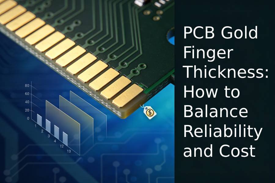
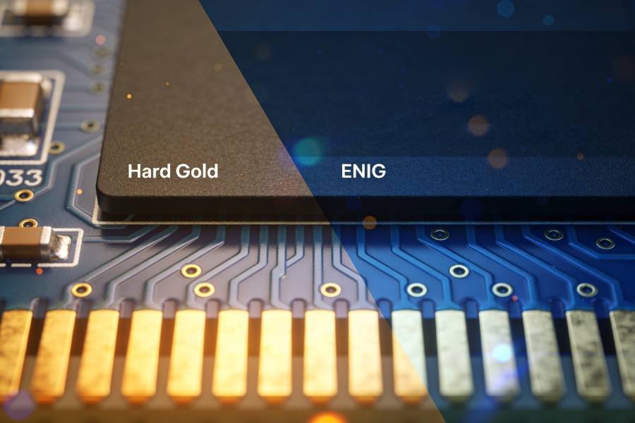
When you design a PCB with edge connectors, one of the first questions that comes up is whether the gold fingers should use hard gold or ENIG. Both finishes contain gold and both can meet IPC requirements, but they behave very differently when it comes to wear resistance, solderability, process cost and long‑term reliability. Choosing the wrong finish can lead to premature connector wear, unexpected contact problems or unnecessary cost added to every board you build.
Hard gold plating is traditionally associated with high‑cycle edge connectors and keypads, while ENIG is the workhorse finish for solderable pads and fine‑pitch components across the rest of the PCB. In practice, many designs end up mixing the two, using hard gold only on the fingers and ENIG elsewhere to balance performance and price. In this article, we will look at how ENIG and hard gold are applied, compare their strengths and weaknesses specifically for PCB gold fingers and provide practical guidelines to help you choose the right finish for your next edge‑connector design.
If you are already planning a design with edge connectors, you can refer to our “Gold Finger PCB manufacturing capabilities” while reading this guide.
How ENIG and Hard Gold Plating Work
ENIG process in brief
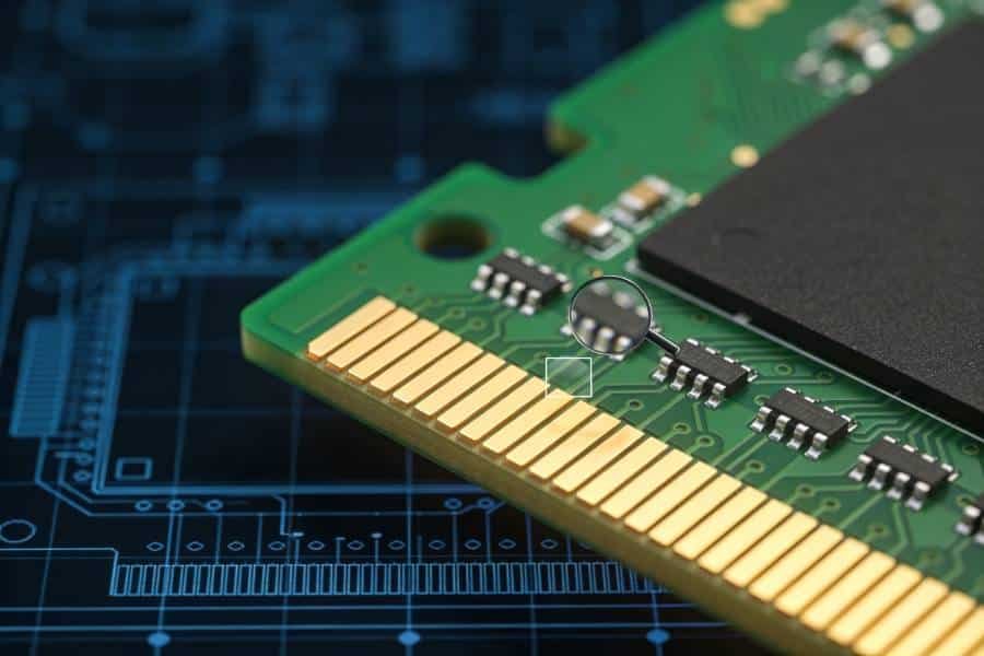
ENIG (electroless nickel immersion gold) is a chemical plating process that deposits a layer of nickel and then a very thin layer of gold over exposed copper pads on the PCB. In the first step, an autocatalytic reaction builds up a uniform nickel‑phosphorus layer that serves as a barrier between the copper and the final gold surface. The board is then immersed in a gold solution that displaces nickel atoms on the surface, forming a thin, conformal gold layer typically around 1–3 micro‑inches thick.
Because the ENIG process is immersion‑based and self‑limiting, it produces an extremely flat, solderable surface that is ideal for BGA pads, fine‑pitch components and general SMT assembly. The gold is relatively soft and thin, which is perfect for protecting the underlying nickel during storage and reflow but not designed to withstand heavy mechanical wear from repeated insertion and removal. For this reason, many PCB stack‑ups use ENIG as the main finish across the board while reserving other treatments for high‑wear areas.
Hard gold electroplating in brief
Hard gold, sometimes called electroplated gold, is applied using an electrolytic process that selectively plates gold onto specific areas of the PCB, most commonly the edge‑connector fingers. The typical build‑up is copper pad, followed by a relatively thick nickel underlayer, and then a gold alloy that includes small amounts of other metals—such as cobalt or nickel—to increase hardness and wear resistance. Unlike ENIG, hard gold thickness can be controlled over a wide range, often from 10 to 50 micro‑inches or more, depending on the required mating cycle life.
Because the plating is directional and current‑driven, hard gold is usually applied only where needed, using dedicated bus bars and masking to focus the deposition on the gold finger area. The resulting surface is harder and more abrasion‑resistant than ENIG, making it much better suited to connectors, switch contacts and other locations where metal‑to‑metal wiping occurs repeatedly. The trade‑off is that hard gold is more expensive per unit area and does not offer the same ultra‑flat solderability as ENIG, so it is rarely used as a universal finish across an entire board.
What this means specifically for PCB gold fingers
For PCB gold fingers, the differences between ENIG and hard gold become very significant. ENIG provides an excellent protective and solderable surface for pads that are assembled once and rarely touched again, but its thin, soft gold layer can wear through quickly if the edge connector is plugged and unplugged repeatedly. Hard gold, with its thicker and harder plating, is specifically engineered to survive hundreds or even thousands of mating cycles without exposing the nickel or copper beneath.
As a result, ENIG‑coated gold fingers are generally acceptable only for low‑cycle applications, prototypes or situations where the connector is more of an occasional test point than a primary interface. For production edge connectors in computers, networking gear, industrial control and other high‑reliability systems, hard gold is usually the recommended choice, often applied selectively on the fingers while the rest of the PCB uses ENIG or another cost‑effective finish. Understanding these fundamental process and performance differences is the foundation for making a sound decision between ENIG and hard gold on your next gold finger PCB.
Performance Comparison: Hard Gold vs ENIG on Gold Fingers
Durability and wear resistance
For PCB gold fingers, durability under repeated insertion and removal is usually the first comparison point between ENIG and hard gold. ENIG’s thin, soft gold layer is excellent for protecting the nickel during storage and soldering, but it is not designed to handle heavy mechanical wiping from connector springs. After a relatively small number of mating cycles, the immersion gold can wear through, exposing the nickel layer, which has higher contact resistance and is more susceptible to fretting and corrosion in the presence of vibration or contamination.
Hard gold, by contrast, is formulated and deposited specifically to maximize wear resistance. The thicker, harder alloy layer can survive hundreds or even thousands of mating cycles, depending on thickness and connector design, before any significant wear reaches the nickel underlayer. This is why hard gold is the default recommendation for high‑cycle edge connectors in computers, networking equipment and industrial control systems, while ENIG is generally reserved for low‑cycle or prototype use on fingers.
Solderability and assembly behaviour
ENIG was originally developed as a solderable finish, so its behaviour during assembly is one of its strongest advantages. The combination of a smooth nickel layer and very thin gold produces a flat, wettable surface that works well with modern lead‑free solders, especially on BGA lands, fine‑pitch pads and components that require good co‑planarity. Flux can easily remove the thin gold layer during reflow, allowing solder to bond to the nickel beneath and form reliable joints.
Hard gold is not usually chosen for its solderability. The thicker, harder gold alloy is more difficult for solder to dissolve, which can lead to brittle intermetallics and poor joint quality if you attempt to solder directly to heavily plated hard‑gold pads. For this reason, designers typically avoid using hard gold on pads intended for permanent solder connections and restrict it to areas used primarily for mechanical contact, such as gold fingers, key contacts or test points. In mixed‑finish designs, it is common to specify hard gold only on the connector fingers and ENIG (or another solderable finish) on the rest of the board to get the best of both worlds.
Corrosion resistance and reliability issues
Both ENIG and hard gold offer excellent resistance to oxidation compared with bare copper or many other finishes. However, each has its own reliability considerations that become more important in demanding environments. ENIG can suffer from issues such as “black pad” if the nickel‑phosphorus layer is not controlled properly, leading to brittle interfaces and potential contact or solder‑joint failures. While reputable fabricators have process controls to minimize this risk, it remains a known failure mode that must be considered for high‑reliability designs.
Hard gold does not have the same black‑pad mechanism, but if the plating is too thin or applied over poorly controlled nickel, heavy wear can still expose reactive layers that corrode or frett over time. In highly corrosive or high‑humidity environments, the thicker and harder gold layer generally provides a better safety margin for edge connectors, especially when combined with appropriate sealing, cleaning and material choices on the mating connector. Overall, both finishes are capable of long service life when correctly specified and processed, but hard gold tends to be the safer choice for gold fingers that will see both mechanical wear and harsh conditions.
Electrical performance and high‑frequency behaviour
From an electrical standpoint, both ENIG and hard gold provide low initial contact resistance and good conductivity. The underlying nickel layer, which is present in both processes, has higher resistivity than copper and can introduce additional loss at very high frequencies, but in most edge‑connector applications the physical length of the gold finger contact is short enough that this effect is acceptable. The more pressing concern is maintaining consistent, low‑resistance contact over the lifetime of the product, which again depends heavily on wear behaviour and environmental stability.
For very high‑speed interfaces or RF applications, designers sometimes pay closer attention to the exact geometry and materials of the connector, including the thickness and composition of the nickel and gold layers. In these cases, maintaining a smooth, uncontaminated contact surface and avoiding partial wear‑through of the gold layer can be more important than the subtle differences between ENIG and hard gold conductivity. In practice, many high‑speed edge connectors still rely on hard gold for its proven wear characteristics, while careful connector design and controlled impedance routing address the signal‑integrity aspects of the interface.
Cost and Process Considerations
Relative cost: ENIG vs hard gold
From a cost perspective, ENIG is usually treated as a mainstream, moderately priced finish, while hard gold is considered a premium option reserved for specific high‑wear areas. ENIG uses a chemical immersion process that deposits only a very thin layer of gold over nickel, so the amount of precious metal consumed per panel is relatively small and well controlled. Hard gold, on the other hand, builds up a much thicker layer of gold alloy through electroplating, which requires more gold, longer plating times and tighter process control.
As a result, switching from ENIG to hard gold on the same area generally increases cost, and moving from thin to heavy hard‑gold thickness levels increases it further. The exact premium depends on the fabricator, gold price and panel utilization, but it is common for hard‑gold options on gold fingers to add a noticeable percentage to the PCB price compared with an ENIG‑only design. This is why many designers try to limit hard gold to the minimum area necessary for reliable connectors.
Selective plating: hard gold only where you need it
The good news is that you rarely need to choose between “all ENIG” and “all hard gold” for an entire board. Most PCB manufacturers can plate hard gold selectively on the gold finger region while finishing the rest of the board with ENIG or another solderable finish. In this common hybrid approach, the edge connector receives a thick, wear‑resistant hard‑gold coating, while the majority of pads and component lands use ENIG for its solderability and lower cost.
Selective plating does introduce additional process steps, such as masking and dedicated plating rails, but these are well‑understood operations in board houses that regularly produce gold finger PCBs. By confining the hard‑gold area to the fingers, you minimize gold consumption and keep the cost impact proportional to the actual connector length rather than the entire board surface. This strategy is one of the most effective ways to combine ENIG and hard gold without over‑spending.
Panelization and fabrication constraints
When planning a design that uses hard‑gold fingers, it is important to consider how the boards will be panelized and processed. Some fabricators require that all gold finger edges in a panel face the same direction or be located on the panel perimeter to simplify plating, beveling and handling. There may also be minimum length or spacing requirements for the finger region to ensure uniform plating thickness and reliable chamfering.
If these constraints are not taken into account during layout and panel design, you may face additional engineering time, panel redesign charges or limitations on how tightly boards can be nested. Early communication with your PCB vendor about where the gold fingers are located, how many boards per panel you expect and what bevel angles you require can prevent surprises at the quotation stage. In some cases, small adjustments to board outline, connector orientation or panel break‑off features can significantly reduce complexity and cost for hard‑gold processing.
Application‑Based Recommendations
When ENIG on gold fingers is acceptable
There are many situations where ENIG on the gold finger area is perfectly acceptable and can save cost. These include prototypes, evaluation boards, low‑volume lab fixtures and products where the edge connector is mated only a few times during assembly and service. In clean, controlled environments with low mating cycles, the thin immersion gold layer provides adequate protection and conductivity, especially if the connector is not subjected to frequent vibration or hot‑swapping.
ENIG can also be a reasonable choice when the gold fingers are primarily used as occasional test contacts or programming interfaces rather than as a primary high‑cycle field connector. In such cases, using a single ENIG finish across the entire PCB simplifies fabrication, keeps the price down and still meets the functional requirements, provided you are comfortable with the limited wear life of the immersion gold layer.
When you should insist on hard gold
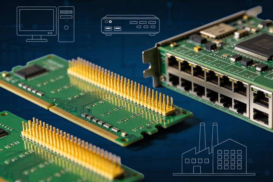
For production edge connectors that will see regular use, hard gold is usually the safer and more appropriate choice. Typical examples include PCIe and other card‑edge interfaces in computers and servers, plug‑in line cards in networking and telecom equipment, industrial control modules, and test fixtures or programming adapters that are connected and disconnected frequently. In these applications, the connector may experience hundreds or even thousands of mating cycles over the life of the product, often in environments that are less than perfectly clean.
Using hard gold on the fingers provides a thicker, harder contact surface that maintains low, stable resistance under repeated mechanical wiping and environmental stress. The incremental cost of selective hard‑gold plating on the edge connector is usually small compared with the cost of field failures, service calls or downtime caused by worn‑out contacts. As a result, most high‑reliability design guidelines explicitly recommend hard gold for gold fingers whenever frequent mating or harsh conditions are expected.
Mixed strategies in complex systems
Modern systems often combine multiple types of boards and connectors with different usage patterns and reliability targets. For example, a telecom chassis might contain high‑cycle line cards, low‑cycle configuration modules and internal adapter boards that are rarely removed. Applying the same finish to every gold finger in such a system is rarely optimal from a cost‑performance standpoint.
A more nuanced strategy is to use ENIG on gold fingers where mating cycles are low and cost pressure is high, while specifying hard gold on connectors that are critical or frequently handled. Your PCB supplier can help you implement this approach by producing different board variants with finishes tailored to their roles, or by selectively plating only specific edge connectors with hard gold while keeping others on ENIG or thin gold. This way, you pay for hard‑gold durability only where it truly matters, without over‑engineering every connector in the system.
Practical Selection Checklist (ENIG vs Hard Gold)
Use the following checklist when deciding whether your PCB gold fingers should use ENIG, hard gold, or a mix of both.
1. Mating cycles
- The connector will be mated only a few times (prototype, lab, one‑time installation) → ENIG or thin hard gold may be acceptable.
- The connector will be mated occasionally over many years (maintenance, occasional module swaps) → Prefer hard gold with medium thickness.
- The connector will be mated frequently or hot‑swapped (test fixtures, line cards, field‑replaceable modules) → Use hard gold with appropriate high‑cycle thickness.
2. Environment and criticality
- Clean, controlled environment; failures have low impact → ENIG on fingers can be considered to save cost.
- Industrial or telecom environment with dust, vibration or temperature variation → Prefer hard gold for more robust wear and corrosion margins.
- Safety‑critical, medical, military or high‑availability systems → Treat edge connectors as high‑reliability features and specify hard gold.
3. Electrical and functional role of the fingers
- Fingers mainly used as occasional test or programming contacts → ENIG or thin hard gold may be sufficient.
- Fingers are the primary interface for power, high‑speed data or system‑critical control signals → Use hard gold to maintain stable contact resistance over time.
4. Soldering requirements
- Do you need to solder directly to the gold finger area?
- Yes → Avoid heavy hard gold; prefer ENIG or a special solderable finish, and reconsider whether this area should function as a connector.
- No, fingers are only for mechanical contact → Hard gold is preferred for high‑wear connectors.
5. Cost sensitivity
- Project is highly cost‑sensitive and connectors are low‑cycle → Use ENIG on fingers or thin hard gold, and avoid heavy plating.
- Connector failures would be expensive to service or cause downtime → Accept the added cost of selective hard gold as insurance.
6. Fabrication capabilities and panelization
- Have you confirmed that your PCB supplier supports selective hard‑gold plating on gold fingers with ENIG elsewhere on the board?
- Yes → Use a hybrid strategy: hard gold on fingers, ENIG on pads.
- <p[&_strong:has(+br)]:pb-2″> No → Discuss options early; you may need to adjust panelization, bevel angles or finish selection.
7. Final decision summary
After working through the checklist, you should be able to answer:
- Finish for gold fingers: ENIG / thin hard gold / medium hard gold / heavy hard gold
- Finish for the rest of the board: ENIG / HASL / OSP / other
- Rationale: brief note combining mating cycles, environment, cost and fabricator feedback.
Documenting this decision in your design notes and fabrication drawing helps align expectations between design, purchasing and manufacturing, and makes future design reviews much easier.
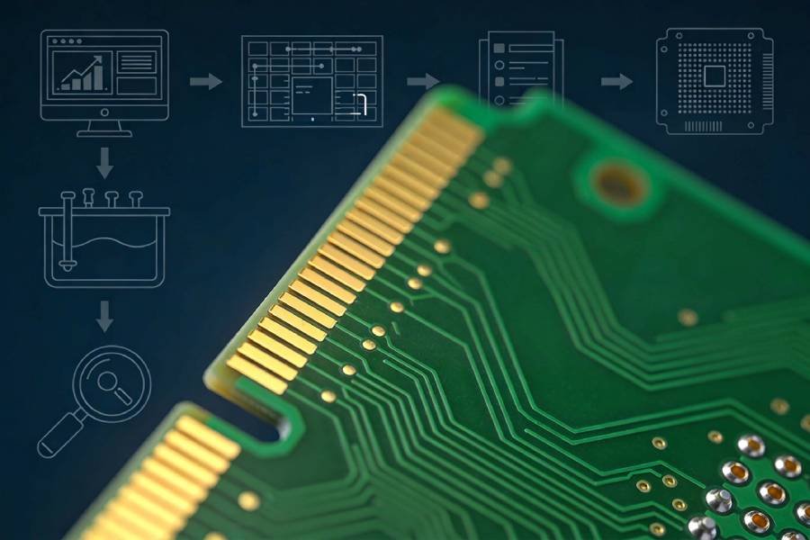
How JHYPCB Can Help You Choose the Right Finish
For many engineers, the real challenge is not understanding the theory, but turning requirements like “about 500 mating cycles in an industrial environment” into a concrete finish specification that a PCB factory can execute reliably. This is exactly where a specialized gold finger manufacturer like JHYPCB adds value, by combining process capability (hard gold 3–50 µin, 30°–45° bevels, selective plating) with practical design feedback before production.
JHYPCB offers a dedicated “Gold Finger PCB fabrication & manufacturing service” with hard gold plating from 3–50 µin, 30°–45° bevels, and fast prototype or small‑batch production.
When you submit your Gerber files and requirements, JHYPCB’s CAM and engineering team can review not only the overall stack‑up and clearances, but also whether your gold finger area, bevel angle and surface finish choice match the intended application. If there is a mismatch—for example, ENIG fingers specified for a very high‑cycle connector, or hard gold specified on pads that must be soldered—they can recommend adjustments early so you do not discover issues at assembly or in the field.
In practice, that often means helping you move from a generic note like “gold fingers” to a more precise and manufacturable call‑out such as “hard gold 30–50 µin on gold fingers, 30° bevel, ENIG on all other pads.” By aligning gold thickness, bevel angle, and selective plating strategy with your real mating cycles and cost targets, JHYPCB helps you balance reliability and budget instead of over‑ or under‑specifying the finish.
If you are still early in the design phase, JHYPCB can also provide DFM input on panelization, connector orientation and keep‑out around the edge to ensure the fingers can be plated and beveled correctly. This kind of early collaboration reduces the risk of last‑minute engineering holds, and shortens the path from first prototype to stable small‑batch and volume production.
Conclusion
Choosing between ENIG and hard gold for your gold fingers is not just a question of “which finish is better”, but of how many mating cycles you expect, what environment the connector will see, and how critical those contacts are to system reliability. By translating these application requirements into concrete parameters such as gold thickness, bevel angle and selective plating strategy, you can avoid both over‑specification that wastes budget and under‑specification that risks intermittent failures in the field.
In practice, this often leads to a hybrid approach: hard gold on the edge connectors that see frequent insertion and removal, ENIG or other solderable finishes on the rest of the board, and careful attention to panelization and DFM so that the fingers can be plated and beveled consistently. Working with an experienced manufacturer like our “Gold Finger PCB manufacturing service” makes it much easier to validate these decisions before you commit to tooling and volume builds.
If you are currently evaluating ENIG vs hard gold for a new design, you can send your files and basic usage requirements (mating cycles, environment, reliability expectations) to JHYPCB and request a focused DFM review for the gold finger area. Our engineering team can help you turn high‑level statements like “industrial control, hundreds of mating cycles” into a clear, manufacturable finish specification and provide an instant quote for prototypes and small‑batch builds.
You can learn more about our Gold Finger PCB capabilities—hard gold 3–50 µin, 30°–45° bevels, selective plating and fast lead times—and upload your project files directly on our Gold Finger PCB service page. If you are unsure how to specify the finish on your drawing, just describe the application and connector usage in your inquiry, and we will recommend an appropriate ENIG/hard‑gold combination before production.