Table of Contents
Why a Gold Finger DFM Checklist Matters
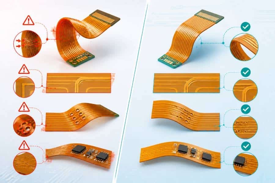
Gold finger PCBs are unforgiving when it comes to DFM: small mistakes at the edge connector can slip through design reviews and only appear as intermittent field failures months later. Issues like fingers too close to the edge, unclear bevel notes, missing mask openings, or ambiguous gold thickness can all lead to scrap, re‑spins, or unreliable connections that are hard to debug.
A focused DFM checklist gives you a structured way to catch these problems before you send Gerber files to your fabricator. The ten points below are tailored specifically to gold finger PCBs and can be used as a last “pre‑flight” step alongside your manufacturer’s general DFM rules. If you are unsure about any item on the list, you can flag it explicitly when you submit your files through our “Gold Finger PCB Fabrication & Manufacturing Service” so the engineering team knows what to double‑check.
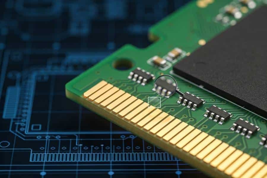
1. Confirm gold finger location, length, and orientation
Before exporting Gerbers, verify that the gold fingers are placed on the correct board edge that matches your mating connector and mechanical drawing. The connector outline in your PCB CAD should align with the board edge and finger row, and there should be no ambiguity about which side of the board plugs into the socket.
Check that finger length is sufficient for full engagement with the connector but not so long that it risks bending or interfering with mechanical guides. All fingers that belong to the same connector should be aligned and of consistent length unless you intentionally use staggered lengths for power sequencing or make‑before‑break behavior.
At the panel level, confirm that all gold finger edges for that design are oriented in the same direction on the panel, so plating and beveling can be done consistently. If you are unsure about preferred orientation, you can add a brief note in your fab drawing and mention it in your Gold Finger PCB quote/DFM request so the fabricator can confirm or suggest adjustments.
2. Check bevel angle, clearance to pads, and board thickness
Next, make sure your fabrication notes clearly specify the bevel angle and whether it applies to one or both sides of the connector edge. Common values are 30° or 45°, often dictated by the mating connector datasheet, and they affect how much material is removed at the edge as well as how easily the board inserts into the slot.
Measure the distance from the end of each finger pad to the finished board edge in your CAD or Gerber viewer. Most manufacturers recommend roughly 0.6–1.0 mm clearance (depending on board thickness and angle) so the bevel does not cut into the plated contact area. If your current design does not meet this, adjust either pad‑to‑edge spacing or the requested bevel depth before release.
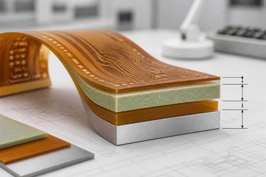
Finally, verify that the board thickness at the connector matches the specification for the mating socket (for example, 1.6 mm vs 2.0 mm) and that your layer stack supports this value. Many edge connectors are optimized for a narrow thickness range; sending a different thickness to your PCB house without updating the mechanical design can cause poor fit and unreliable contact.
3. Verify solder mask openings and no‑mask zone on fingers
Gold fingers must be completely free of solder mask so that nickel and hard gold can plate directly onto clean copper. Before sending Gerbers, open your solder mask layers in a viewer and confirm that each finger has a full, continuous mask opening that extends cleanly to the board edge with no thin mask “slivers” left between fingers.
Check that there is no mask accidentally covering part of a finger due to incorrect pad stack, layer mapping, or mask expansion rules. Any residual mask on the contact area can block plating and lead to intermittent contact or early wear in service. Also verify that silkscreen, polarity marks, logos, and text are kept well away from the gold finger region on both sides to avoid contamination and visual clutter during inspection.
If you use different mask clearances globally and locally, make sure the gold finger region is exempt from any automatic “solder mask defined” behavior. When in doubt, you can add a short note like “No solder mask or legend on gold finger contacts” in your fab drawing and ask your manufacturer, via a Gold Finger PCB DFM request, to confirm that their CAM interpretation matches your intent.
4. Confirm surface finish split: hard gold on fingers vs finish on pads
Gold fingers typically require a different surface finish from the rest of the board. In most designs, the edge contacts use nickel plus hard gold for wear resistance, while component pads use ENIG, HASL, OSP, or another solderable finish optimized for assembly rather than mating cycles.
Before releasing your files, confirm that your fabrication notes clearly distinguish these areas instead of using a vague “ENIG with gold fingers” statement. A better call‑out might be “Hard gold over nickel on edge connector fingers; ENIG on all other exposed pads,” or a similar explicit description that your PCB house can implement in their process.
Make sure your Gerber and drawing set does not inadvertently define the entire outer layer as gold‑plated by using a generic “gold” note without limiting it to the finger region. This can cause unexpected cost increases or CAM questions. If you are not sure how to phrase the split finish, you can reuse wording from your manufacturer’s Gold Finger PCB Fabrication & Manufacturing Service design guidelines or ask them to suggest a standard note that fits your application.
5. Check copper pull‑back and inner‑layer clearances near the edge
Gold finger edges should not expose internal copper when the board is routed and beveled. Before sending Gerbers, review your stack‑up and inner‑layer artwork to confirm that planes and traces are pulled back from the connector edge by a safe distance, taking bevel depth into account.
Many manufacturers recommend additional pull‑back under the finger region compared with the rest of the outline, to prevent internal copper “telegraphing” through the edge after machining. Use your CAD tool’s section view or a dedicated DRC rule to verify that no inner‑layer copper comes closer to the edge than your fabricator’s guideline for gold finger boards.
6. Enforce keep‑outs: no vias, test pads, or labels in the finger zone
The gold finger zone should be treated as a protected contact area, not a place for vias, test pads, or mechanical features. In your design rules and Gerbers, confirm that there are no plated through‑holes, microvias, or via‑in‑pad features within at least about 1–2 mm of the finger base and beveled edge.
Likewise, keep test points, debug headers, and large copper features away from the connector side, so they do not interfere with plating, beveling, or insertion into the mating connector. Make sure these keep‑outs are also respected in your panel drawing—no tooling holes, fiducials, or break‑off tabs should encroach into the defined “no‑go” band around the gold finger edge.
Review panelization: orientation, rails, and tabs around the connector edge
Panelization can make or break gold finger yield, so include it in your DFM check instead of treating it as a separate topic. Verify that all gold finger edges for a given design are oriented in the same direction on the panel and, where possible, placed along a common panel side to simplify plating and beveling.
Check that break‑off tabs, mouse bites, and V‑score lines are kept away from the connector edge, with sufficient distance so depanelization stress does not chip the bevel or crack the laminate near the fingers. Ensure there are adequate rails and tooling holes on non‑connector sides of the panel so the array can be handled and processed without clamping directly on the gold finger edge.
8. Define gold thickness and mating‑cycle requirements clearly in fab notes
Gold thickness on the fingers is tightly linked to expected mating cycles and cost, so it should never be left as an implied or generic value. In your fabrication notes, specify the target hard‑gold thickness range (for example, 30–50 µin) and, ideally, the approximate mating‑cycle requirement that drove that choice.
Avoid vague phrases like “gold fingers as standard” that leave room for different interpretations between suppliers or even between builds. If you are not certain what thickness you need, state your estimated cycles and environment (lab prototype vs high‑cycle test fixture vs industrial line card) and ask your manufacturer—via a Gold Finger PCB Fabrication & Manufacturing Service request—to recommend a practical range that balances reliability and cost.
9. Add inspection and measurement notes for plating and bevel (when relevant)
For gold finger PCBs that are safety‑critical, high‑cycle, or expensive to service, it is worth defining how plating and bevel quality will be verified. In your fab drawing, you can request XRF sampling for nickel and gold thickness on the finger area, tape tests for adhesion, and visual inspection of the bevel angle and edge quality against IPC‑style criteria.
These notes do not need to be long, but they should indicate which features are critical (for example, “gold thickness on fingers” or “30° bevel on connector edge”) so the manufacturer knows where to focus their QA checks. If you add such requirements, make sure they are aligned with what your Gold Finger PCB supplier can realistically support within your cost and lead‑time targets, and adjust them after discussing trade‑offs if necessary.
10. Validate that Gerbers and drawings reflect all of the above
Finally, do a holistic pass to ensure that your Gerber files, fabrication drawing, and any separate panel drawing are consistent with each other and reflect every decision from this checklist. Use an independent Gerber viewer to verify pad‑to‑edge distances, mask openings, copper pull‑backs, keep‑outs, and panel features exactly as they will appear at the fabricator.
Check that your notes on bevel angle, gold thickness, surface finish split, and inspection expectations are present, unambiguous, and not contradicted by legacy or boilerplate text. If you are sending the design to JHYPCB or another specialist, you can include this DFM checklist (or a short summary of any uncertainties) with your “Gold Finger PCB Fabrication & Manufacturing Service” inquiry so the engineering team can confirm you did not miss a critical edge‑connector detail before production starts.
Conclusion
A lot of gold finger problems that show up during fabrication, assembly, or in the field can be traced back to details that were never checked before the Gerber files were sent out. By running through a focused DFM checklist—covering geometry, beveling, mask openings, finish splits, copper clearances, keep‑outs, panelization, gold thickness, inspection, and documentation—you greatly reduce the chances of expensive re‑spins and intermittent connector issues later.
The goal is not to make your design “perfect” on the first try, but to ensure that everything your manufacturer needs to build a reliable gold finger PCB is clearly defined and visible in the data you provide. If you still have doubts on any of the ten points, you can attach this checklist to your next order via our “Gold Finger PCB Fabrication & Manufacturing Service” page and ask for a DFM review focused specifically on the edge connector area, so potential issues are caught while they are still easy to fix.