Table of Contents
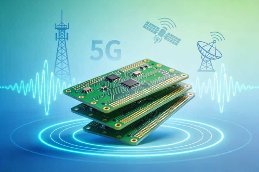
In modern electronics, more and more systems are pushing into the RF and microwave range, from 5G base stations and Wi‑Fi routers to automotive radar and satellite communication terminals. At these frequencies, a printed circuit board is no longer just a simple carrier for copper traces and components – it becomes a critical part of the signal path that directly affects loss, impedance, noise and overall system performance.
This is where high frequency PCBs come in. A high frequency PCB is specifically designed to carry RF and microwave signals with minimal loss and distortion, using low‑loss materials, controlled impedance routing and carefully engineered stackups. Understanding what a high frequency PCB is, how it differs from a standard board, and where it is used is the first step before diving into detailed design rules or talking with a high frequency PCB manufacturer about your next project.
What Is a High Frequency PCB?
Definition and Frequency Range
There is no single universal cutoff frequency that defines a “high frequency PCB”, and different sources use slightly different thresholds. Some references start calling a board “high frequency” once signal frequencies exceed a few hundred megahertz, while others reserve the term for designs operating above 1 GHz, in the RF and microwave range. In practical engineering, high frequency PCBs usually refer to boards that must reliably carry RF or microwave signals from hundreds of megahertz up to several gigahertz or even tens of gigahertz, where transmission line effects and material properties dominate behavior.
What really distinguishes a high frequency PCB from a standard digital or power board is not the copper itself, but the combination of materials, stackup and geometry required to control signal behavior at these frequencies. High frequency PCBs use low‑loss dielectric materials with well‑controlled dielectric constant, carefully defined layer structures and impedance‑controlled traces, so that signal attenuation, reflections and phase distortions stay within acceptable limits. Manufacturing tolerances such as dielectric thickness, trace width, spacing and copper roughness also become much more critical than in typical low‑speed designs, so the board must be designed and fabricated with RF performance in mind from the start.
In many projects, high frequency PCBs are also part of mixed‑signal systems that combine RF front‑ends with high‑speed digital processing on the same board or in the same module. In these cases, designers often rely on hybrid constructions, where RF sections use specialized high frequency materials and digital/control sections use high performance FR4, to balance signal integrity, manufacturability and overall cost. Working closely with an experienced high frequency PCB manufacturer helps ensure that the chosen materials, stackup and design rules can be realized consistently in volume production, not just in theory.
Key Differences Between High Frequency and Standard PCBs
At first glance, a high frequency PCB may look very similar to a standard PCB, with copper traces, vias and components mounted on a laminate substrate. However, once signal frequencies move into the RF and microwave range, several aspects that are almost negligible in low‑speed designs become critical to performance. The main differences appear in the choice of base materials, the way layer stackups are engineered, the level of control over trace geometry and impedance, and the tighter manufacturing tolerances required.
In a standard PCB, FR4 is often sufficient as a core material, and its dielectric constant and loss may only have a modest effect on signal quality at lower frequencies. In a high frequency PCB, designers typically use low‑loss laminates such as PTFE, ceramic‑filled or hydrocarbon materials, where dielectric constant (Dk) and dissipation factor (Df) are tightly specified and stable over frequency and temperature. Stackups are carefully planned with dedicated reference planes and controlled dielectric thicknesses so that RF traces behave as well‑defined transmission lines rather than simple wires.
Manufacturing and layout rules are also more demanding in high frequency designs. Trace width and spacing must be controlled within tighter tolerances to maintain target impedance, and copper surface roughness, drilling accuracy and plating quality can all have a measurable impact on insertion loss and signal integrity. Design practices such as minimizing discontinuities, providing clean return paths, avoiding poorly thought‑out split planes and managing crosstalk are essential, and they need to be aligned with what the chosen high frequency PCB manufacturer can reliably produce in volume.
Key Material Properties of High Frequency PCBs
High frequency PCBs rely heavily on the electrical properties of their dielectric materials, because these properties directly determine how RF and microwave signals propagate along the traces. While mechanical strength, thermal reliability and manufacturability still matter, parameters such as dielectric constant (Dk), dissipation factor (Df), stability over frequency and temperature, and even copper roughness become critical design inputs rather than afterthoughts.
Dielectric Constant (Dk)
The dielectric constant describes how much a material slows down an electromagnetic wave compared with air and strongly influences both characteristic impedance and signal propagation velocity on a PCB trace. In high frequency PCBs, designers typically choose materials with well‑controlled, relatively stable Dk values so that impedance can be accurately predicted and matched across the operating frequency range. Popular high frequency materials such as Rogers RO4350B, RO4003C or PTFE‑based laminates specify Dk within tight tolerances and provide data over a range of frequencies to support precise RF design.
Dissipation Factor (Df)
Dissipation factor, sometimes called loss tangent, describes how much signal energy is lost as heat when an electromagnetic wave travels through the dielectric. At RF and microwave frequencies, even modest dielectric losses can accumulate over long trace lengths, leading to significant insertion loss and reduced link budget. High frequency PCB materials are therefore selected for very low Df values at the target frequency, so that filters, transmission lines and antennas maintain their designed performance with minimal additional loss from the substrate itself.
Stability over Frequency and Temperature
For many RF and microwave applications, it is not enough for Dk and Df to be low; they also need to remain stable as frequency and temperature change. Variations in dielectric properties can shift impedance, detune filters and antennas, and cause drift in phase‑sensitive circuits, which is especially problematic in wideband communication systems or radar. High frequency PCB materials are therefore characterized over a range of frequencies and operating temperatures, and manufacturers provide detailed datasheets so engineers can evaluate whether a material will stay within acceptable tolerances in the field.
Copper Roughness and Other Factors
At high frequencies, conductor losses become more sensitive to copper surface roughness because current tends to flow near the surface of the conductor (skin effect). Rougher copper increases effective path length and resistance, which adds insertion loss on top of dielectric loss, so many high frequency PCB designs benefit from using smoother copper foils or carefully specified copper types. Other factors such as coefficient of thermal expansion (CTE), thermal conductivity and moisture absorption can also influence reliability and RF performance, particularly in applications with large temperature swings or humid environments.
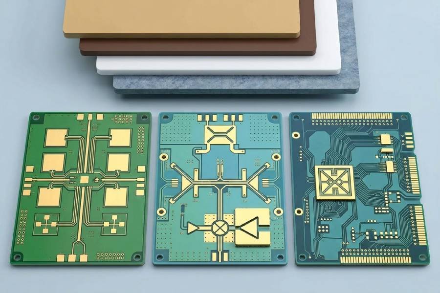
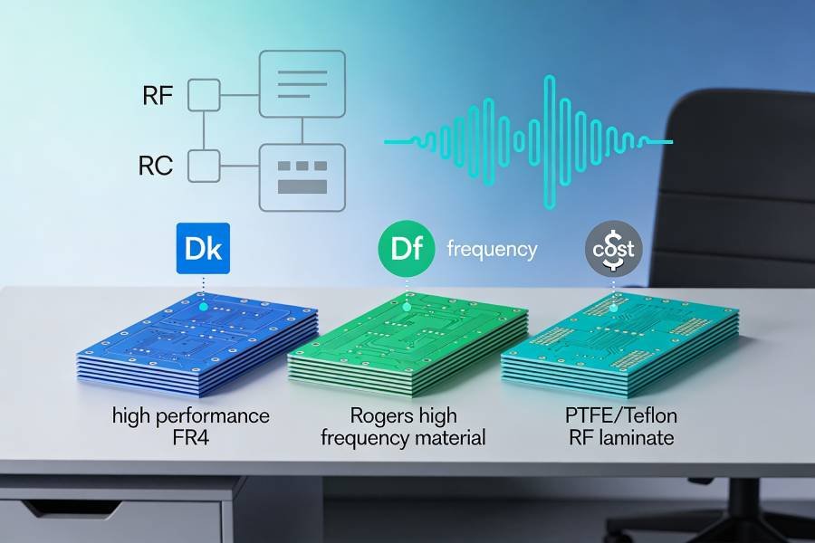
Common High Frequency PCB Materials
High frequency PCBs are built on dielectric materials that are engineered for low loss, stable dielectric properties and predictable behavior at RF and microwave frequencies. In practice, many designs use a combination of PTFE‑based laminates, hydrocarbon/ceramic materials and high performance FR4, sometimes in hybrid stackups where different layers serve different functions.
PTFE‑Based High Frequency Materials
PTFE (polytetrafluoroethylene)‑based laminates are widely used when ultra‑low loss and very stable dielectric properties are required at high frequencies. These materials offer very low dissipation factor, tightly controlled dielectric constant and excellent high frequency performance, which makes them suitable for microwave filters, antennas, couplers and long RF transmission lines. Many well‑known high frequency materials, including certain Rogers and Duroid laminates, fall into this PTFE‑based category and are common in advanced radar, satellite communication and aerospace systems where every decibel of loss matters.
Rogers Hydrocarbon/Ceramic Laminates
Rogers RO4000 series hydrocarbon/ceramic laminates, such as RO4003C and RO4350B, are popular because they provide high frequency performance close to PTFE materials while being easier to process with standard FR4 manufacturing methods. These materials offer stable dielectric constant and low loss over a broad frequency range, along with good thermal and mechanical properties, making them suitable for RF front‑end modules, 5G antennas, base station boards and many microwave applications. Because their fabrication requirements align closely with mainstream PCB processes, they are often chosen as a cost‑effective middle ground between standard FR4 and more demanding PTFE‑based substrates.
High Performance FR4 and Modified FR4
Standard FR4 is generally not ideal for very high frequency applications due to higher dielectric loss and less stable dielectric constant, but modified high performance FR4 materials can still be useful in certain high frequency or high‑speed designs. These improved FR4 laminates feature lower Dk and Df, better thermal properties and tighter tolerances, making them suitable for shorter RF paths, high‑speed digital layers, power distribution and control circuitry in mixed‑signal systems. In many real‑world designs, high performance FR4 is combined with RF materials so that sensitive RF layers use low‑loss substrates while less critical layers use more economical laminates.
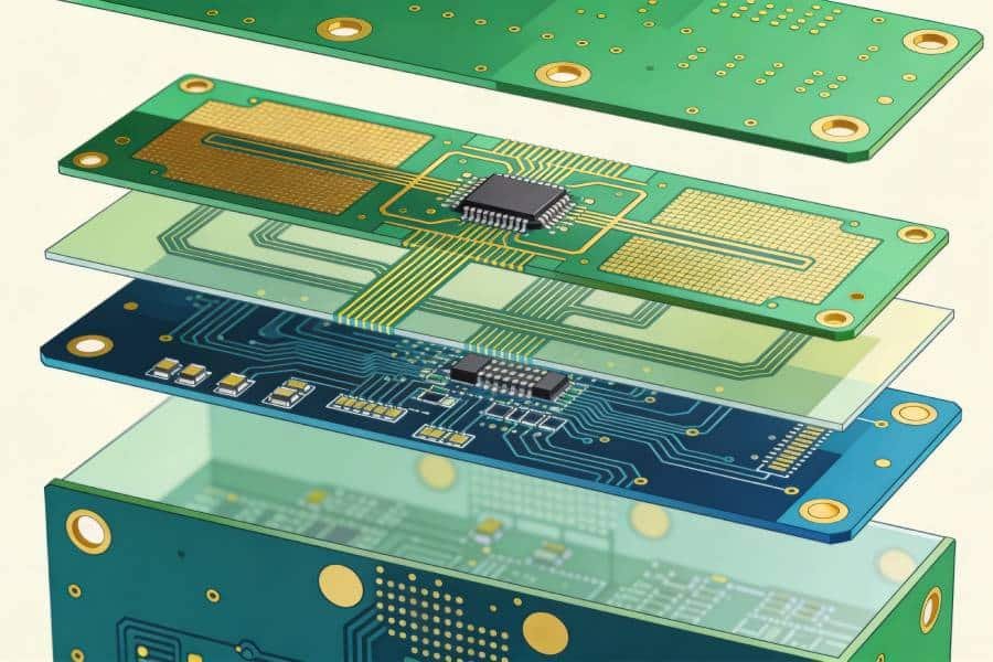
Hybrid High Frequency PCB Constructions
Hybrid high frequency PCBs use different materials in the same stackup, typically routing RF signals on Rogers or PTFE‑based layers and using high performance FR4 for digital, control and power planes. This approach allows designers to place low‑loss, controlled impedance RF structures exactly where they are needed, while keeping overall board cost and manufacturability under control. Successful hybrid designs require careful stackup planning, attention to thermal expansion differences and close collaboration with a high frequency PCB manufacturer to ensure that lamination, drilling and plating processes can accommodate the mixed materials reliably.
Typical Frequency Ranges and Applications
Because “high frequency” is a relative term, it is helpful to look at typical frequency bands and the kinds of applications that usually fall into each range. In practice, many boards that engineers call high frequency PCBs operate from a few hundred megahertz up to several gigahertz or higher, often overlapping with high‑speed digital designs that share similar signal integrity challenges.
Typical Frequency Ranges
In the sub‑GHz range, roughly from a few hundred megahertz up to around 1 GHz, high frequency PCBs are commonly used for legacy cellular systems, ISM band radios, certain radar sensors and lower‑frequency communication links. Between about 1 GHz and 6 GHz, many modern wireless systems operate, including Wi‑Fi, LTE and 5G Sub‑6 GHz, where controlled impedance, low loss and crosstalk management become increasingly important for both RF and high‑speed digital signals. Above these ranges, in the microwave and millimeter‑wave bands, high frequency PCBs support applications such as automotive radar around 24 GHz and 77 GHz, satellite communication links and specialized point‑to‑point radios, where material choice and manufacturing precision are even more critical to achieve acceptable loss and phase stability.
Common Application Areas
In wireless communication, high frequency PCBs are used in 5G base stations, small cells, remote radio heads, Wi‑Fi access points and customer premises equipment, carrying RF front‑end signals, power amplifiers and matching networks. Automotive and industrial radar systems rely on high frequency PCBs to implement antennas, transmit/receive modules and signal conditioning circuits that must remain stable over wide temperature ranges and harsh environments. Satellite and aerospace systems use high frequency PCBs in ground terminals, on‑board transponders and RF front‑ends, where low loss, reliability and material stability are essential over long mission lifetimes.
Beyond pure RF, many high‑speed digital and mixed‑signal systems also fall into the high frequency PCB domain because their serial links, clocks and interfaces operate at multi‑gigabit data rates with fast edge transitions. In these designs, the same concerns—controlled impedance, low loss, crosstalk control and solid reference planes—apply to differential pairs and digital interconnects, often on the same board that carries RF circuits. As a result, understanding typical frequency ranges and application environments is an important step toward choosing appropriate materials, stackups and a high frequency PCB manufacturer that can support the required performance.
Basic Design Considerations for High Frequency PCBs
High frequency PCB performance depends not only on choosing the right materials but also on applying sound layout and stackup practices that treat traces as controlled transmission lines, not just wires. Even a good RF substrate can deliver poor results if impedance, return paths and coupling are not carefully managed in the PCB design.
Controlled Impedance and Stackup Planning
In high frequency PCBs, most critical RF and high‑speed digital traces are designed as transmission lines with specific characteristic impedance, such as 50 Ω single‑ended or 100 Ω differential. Achieving these targets requires a well‑defined stackup with known dielectric thicknesses, dielectric constants and copper thickness, combined with carefully calculated trace widths and spacing. Early collaboration with a high frequency PCB manufacturer to confirm feasible stackups and impedance tolerances helps avoid redesigns and ensures that simulated performance is achievable in production boards.
Routing and Return Path Control
At RF and high‑speed frequencies, signals always return through the path of least impedance, not just the shortest physical distance, which means the quality of the reference plane under a trace is critical. Designers should keep high frequency traces as short and direct as practical, avoid unnecessary stubs and sharp 90‑degree corners, and ensure that each critical line has a continuous reference plane beneath it with no splits or gaps that would force current to detour. Proper via placement and stitching vias near layer transitions help maintain low‑inductance return paths and reduce the risk of radiation and signal integrity issues.
Crosstalk and Spacing
As edge rates increase and signals move into the high frequency range, coupling between adjacent traces can cause crosstalk that degrades both RF and digital performance. Maintaining sufficient spacing between sensitive lines, using differential pairs with tight intra‑pair coupling and larger spacing to other nets, and routing orthogonally between adjacent layers are common techniques to reduce unwanted coupling. Ground guard traces and properly referenced stripline structures inside the stackup can also help mitigate crosstalk when board space is limited.
EMI/EMC and Power Integrity Basics
High frequency PCBs must also consider electromagnetic interference and power integrity, since poor decoupling, noisy power planes or poorly controlled current loops can radiate or pick up unwanted energy. Good practices include using solid reference planes, placing decoupling capacitors close to IC power pins, minimizing loop areas for high di/dt currents and avoiding unnecessary plane splits in critical return paths. Coordinating these design choices with the capabilities and recommendations of a high frequency PCB manufacturer helps ensure that the final board meets both functional performance and regulatory requirements.
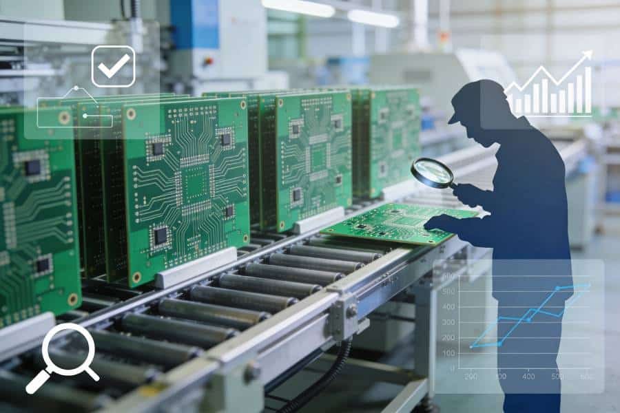
High Frequency PCB Manufacturing in Practice
From a manufacturing point of view, high frequency PCBs share many basic process steps with standard boards, but the tolerances, materials and process controls involved are significantly more demanding. Every stage—from incoming material inspection and lamination to drilling, etching and surface finishing—must be tuned to preserve the dielectric properties, dimensions and impedance targets defined in the design.
Manufacturing Challenges
One of the biggest challenges in high frequency PCB fabrication is dealing with specialized RF materials such as PTFE and ceramic‑filled laminates, which are more difficult to process than standard FR4. PTFE‑based substrates have low adhesion to copper, higher thermal expansion and a tendency to smear during drilling, so they require optimized lamination cycles, surface treatments and drilling parameters to achieve reliable vias and stable layer bonding. Even with more process‑friendly hydrocarbon/ceramic materials like RO4003C or RO4350B, tight control of dielectric thickness, resin flow and layer registration is needed to keep impedance and loss within specification.
Key Process Steps and Tolerances
In high frequency PCB manufacturing, etching, drilling and plating processes are typically run with tighter tolerances than for standard boards, because small deviations in trace width, spacing or via geometry can translate into measurable RF performance changes. Controlled‑impedance RF traces may require trace width tolerances on the order of ±0.5 mil or better, and the cross‑sectional shape of etched traces must be managed so that impedance calculations remain valid. Drilling PTFE‑based or hybrid stackups often demands special bit geometries, adjusted feed rates and careful desmear and surface preparation to prevent resin smear, ensure good copper adhesion and maintain via reliability at high frequencies.
Working with a High Frequency PCB Manufacturer
Because of these complexities, design teams gain a lot by involving their high frequency PCB manufacturer early in the project to review proposed materials, stackups and critical geometries. A capable high frequency PCB fabrication partner can flag potential manufacturability issues, suggest alternative materials or hybrid constructions and recommend realistic impedance tolerances that can be held in production, reducing the risk of costly redesigns and delays. Close collaboration between design and manufacturing ultimately helps ensure that the high frequency PCB not only performs well in simulation but also delivers consistent RF and high‑speed behavior across prototypes and volume builds.
How to Choose a High Frequency PCB Manufacturer
Selecting the right high frequency PCB manufacturer has a direct impact on whether your RF or high‑speed design meets its performance, cost and time‑to‑market targets. Beyond basic PCB capabilities, you need a partner that understands RF materials, controlled‑impedance stackups and the tighter process controls required for high frequency and microwave work.
Experience with RF and High Frequency Designs
An experienced high frequency PCB manufacturer should be able to demonstrate a track record with RF, microwave and high‑speed digital boards across applications like wireless communication, radar and satellite systems. Look for evidence such as technical case studies, example stackups, typical capabilities and engineering support resources that specifically address high frequency PCB design and fabrication challenges.
Material and Stackup Expertise
Because material choice and stackup design are critical in high frequency PCBs, your manufacturer should be comfortable working with PTFE‑based laminates, Rogers hydrocarbon/ceramic materials and hybrid constructions that mix RF substrates with high performance FR4. They should also be able to advise on material availability, cost implications and realistic impedance tolerances for your chosen layer structure, rather than simply following a stackup without feedback.
Clear High Frequency Capabilities and Quality Control
A suitable high frequency PCB manufacturer will publish clear capability data for frequency range, layer count, minimum trace/spacing, smallest drill size, surface finishes and impedance control tolerances. Robust quality systems, electrical testing (and impedance test when needed), and documented process controls for RF materials and stackups are also important indicators that the shop can deliver consistent high frequency performance, not just isolated prototypes.
Engineering Support and Communication
Finally, effective communication and responsive engineering support often make the difference between a smooth project and a frustrating one. The best high frequency PCB manufacturers will review your Gerber files, stackup and impedance requirements, discuss potential risks, and suggest practical adjustments before fabrication, helping you avoid surprises and shortening the path from prototype to reliable production.
Conclusion
High frequency PCBs play a crucial role in modern RF, microwave and high‑speed digital systems, where material properties, stackup design, routing and manufacturing tolerances all directly influence signal integrity and overall performance. Understanding what makes a PCB “high frequency” – from dielectric constant and loss tangent to typical frequency ranges and applications – provides a solid foundation before diving deeper into detailed design rules or cost optimization.
If you are currently planning or debugging a high frequency design, the next step is to align your material choices, stackup and layout practices with what can be reliably built in production. Working closely with an experienced high frequency PCB manufacturer can help you validate impedance targets, select appropriate RF materials or hybrid constructions and avoid manufacturability pitfalls that often lead to delays and extra spins.
As a dedicated high frequency PCB manufacturer, JHYPCB provides RF material expertise, hybrid Rogers + FR4 stackups and impedance‑controlled multilayer fabrication for applications such as 5G, radar, satellite and high‑speed digital systems. If you are ready to move from theory to hardware, you can learn more about our capabilities and request a quote on our High Frequency PCB manufacturing services page, or contact our engineering team to review your next RF or microwave PCB design.