Table of Contents
Why Hybrid High Frequency PCBs Matter
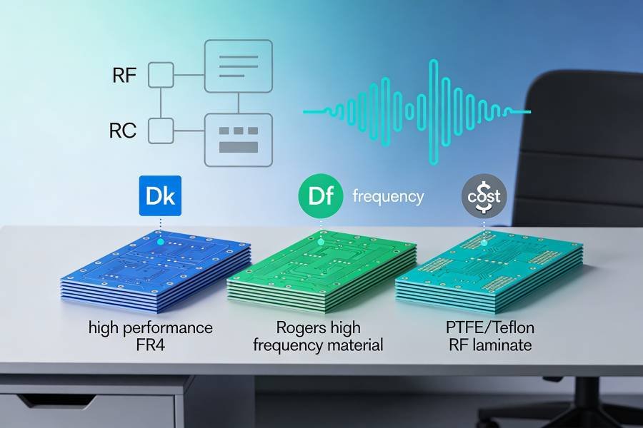
As RF and digital content keep moving onto the same board, “all‑FR4” and “all‑Rogers” designs each hit their limits. FR4 struggles with loss, impedance control, and stability at multi‑GHz frequencies, while building the entire stack on Rogers or other RF laminates can be unnecessarily expensive and harder to fabricate at scale. Hybrid high frequency PCBs solve this by combining Rogers (or similar RF materials) only where they are really needed—on critical RF and high‑speed layers—while using FR4 for digital logic, control, and power distribution in the rest of the stack.
In a typical hybrid Rogers+FR4 design, the RF layers carry low‑loss microstrip or coplanar lines over a well‑characterized dielectric, and the inner FR4 layers handle dense routing, connectors, and power planes at much lower material cost. This approach is now common in 5G base station modules, Wi‑Fi 6/7 routers, automotive radar, and satellite communication hardware, where demanding RF front‑ends live next to complex digital SoCs and power circuitry on a single PCB. In the rest of this article, we will look at when a hybrid Rogers+FR4 stackup makes sense, how typical layer structures are arranged, and what layout and manufacturing details you need to get right so RF and digital sections work together reliably instead of fighting each other.
What Is a Rogers + FR4 Hybrid PCB?
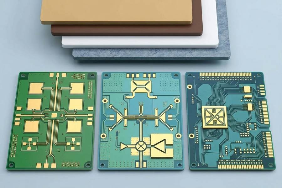
A Rogers + FR4 hybrid PCB is a multilayer board that intentionally mixes two laminate families in one stackup: high‑frequency Rogers material on the RF‑critical layers and standard (or high‑performance) FR4 on the remaining layers. In a typical construction, one or more Rogers cores (for example RO4350B or RO4835) carry microstrip or coplanar RF traces and are bonded together and to FR4 cores using FR4 or dedicated bondply/prepreg, while FR4 layers handle digital signals, power planes, and mechanical stiffness.
The key idea is to put low‑loss, well‑controlled Dk material only where it directly affects RF performance, instead of building the entire PCB from expensive RF laminates. This hybrid build‑up optimizes insertion loss and impedance accuracy on the RF layers, while FR4 provides lower cost, good availability, and robust mechanical properties for dense digital routing and connectors. Done correctly, a Rogers/FR4 hybrid stackup can reduce material cost by 40–60% compared to an all‑Rogers board, while still meeting the RF requirements of applications like 5G base station antennas, automotive radar, and mixed RF/digital modules.
If you are looking for a manufacturing partner that already builds these kinds of hybrid RF and digital boards, our high‑frequency PCB fabrication services can help.
When to Choose a Hybrid Rogers + FR4 Design
Hybrid Rogers+FR4 designs make the most sense when only part of your board truly needs RF‑grade performance, and the rest looks like a conventional digital or mixed‑signal design. If your critical RF circuits live mainly on one or two outer layers—antennas, power amplifiers, LNAs, filters, or high‑speed SerDes lanes—while inner layers carry MCUs, FPGAs, control interfaces, and power rails, a hybrid stackup lets you put Rogers only under those RF layers and keep FR4 everywhere else. This is especially attractive when FR4’s loss and Dk variation would hurt RF performance, but building the entire stack on Rogers would overshoot the budget.
You will see Rogers+FR4 hybrids widely used in 5G base station and small‑cell radios, Wi‑Fi 6/7 access points, automotive radar front‑ends, IoT gateways with RF modules plus processors, and satellite communication or phased‑array boards where RF and digital live side by side. In these systems, the RF front‑end and antenna feed networks demand low‑loss, stable Dk to hit link budgets and beam‑forming accuracy, while the digital and power sections mainly care about routability, cost, and mechanical robustness—exactly the split that hybrid stackups address. On the other hand, if almost every layer carries high‑frequency or ultra‑tight‑tolerance signals, or the environment is extreme enough that you need uniform RF material throughout (for example certain aerospace or mmWave radar designs), an all‑Rogers or all‑PTFE solution may still be the better fit.
We routinely manufacture Rogers+FR4 hybrid PCBs for 5G radios, Wi‑Fi, radar, and mixed RF/digital modules, and can help you decide whether a hybrid stackup or a full RF build is more appropriate for your design.
Typical Rogers + FR4 Hybrid Stackup Patterns
Hybrid Rogers+FR4 designs tend to fall into a few repeatable stackup patterns, each balancing RF performance, routing space, and cost in a slightly different way.
Pattern 1: Top RF layer on Rogers, inner layers on FR4 (4‑layer example)
A very common structure for 1–6 GHz designs is:
- L1: Rogers RF signal (microstrip or CPWG)
- L2: FR4 ground plane
- L3: FR4 power / digital signals
- L4: FR4 digital / connectors
Here, only the top core is Rogers (for low‑loss RF routing), while the rest of the board is FR4. This works well when most RF activity is on the top side—antennas, PAs, LNAs, filters—and the inner/bottom layers mainly support digital logic and power distribution.
Pattern 2: Symmetric RF‑on‑both‑sides hybrid (4–6+ layers)
For dual‑side RF or better mechanical balance, designers often place Rogers on both outer layers and FR4 in the middle:
- L1: Rogers RF signal
- L2: FR4 ground / power
- L3…L(n‑2): FR4 digital / power
- L(n‑1): FR4 ground
- L(n): Rogers RF signal
The Rogers outer layers carry RF feeds or antennas, while FR4 inner layers route dense digital and power; symmetry helps control bow/twist and improves reliability through thermal cycling. This pattern shows up in base‑station antenna modules and radar front‑ends where both sides of the PCB are used for RF structures.
Pattern 3: Locally embedded RF sub‑board in an FR4 main board
In more advanced designs, a small Rogers “RF island” is milled and embedded into a cutout in a larger FR4 board, then laminated together. The RF sub‑board can itself be multilayer (for example a 4–6 layer RO4350B stack) carrying antennas and RF routing, while the FR4 host board provides connectors, digital routing, and mechanical support around it. This local hybrid lamination dramatically reduces RF material usage—often by more than half—while still giving the RF section the dedicated stackup it needs.
Across all these patterns, the common theme is that RF signal layers live on Rogers, tightly referenced to nearby ground planes, while FR4 layers carry digital, control, and power where loss and Dk variation are less critical. The exact choice between “simple RF‑on‑top,” “symmetric RF‑both‑sides,” or “embedded RF sub‑board” depends mainly on how much RF area you need, how many digital layers you must support, and how aggressive your cost and reliability targets are.
Key Design Considerations for RF–Digital Integration on Hybrid Boards
On a Rogers+FR4 hybrid PCB, you are not just mixing materials—you are integrating two very different “worlds” (RF and digital) in one mechanical and electrical structure. Getting the details right on layer assignment, vias, grounding, and partitioning is what turns a hybrid stackup from a cost‑saving idea into a reliably performing product.
First, group your layers by function and sensitivity. RF signal layers should sit on Rogers with an adjacent solid ground plane, while FR4 layers can carry digital signals, power, and low‑frequency nets. Keep RF traces on the Rogers layers whenever possible, and avoid dropping them deep into FR4 where loss and Dk variation are higher. Use the FR4 inner layers for wide power planes and dense digital routing, but ensure that any high‑speed digital interfaces still see a controlled‑impedance environment with proper reference planes.
Via transitions deserve extra care because they often cross material boundaries. When an RF via moves a signal from a Rogers outer layer into an inner FR4 layer or back, the dielectric constant and physical thickness change, which can alter impedance if the via and pads are not designed accordingly. Minimize such transitions on critical RF paths; when they are unavoidable, model them with appropriate drill size, pad/antipad, and nearby ground returns, and consider using blind/buried vias or backdrilling to control stubs in thicker hybrid builds. Around the interface between Rogers and FR4 regions, add dense ground stitching vias so return currents see a continuous, low‑impedance path and mechanical stresses from differing CTEs are better distributed.
Finally, think about RF–digital partitioning in both floorplan and routing. Place RF blocks over the Rogers zones with clear keep‑outs around them, keep noisy digital and switching power circuits over FR4 zones, and avoid routing digital clocks or fast edges directly beneath sensitive RF lines—even if they are on FR4—without adequate shielding and spacing. Use ground “moats,” via fences, and where necessary metal shields to isolate RF from digital, and ensure that any intentional crossings (for example control lines into an RF front‑end) are short, well‑decoupled, and referenced to a solid ground plane. With these considerations baked into the design, a Rogers+FR4 hybrid board can behave like a coherent system rather than two unrelated PCBs laminated together.
Manufacturing Challenges and How to Work with Your Fabricator
Hybrid Rogers+FR4 boards are powerful but not “business as usual” for manufacturing; they introduce extra variables in lamination, drilling, and reliability that you and your fabricator must manage together. The main challenges come from CTE and Tg mismatches between RF laminates and FR4, different resin flow behaviours during lamination, and the need to hold tight impedance and flatness tolerances across dissimilar materials.
The first issue is thermal expansion and lamination. High‑frequency materials like many Rogers grades typically have different coefficients of thermal expansion and curing requirements than standard FR4, so if you simply stack them together like ordinary cores, you can end up with warpage, voids, or even layer‑to‑layer delamination after lamination or multiple reflow cycles. To mitigate this, fabricators often pair RF laminates with high‑Tg, low‑CTE FR4, choose compatible prepregs or dedicated bondplies at the Rogers–FR4 interface, and fine‑tune press temperature, pressure, and cool‑down profiles. A symmetric stackup and balanced copper distribution further help keep bow and twist under control in production.
Because these knobs live on the manufacturing side, early collaboration with an experienced hybrid‑capable fabricator is essential. The practical workflow is: you propose a target stackup (materials, thickness, layer count, impedance goals), then your fab reviews it and responds with a buildable hybrid structure, including specific laminate part numbers, bondplies, and the impedance data they can guarantee. From there, you base all impedance rules, RF routing, and via modelling on that confirmed stackup, and include clear notes in your documentation—calling out hybrid materials, impedance‑controlled nets, and any special via or backdrill requirements. Treating your fabricator as a design partner from day one turns hybrid Rogers+FR4 lamination from a reliability risk into a repeatable process that supports both RF performance and volume yield.
Our RF and hybrid PCB manufacturing team can review your proposed stackup, material choices, and impedance targets and suggest a buildable hybrid structure before you commit to layout.
Example Use Case: A Simple Rogers + FR4 Hybrid for an RF Front‑End + MCU
Consider a compact 4‑layer board that combines a 2.4/5 GHz RF front‑end with a microcontroller and power management in a single PCB. A practical hybrid stackup might use Rogers RO4350B for the RF outer layer and high‑Tg FR4 for the inner and bottom layers, similar to many real‑world “0.98 mm RO4350B+FR‑4” hybrid builds used for RF/digital integration.
One example stackup looks like this:
- L1: 35 μm copper on 0.508 mm RO4350B core – RF signal layer (antennas, PA/LNA, filters)
- L2: 18 μm copper on FR4 prepreg – solid ground plane (reference for L1 RF and L3 digital)
- L3: 18 μm copper on FR4 core – digital signals, MCU, control, and power distribution
- L4: 35 μm copper – FR4 bottom layer for connectors, low‑speed I/O, and optional shielding copper
In this design, all RF routing—antenna feeds, matching networks, low‑loss microstrip or CPWG traces—stays on L1 over the RO4350B core, referenced to the solid ground plane on L2 for clean 50 Ω control and low insertion loss. The MCU, SPI/I²C interfaces, GPIOs, and DC‑DC converter live mostly on L3 and L4 in FR4, where loss is much less critical and routing density matters more than dielectric performance. RF‑to‑digital control lines (for example enable pins, SPI to an RF front‑end IC) cross between regions quickly and are referenced to ground on L2 to avoid injecting digital noise into the RF section.
From a manufacturing perspective, the fabricator pairs the RO4350B core with a compatible high‑Tg FR4 and uses an appropriate prepreg or bondply to laminate them into a rigid 0.98 mm board. Impedance‑controlled coupons for the 50 Ω RF lines are added on the panel so that the shop can verify line performance during production, while standard FR4 processes are used for drilling, plating, and ENIG finish across the hybrid stack. The result is a board that meets the RF loss and impedance requirements on L1, provides ample digital and power routing on L3/L4, and costs significantly less than an all‑Rogers design of the same complexity.
Conclusion
Hybrid Rogers+FR4 PCBs exist to give you RF performance where it matters and FR4 economics where it does not. By putting critical RF layers on Rogers with solid nearby ground planes, and using FR4 for digital, control, and power routing, you can hit multi‑GHz loss and impedance targets without paying for an all‑Rogers stackup.
The key to making this reliable is disciplined engineering and close cooperation with a hybrid‑capable fabricator: choose compatible materials, design a symmetric, well‑referenced stackup, control via transitions across materials, and partition RF and digital sections thoughtfully. When you treat the stackup, RF–digital integration, and lamination process as a single problem, a Rogers+FR4 hybrid board becomes a very practical default option for many modern RF‑plus‑digital products.
When you are ready to move from a hybrid stackup concept to real hardware, you can send us your files and requirements—our Rogers and FR4 hybrid high‑frequency PCB fabrication and assembly services cover everything from prototypes to production.