Table of Contents
Why High‑Speed vs High‑Frequency PCB Confuses So Many Engineers
In everyday conversations, engineers often use “high‑speed PCB” and “high‑frequency PCB” as if they meant the same thing, but they actually describe two different design worlds. High‑speed boards are all about fast digital edges and time‑domain signal integrity, while high‑frequency boards focus on analog RF behavior at GHz‑range carrier frequencies. The distinction matters, because each type pushes you toward different materials, stackups, layout rules, test methods, and even manufacturing partners.
If you treat a high‑speed SerDes backplane like an RF front‑end, you may over‑specify exotic laminates and processes and drive costs up unnecessarily; if you treat a 5G RF module like a generic high‑speed digital board, you risk excessive loss, detuned matching networks, and inconsistent performance in production. This article breaks down what “high‑speed” and “high‑frequency” really mean in PCB design, compares their design goals and rules side by side, and shows how to choose the right materials, layout strategies, and PCB manufacturer when your next project falls into one camp—or straddles both.
Definitions: What Is “High‑Speed” and What Is “High‑Frequency” PCB Design?
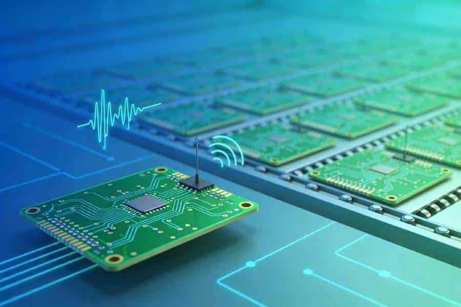
In the industry, “high‑speed” and “high‑frequency” both describe designs where PCB physics strongly affect signal behavior, but they refer to different kinds of signals and analysis. High‑speed PCB design is usually defined as digital designs where the rise/fall time of logic edges is short enough that traces behave as transmission lines, so signal integrity depends on layout, stackup, and impedance control rather than just schematic topology. Rules of thumb often classify a board as high‑speed when edge rates are in the 1–2 ns range or faster, when trace lengths approach more than about one‑sixth of the signal’s wavelength, or when fundamental frequencies exceed roughly 50–100 MHz, though the exact cutoff depends on the application.
High‑frequency PCB design, by contrast, deals with analog RF, microwave, and millimeter‑wave signals where the carrier itself is in the hundreds of megahertz to multi‑gigahertz range. Many sources treat boards carrying signals above about 500 MHz to 1 GHz as high‑frequency PCBs, with common application ranges extending from a few gigahertz up to tens or even hundreds of gigahertz in advanced radar and mmWave systems. Instead of focusing on digital timing, high‑frequency design focuses on frequency‑domain behavior—S‑parameters, impedance and VSWR, insertion and return loss, phase and group delay, and radiation from antennas or other RF structures. In short, high‑speed PCBs are about moving bits with clean edges in time, while high‑frequency PCBs are about guiding electromagnetic waves with predictable behavior in frequency.
Signal Types and Frequency Ranges
High‑speed and high‑frequency PCBs both deal with signals that are sensitive to layout and materials, but the underlying signal types are different. High‑speed designs carry digital signals—square‑like waveforms representing 1s and 0s—where the important parameter is the edge rate (rise/fall time) rather than the nominal clock frequency; these edges contain harmonics that extend well into the hundreds of megahertz or low gigahertz, even if the base clock is much lower. In this domain, you worry about reflections, overshoot, crosstalk, jitter, and timing margins on interfaces such as DDR, PCIe, Ethernet, and SerDes links.
High‑frequency PCB designs instead carry continuous‑wave or modulated RF signals where the carrier itself sits at high frequency, typically from around 500 MHz or 1 GHz up into the microwave and mmWave bands. Common examples include Wi‑Fi, Bluetooth, GNSS, cellular (sub‑6 GHz and 5G NR FR1/FR2), radar, and other RF front‑ends, where performance is characterized in terms of S‑parameters, impedance and VSWR, insertion and return loss, phase and group delay, and radiation patterns. In practical terms, you might call a design “high‑speed” when fast digital interfaces dominate and “high‑frequency” when RF carriers above about 1 GHz are the main concern, but many modern systems—such as 5G base stations or advanced ADAS radar ECUs—are firmly in both camps at once.
Design Goals: Digital Signal Integrity vs Analog RF Performance
Although both high‑speed and high‑frequency PCBs require controlled impedance and careful layout, their primary design goals are not the same. In high‑speed digital design, the focus is on time‑domain signal integrity: ensuring that logic transitions arrive at receivers with adequate amplitude, clean edges, low jitter, and within tight timing windows relative to clocks and other signals. Engineers worry about reflections, ringing, overshoot/undershoot, crosstalk, eye‑diagram opening, and skew across parallel or differential interfaces; success is often measured in unit‑interval margins and bit‑error rates rather than absolute gain or phase.
High‑frequency PCB design, in contrast, is fundamentally a frequency‑domain problem. Here the goal is to guide RF energy with predictable impedance, low loss, and controlled phase through transmission lines, filters, couplers, matching networks, and antennas. Key figures of merit include S‑parameters (S11, S21, etc.), voltage standing‑wave ratio (VSWR), insertion and return loss, group delay, and radiation efficiency or pattern shape; even small variations in line geometry, dielectric constant, or copper roughness can shift center frequency or degrade Q‑factor. Put simply, high‑speed designers primarily care that digital bits are distinguishable and synchronized in time, while high‑frequency designers care that RF waves maintain their amplitude, phase, and spectral characteristics as they pass through the PCB.
Materials and Stackups for High‑Speed vs High‑Frequency PCBs
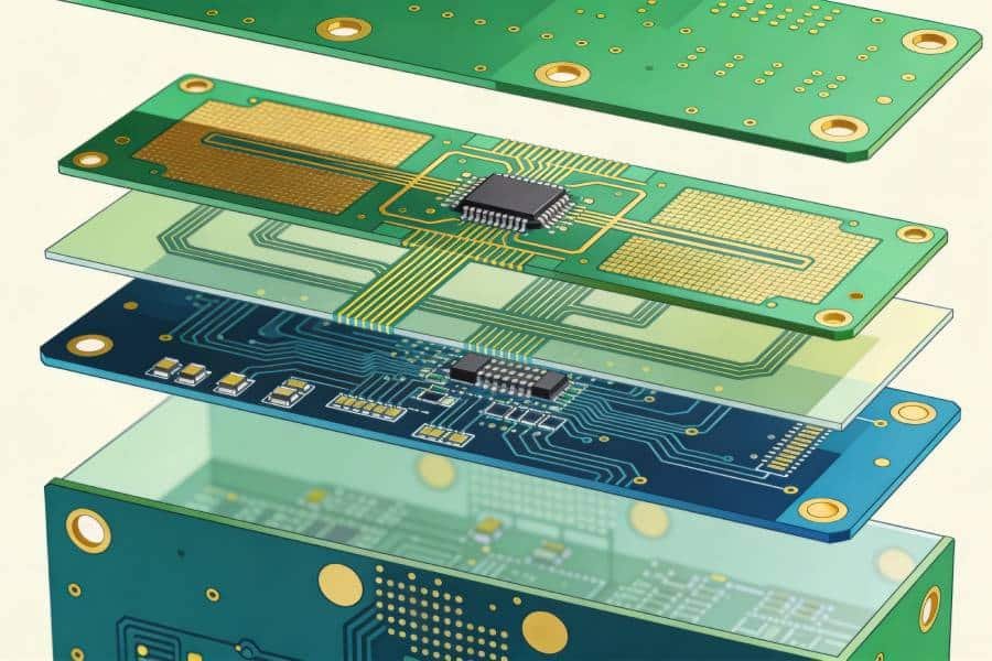
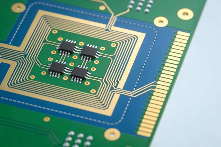
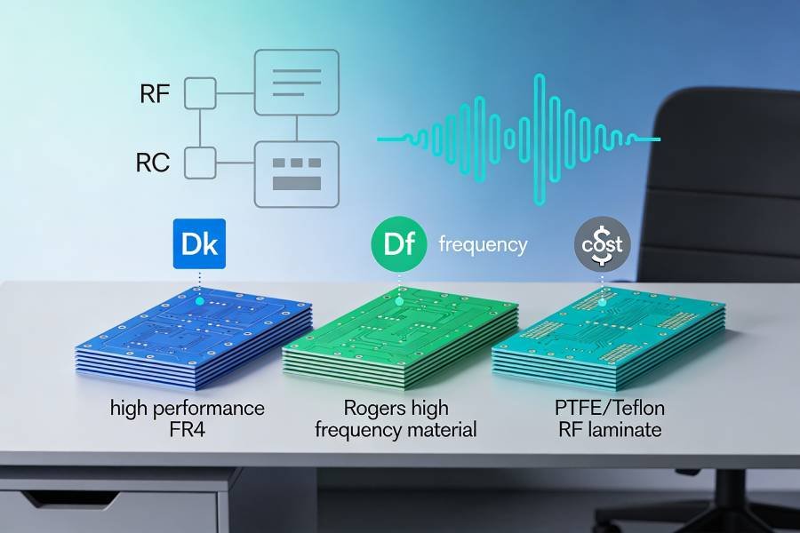
High‑speed and high‑frequency designs both care about dielectric properties, but they push you toward different material choices and stackup priorities. In high‑speed digital boards, the main concerns are loss and dispersion along long interconnects; many designs use enhanced or low‑loss FR‑4 materials (for example high‑Tg FR‑4, low‑loss FR‑4, or mid‑grade hydrocarbon laminates) that offer a reasonable balance of dielectric constant stability, dissipation factor, cost, and manufacturability up into the low‑GHz range. Stackups are often optimized to support dense routing with multiple reference planes, controlled impedance for a variety of single‑ended and differential traces, and acceptable skew and delay across wide buses.
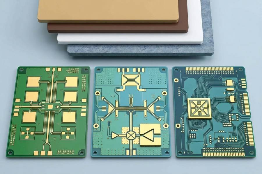
High‑frequency PCBs, especially in RF, microwave, and mmWave applications, typically demand materials with lower and more tightly controlled Dk and Df than standard FR‑4 can provide. Designers frequently turn to dedicated RF laminates such as Rogers RO4000/RO3000 series, PTFE‑based composites, or ceramic‑filled substrates, which minimize insertion loss and phase variation over frequency and temperature but come at higher material and processing cost. Stackups in high‑frequency boards tend to prioritize clean transmission‑line structures (microstrip, stripline, grounded coplanar waveguide), solid and continuous ground planes under RF paths, carefully controlled dielectric thicknesses, and, in many cases, hybrid constructions where RF layers sit on low‑loss laminates while digital or power layers use FR‑4 to manage overall cost.
Layout and Routing Rules: What Really Differs
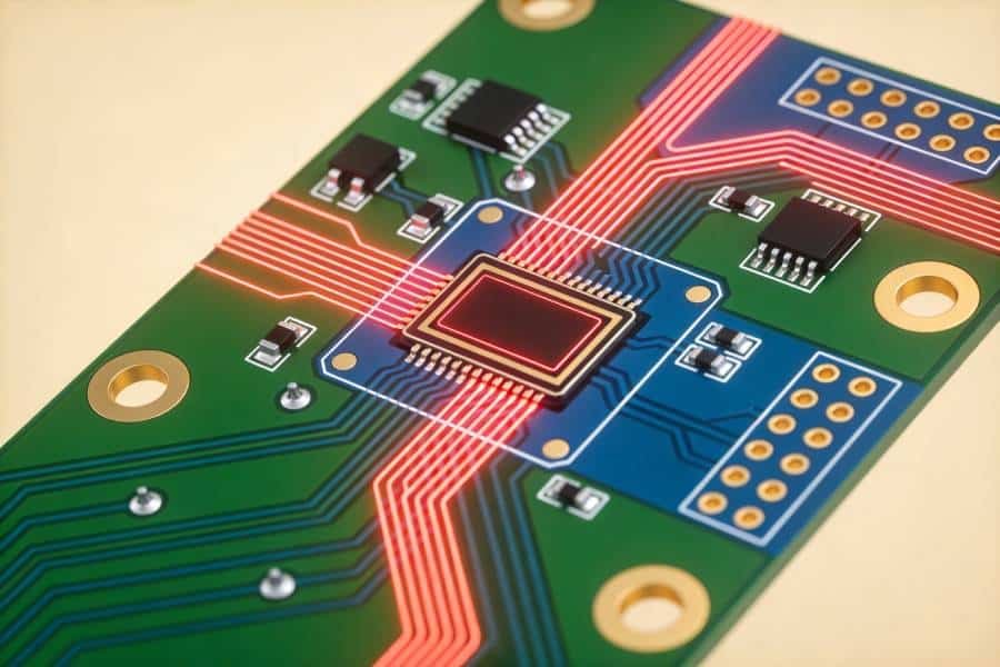
In layout rules, the most visible difference between high-speed and high-frequency boards is what you optimize for: timing coordination versus controlled energy transmission paths. High-speed digital design prioritizes length matching for buses and differential pairs to control skew, keep signals within timing budgets, and preserve eye diagrams at the receiver. Typical rules include tightly controlled impedance, minimizing via count on critical nets, avoiding long parallel runs that increase crosstalk, and always providing continuous, unbroken reference planes beneath high-speed traces to ensure predictable return paths and reduce EMI.
High-frequency RF and microwave routing, on the other hand, is closer to “sculpting transmission lines” than simply drawing interconnects. Designers focus on well-defined transmission-line structures such as microstrip, stripline, and grounded coplanar waveguide, keeping traces as short and straight as possible, and replacing right-angle corners with 45-degree bends or arcs to avoid impedance discontinuities and excess radiation. RF traces are usually surrounded by dense via fences and solid ground regions to confine fields, and designers avoid crossing plane splits or making unnecessary layer transitions, since each via, discontinuity, or plane change introduces extra inductance, capacitance, and potential radiation that show up directly in S-parameters, return loss, and gain. In short, high-speed routing is about getting bits to arrive cleanly and on time, while high-frequency routing is about guiding electromagnetic waves along precisely defined structures with minimal reflection, loss, or leakage.
Typical Applications and Example Scenarios
High-speed PCBs are widely used wherever large volumes of digital data need to move quickly and reliably between ICs, boards, or system modules. Typical applications include servers and data center equipment, high-performance computing and AI accelerators, networking switches and routers, storage systems, and high-end consumer devices such as smartphones, game consoles, and laptops. In these systems, interfaces like DDR memory, PCIe, Ethernet, HDMI, DisplayPort, USB, and various SerDes links define the high-speed requirements and drive constraints on routing density, timing, and signal integrity.
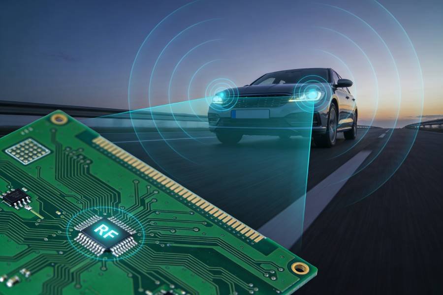
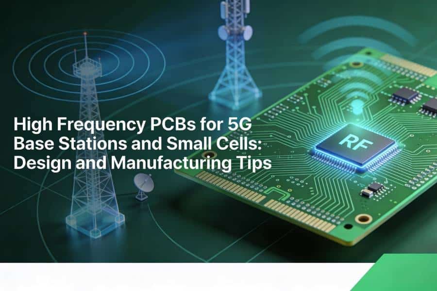
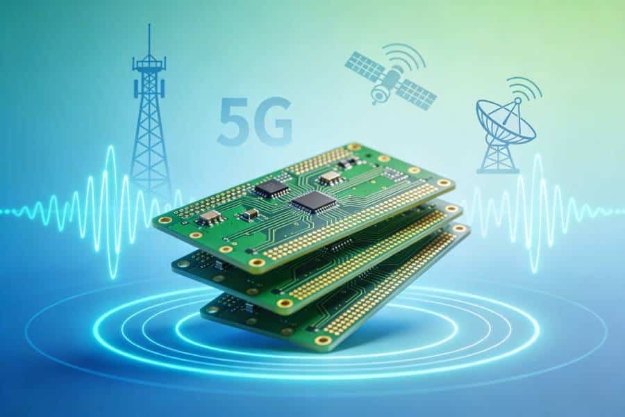
High-frequency PCBs, in contrast, show up wherever RF energy at hundreds of megahertz to tens of gigahertz must be generated, filtered, transmitted, or received. Common examples include 5G base stations and small cells, RF front-ends in smartphones and IoT devices, Wi‑Fi and Bluetooth modules, satellite communication terminals, radar systems, and microwave sensors used in automotive ADAS, industrial sensing, aerospace, and defense. These boards often contain power amplifiers, LNAs, mixers, filters, couplers, and antennas implemented directly in the PCB, making low loss, stable impedance, and tightly controlled layout essential to meeting link budget and regulatory requirements.
Many real products combine both high-speed and high-frequency requirements in a single design, which is where the distinction becomes practically important. A 5G base station, for instance, may use high-speed backplane links, high-bandwidth digital beamforming, and fronthaul interfaces alongside multi-band RF transceivers and phased-array antenna panels on the same or closely coupled PCBs. Similarly, a modern automotive radar control unit integrates high-frequency radar front-ends operating at 77 GHz with high-speed processors, memories, and in-vehicle network interfaces such as Ethernet or PCIe, forcing designers to partition stackups, materials, and layout rules according to whether a given region is dominated by digital high-speed or analog RF behavior.
If you need a manufacturing partner for real‑world high‑frequency RF boards, you can turn to our dedicated high frequency PCB manufacturer with Rogers, PTFE and hybrid stackups from 500 MHz up to 20 GHz.
When Designs Are Both High‑Speed and High‑Frequency
In many modern systems, the same PCB must handle high‑speed digital signals and high‑frequency RF or microwave signals at the same time. Examples include 5G base stations, wireless routers, smartphone RF front‑ends, satellite terminals, and mixed‑signal industrial or automotive control units where fast processors and interfaces sit near sensitive RF sections. In these designs, you cannot treat the board as “just high‑speed” or “just RF”; instead, you must deliberately partition the layout, stackup, and grounding strategy so that each domain gets what it needs without polluting the other.
The first key strategy is functional and physical segregation: place high‑speed digital, high‑frequency RF, and noisy power‑conversion circuits in clearly defined zones, with short, well‑controlled interfaces between them. Use dedicated reference planes and, where necessary, split or partially isolated ground regions that connect at controlled points rather than allowing arbitrary overlapping of digital and RF return currents. Route high‑speed digital signals on layers and in regions that avoid coupling into RF transmission lines, and keep clocks, PLLs, and SerDes links away from antennas, LNAs, and other noise‑sensitive RF nodes.
The second strategy is to treat via transitions, layer changes, and plane crossings as RF structures wherever they touch high‑frequency paths or very fast digital channels. Carefully designed via transitions with stitching vias, optimized antipads, and continuous return paths allow both RF and multi‑gigahertz digital signals to cross layers with minimal reflection and radiation. At the same time, maintaining consistent impedance, minimizing stubs, and avoiding hatched or heavily slotted planes under critical routes helps keep both S‑parameters (for RF) and eye diagrams (for digital) within specification.
Choosing the Right Manufacturer and Process for Each Type
For high-speed digital PCBs, you need a manufacturer that can reliably hold impedance, layer registration, and via quality on dense multilayer boards, but you can often stay within enhanced FR‑4 or mid‑loss materials. Important capabilities include controlled-impedance fabrication with test coupons, consistent trace width/spacing at fine geometries, HDI options (microvias, via‑in‑pad) for dense BGA breakouts, and solid DFM support to review stackups and routing for signal‑integrity risks before production. For prototypes and low volumes, quick‑turn services that offer at least basic impedance control and a range of low‑loss FR‑4 or Megtron‑class laminates are usually sufficient, as long as they provide clear stackup data, material specs, and test reports.
For high-frequency RF and microwave PCBs, you should specifically look for a shop with proven experience in PTFE and RF laminates, hybrid Rogers + FR‑4 constructions, and tight impedance control over a wide frequency range. Key indicators are: an inventory of major RF materials (Rogers, Taconic, Isola, ceramic‑filled PTFE), specialized drilling and plasma processes for PTFE, low‑profile copper handling, and the ability to hit impedance within about ±5% with documented S‑parameter or VNA testing when needed. For high‑power or very high‑frequency designs (radar, 5G, satellite), also check that the manufacturer supports metal‑backed or thick‑copper RF boards, controlled‑depth drilling, backdrilling to remove stubs, and has reference projects or certifications in aerospace, defense, or telecom RF applications.
When a design is both high-speed and high-frequency, the best choice is a manufacturer that explicitly advertises mixed digital‑RF capability and hybrid stackups, not just generic multilayer or RF work. Such partners can help you define stackups that place RF paths on low‑loss laminates and digital layers on FR‑4, advise on via structures and backdrill plans that work for both SerDes and RF launches, and tune the process window so that both eye diagrams and RF S‑parameters meet target specifications in volume. Spending time early with their CAM/engineering team to review your layout, materials, and test strategy typically pays off by reducing re‑spins and avoiding subtle performance shifts between prototype and mass production.
For RF and microwave designs, it is important to work with a specialist high frequency PCB manufacturer that already has experience with Rogers, PTFE and hybrid RF + FR4 stackups.
Summary Table: High‑Speed PCB vs High‑Frequency PCB
| Aspect | High‑Speed PCB | High‑Frequency PCB |
|---|---|---|
| Main signal type | Digital signals with fast edges and discrete logic levels. | Analog RF, microwave, or mmWave signals (continuous‑wave or modulated). |
| Typical frequency range | Edge harmonics extending into hundreds of MHz to a few GHz; clock/data rates often from hundreds of Mbps to tens of Gbps. | Carrier frequencies from roughly 500 MHz up to tens of GHz and beyond. |
| Primary design goal | Maintain digital signal integrity and timing margins (eye diagram, jitter, skew, crosstalk). | Control RF impedance, loss, and phase for good S‑parameters, VSWR, and radiation behavior. |
| Key figures of merit | Eye opening, BER, timing skew, jitter, crosstalk, impedance discontinuity. | S11/S21, return and insertion loss, phase stability, Q‑factor, noise figure, radiation pattern. |
| Typical materials | Enhanced or low‑loss FR‑4, modified FR‑4, mid‑loss hydrocarbon laminates. | RF laminates such as Rogers, PTFE‑based or ceramic‑filled substrates with very low Df and stable Dk. |
| Stackup focus | Multilayer with multiple reference planes, dense routing, differential pairs, length matching. | Clean transmission‑line structures, solid ground planes, controlled dielectric thickness, possible hybrid RF+FR‑4 stackups. |
| Layout and routing focus | Length‑matched buses, tightly coupled differential pairs, minimized vias, controlled return paths, reduced crosstalk. | Precisely dimensioned microstrip/stripline/coplanar lines, short and straight traces, gentle bends, via fences, and shielding. |
| Sensitivity to tolerances | Moderate to high sensitivity: impedance, skew, and loss must stay within budgets but often have some margin. | Very high sensitivity: small geometry or material shifts can detune filters, antennas, and RF paths. |
| Typical applications | Servers, data centers, AI accelerators, networking gear, high‑end consumer and automotive digital systems. | 5G/6G radios, Wi‑Fi/Bluetooth, radar, satellite links, RF front‑ends, microwave sensors. |
| Manufacturing priorities | Good controlled‑impedance capability, fine‑line routing, HDI, consistent via drilling/plating, strong SI‑oriented DFM. | Proven RF material handling, tight impedance control (often ±5%), RF test capability (e.g., VNA), experience with PTFE and hybrid stackups. |
FAQ: High‑Speed PCB vs High‑Frequency PCB
A PCB is typically considered high‑speed when the signal rise/fall times are short enough that interconnects behave like transmission lines, often when edge rates are in the sub‑nanosecond to a few‑nanosecond range and data rates reach hundreds of Mbps or higher.
A PCB is usually called high‑frequency when it carries analog RF or microwave signals with carrier frequencies above roughly 500 MHz to 1 GHz, extending into multi‑gigahertz and mmWave bands.
High‑speed PCBs focus on preserving digital signal integrity and timing (eye diagram, jitter, skew), while high‑frequency PCBs focus on analog RF performance such as S‑parameters, return loss, insertion loss, and phase stability.
Yes, both high‑speed and high‑frequency designs require controlled impedance, but high‑speed designs often emphasize differential impedance and timing, whereas high‑frequency designs emphasize very accurate single‑ended characteristic impedance and low loss over frequency.
Standard FR‑4 is generally not recommended for higher RF and microwave frequencies because of its higher dielectric loss and less stable dielectric constant, which increase insertion loss and detuning; specialized RF laminates such as Rogers or PTFE‑based materials are preferred.
Yes, many modern products (for example 5G radios, Wi‑Fi routers, and automotive radar units) combine fast digital interfaces with RF front‑ends, so the same system—or even the same PCB—must meet both high‑speed and high‑frequency design requirements.
You should separate digital, RF, and power sections into distinct physical zones, provide well‑defined reference planes and controlled ground connections, and keep noisy clocks and SerDes lines away from sensitive RF nodes and antennas.
Typical high‑speed PCB applications include servers and data‑center equipment, high‑performance computing and AI accelerators, telecom and networking gear, storage systems, and high‑end consumer or automotive digital platforms.
High‑frequency PCBs are commonly used in 5G and cellular infrastructure, RF front‑ends in phones and IoT devices, Wi‑Fi and Bluetooth modules, radar systems, satellite communication equipment, and microwave sensors.
Look for a fabricator with proven RF experience, access to major RF materials (Rogers, Taconic, PTFE, ceramic‑filled), tight impedance‑control capability (often ±5%), and RF test options such as VNA‑based S‑parameter measurements, plus a track record in telecom, radar, or aerospace projects.
If your next project involves RF, microwave, or mixed high‑speed + RF design, you can get a fast quote and DFM feedback from our high frequency PCB manufacturing services here.