Table of Contents
Why RF PCB Design Feels Different
At low frequencies, a PCB is mostly a convenient way to connect pins together. At RF and high‑frequency, the PCB itself becomes part of the circuit: every trace is a transmission line, every via is an inductor, and every gap or pad edge adds parasitics that can detune your carefully designed network. That is why RF PCB layout and manufacturing cannot be treated as “just another digital board” with a few routing constraints sprinkled on top.
Modern RF products make this even more challenging. Wireless modules, 5G small cells, radar front‑ends, IoT radios, and mixed‑signal SoCs pack sensitive RF paths next to noisy digital logic and power converters on increasingly dense boards. At the same time, higher operating frequencies and wider bandwidths mean tighter loss budgets, stricter impedance control, and less tolerance for layout “artwork” that used to be good enough. Good performance now depends as much on stackup, routing, grounding, and manufacturability as it does on the schematic itself.
This article focuses on practical RF PCB design guidelines for high‑frequency circuits, from early stackup planning through layout and into fabrication and assembly. Instead of treating each topic in isolation, we will walk the full path an RF signal sees on the board—through transmission lines, vias, grounds, and matching networks—and highlight concrete layout and manufacturing decisions that make first prototypes behave much closer to your simulations.
If you need a manufacturing partner who can actually build these high‑frequency RF designs, our high frequency PCB fabrication and assembly services can help.
Stackup and Material Planning: Build the RF Foundation
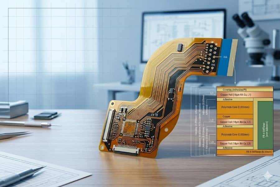
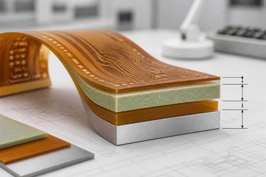
A good RF PCB starts with a good stackup; everything you do later with routing, grounding, and shielding depends on how signal, ground, and power layers are arranged and what materials you choose. At high frequencies, the stackup controls impedance, loss, isolation, and how predictable your transmission lines behave from simulation to production.
For most RF designs, you want each critical signal layer to sit directly next to a solid reference plane (usually ground) to simplify impedance control and give return currents a clean path. A typical high‑frequency multilayer might use outer microstrip layers over ground with inner stripline layers sandwiched between ground planes, while power planes sit close to ground to form tight decoupling capacitance. Thin dielectrics (for example 2–4 mil between RF signal and its reference plane) make it easier to hit 50 Ω with practical trace widths and reduce loss per unit length compared to thicker cores.
On the material side, the same trade‑offs you explored in the previous article still apply: FR4 is often fine for lower‑frequency or short RF runs, Rogers‑class materials give you lower loss and tighter Dk for many GHz designs, and PTFE‑based laminates come in when you push into very high frequency or ultra‑low‑loss territory. Hybrid stackups—RF layers in Rogers or PTFE, inner digital and power layers in FR4—are a practical way to get RF performance without over‑spending on the entire board, but they do require your fabricator to manage bonding, CTE mismatch, and lamination carefully. No matter which path you choose, you should finalize a realistic stackup with your PCB manufacturer early, using their actual laminate thicknesses and copper weights as the basis for all impedance calculations and EM simulations.
If you do not want to negotiate complex FR4/Rogers/PTFE stackups alone, you can involve our RF PCB engineering team early in your design to lock a buildable stackup before layout.
RF‑First Placement and Functional Partitioning
In RF PCB design, placement is not something you “clean up later” after routing; it is the first and most critical layout decision for high‑frequency performance. You should place the RF signal chain from input to output in a straight, compact path, then let digital logic, control, and power circuitry fill in around that backbone. Following the schematic order—antenna → filters → LNAs/PAs → mixers → IF/baseband—helps keep traces short, minimizes parasitics, and reduces the chance that outputs couple back into earlier, sensitive stages.
A good starting point is to partition the board into clear functional zones: RF, digital, and power. Keep high‑power RF blocks (like PAs) physically separated from low‑noise receive paths (like LNAs), ideally with their own local ground “corridors” and, where needed, metal shields. Place RF connectors (SMA, MMCX), antennas, and front‑end filters near the board edge to simplify routing and avoid snaking critical feedlines through noisy regions. Within each RF zone, keep matching networks and filters tight and symmetric—avoid stretching π or L networks across large distances, because “component‑to‑component trace” quickly becomes a non‑negligible part of the circuit at high frequency.
As you place components, think about fields and return currents, not just footprints. Inductors and transformers should be oriented to minimize mutual coupling—often at right angles to each other—and oscillators should sit close to their IC clock pins with a clean ground underneath and away from strong digital or RF power currents. Avoid crowding RF parts with dense via fields or unrelated signals; a small amount of “wasted” blank PCB area around a sensitive RF node is often the cheapest isolation you can buy. If you design with these placement rules first, the later routing, grounding, and shielding steps become much more straightforward—and your board layout ends up looking like the RF block diagram you started from.
RF Transmission Line and Routing Guidelines
Once the stackup and placement are under control, routing the RF paths becomes about treating every critical trace as a transmission line, not just a “wire.” Impedance, length, bends, layer changes, and spacing all directly impact gain, matching, and noise performance at high frequency.
For most RF PCBs you will use microstrip (outer layer over a solid ground plane), stripline (inner layer between two planes), or grounded coplanar waveguide (CPWG) with via fences. Microstrip is easy to access and tune; stripline offers better shielding and more consistent impedance; CPWG gives strong confinement and isolation between nearby lines when combined with a stitched ground “fence.” Whatever you choose, set up controlled‑impedance rules (often 50 Ω single‑ended for RF) based on your confirmed stackup and stick to them for all critical runs.
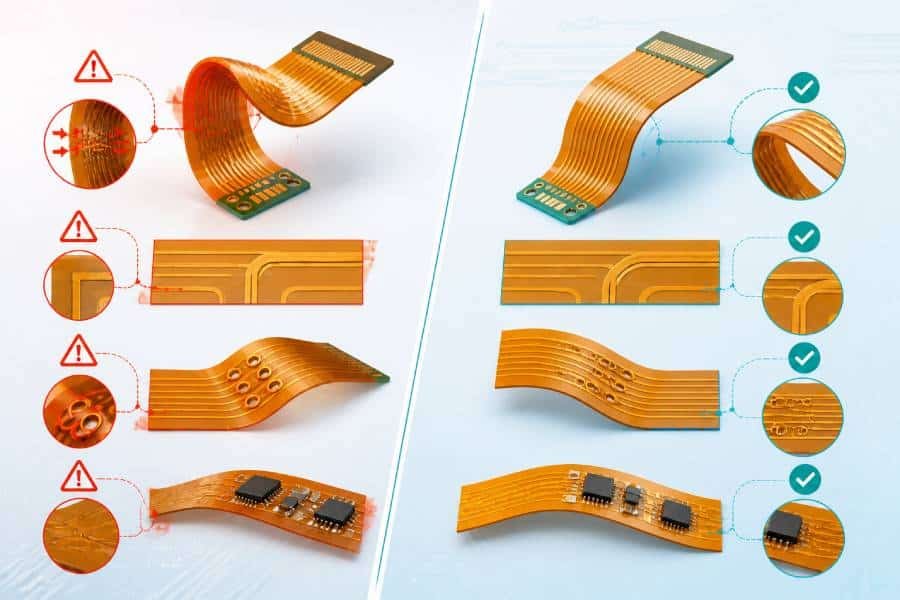
Keep RF traces as short, straight, and direct as possible, and avoid unnecessary layer changes. When you must bend a high‑frequency line, use shallow 45° segments or smooth curves rather than sharp 90° corners; if a right‑angle is unavoidable, use a properly mitered corner to compensate for the local impedance bump. Do not route RF lines in long parallel runs next to each other or next to noisy high‑speed digital; increase spacing, use CPWG with ground pours, or add grounded guard traces with stitching vias to control coupling and crosstalk.
Vias deserve special attention in RF routing because every via is a small inductive element and, if it leaves a stub, a resonant structure. Minimize via transitions on critical RF paths; when layer changes are unavoidable, keep the number of vias low, use tight antipads, and place one or more ground return vias very close to each signal via to preserve reference continuity. In thicker or high‑frequency boards, consider backdrilling to remove unused via stubs, or use blind/buried vias in HDI stackups to keep RF vias as short and non‑resonant as practical. By combining disciplined transmission‑line geometry, careful bends, and well‑engineered via transitions, you greatly increase the odds that your real‑world RF traces behave like the ideal lines you simulated.
Grounding and Return Paths: Give RF Currents a Way Home
In RF PCB design, you do not just route signals; you route loops. Every RF trace needs a clean, low‑impedance return path, usually in the adjacent ground plane, or its fields will spread, radiate, and couple into everything nearby. At high frequency, return current follows the path of least impedance directly under the trace, not the shortest physical distance, which is why continuous reference planes under RF lines are so important.
The first rule is to provide solid, unbroken ground planes directly beneath RF signal layers and avoid routing RF traces across any slots, splits, cutouts, or mixed power/ground areas. If a trace crosses a gap in its reference plane, the return current must detour around the opening, dramatically increasing loop area, inductance, and EMI. In mixed‑signal RF boards, modern practice favors a unified ground plane with careful functional partitioning and routing, instead of physically split analog/RF/digital grounds that are hard to manage at high frequency.
Stitching vias tie this ground system together. Whenever a signal changes layers, place at least one nearby ground via to give the return current a direct way to follow the signal between reference planes. Around RF zones, board edges, and coplanar RF lines, use rows of closely spaced ground vias (“via fences”) to confine fields and improve isolation; common guidance is to keep via spacing on the order of one‑twentieth of the shortest wavelength of interest, or just a few millimeters at multi‑GHz. Combine this with disciplined decoupling—short, low‑inductance connections from supply pins to the nearest ground plane—to keep power return currents local and prevent them from sharing sensitive RF ground paths.
Matching Networks and Passive RF Structures
Matching networks and passive RF structures are where layout starts to look almost as important as the schematic. A π or L network that works perfectly in simulation can miss its target badly on the PCB if traces, pads, and vias add too much extra inductance or capacitance. The higher the frequency, the more your physical layout becomes part of the matching network, not just the place you drop components.
For lumped matching networks (L, π, T), keep the components packed tightly together and close to the device or antenna port they are matching, with very short, direct traces between pads. Place series and shunt elements in the same order and orientation as in the schematic—do not “stretch” the network across the board, or the interconnects will behave like unintended transmission lines. Use high‑Q RF capacitors and inductors with self‑resonant frequencies well above your operating band, and give them a solid, low‑inductance ground underneath for shunt components. Around sensitive filters (for example SAW/BAW devices), follow the vendor’s recommended land patterns and layout notes closely, including keep‑outs, via fences, and ESD protection placement.
Printed passive structures—such as PCB filters, couplers, and baluns—add another layer of layout sensitivity. They rely on tight coupling, symmetry, and precise impedance, so any asymmetry in trace width, spacing, or ground referencing directly shows up as amplitude or phase imbalance. Keep coupled lines the same length and width, maintain constant spacing, and avoid abrupt changes in reference plane under these elements. It is often wise to include small “tuning stubs” or extra component pads (for example, a series resistor or shunt capacitor position) at the input and output of critical networks so that you can trim the match on real hardware without a full respin. Combined with good EM simulation of the whole network—including components, pads, and interconnects—this layout discipline makes it much more likely that your first build will land close to the S‑parameters you designed for.
Design for Manufacturing: Getting RF PCBs Built Right
Even a beautifully laid‑out RF PCB can disappoint if it is hard to fabricate, sensitive to process variation, or poorly documented for your manufacturer. Design for manufacturing (DFM) brings practical fab limits—trace width, spacing, drill sizes, stackup tolerances—into your RF decisions so the board can be built reliably and repeatably. At high frequency, small deviations in dielectric thickness, copper weight, or etch geometry directly affect impedance and loss, so RF designs tend to be less forgiving of DFM shortcuts than low‑frequency boards.
Start by aligning materials, stackup, and controlled‑impedance requirements with your chosen PCB house before you lock the design. Confirm which FR4, Rogers, or PTFE laminates they stock, what dielectric thicknesses and copper weights are standard, and what their minimum trace, spacing, and drill sizes look like for RF work. If you use hybrid stackups, make sure the RF and FR4 materials have compatible CTEs and that the fab has experience bonding those specific combinations. Include impedance‑controlled lines in your fab notes and work with your fabricator to add test coupons on the panel for each critical impedance so they can verify performance with TDR before boards ship.
On the documentation side, clean, unambiguous manufacturing data is part of RF DFM. Provide Gerber/ODB++/IPC‑2581 data, netlist, BOM, and clear fabrication and assembly drawings that call out stackup, materials, impedance targets, controlled‑depth drills or backdrilling, special via fills, and any RF‑specific keep‑outs or mask openings. Avoid over‑tightening DFM rules everywhere just because RF sections need special treatment; instead, constrain only the RF areas and allow standard manufacturability rules on the rest of the board so the job fits your manufacturer’s normal process as much as possible. This balance—RF performance where it matters, standard DFM elsewhere—helps you get high‑frequency behavior that matches your design without driving up cost and lead time unnecessarily.
If you would like a second set of eyes on your stackup, impedance constraints, or RF DFM rules before release, you can send us your Gerber and requirements and our high‑frequency PCB team will review them for manufacturability.
Validation and Tuning: Closing the Loop on the Bench
High‑frequency PCB work is never “done” at layout; the real test is how your board behaves on the bench. A good validation plan uses the same concepts you designed for—impedance, S‑parameters, and return paths—to check whether the fabricated PCB matches your expectations. That means planning access for measurements early, not trying to bolt on test points after the fact.
For RF paths, vector network analyzer (VNA) measurements of S‑parameters are the primary tool to validate gain, loss, and matching across frequency. Give yourself coax connectors or well‑defined launch structures at key ports, and keep the launches as close as practical to the networks you want to characterize to avoid long, unknown feedlines. Calibration and de‑embedding matter: use appropriate calibration (SOLT, TRL, or vendor‑recommended methods) and, where possible, design simple calibration/verification structures on the same PCB so you can separate board effects from your device behavior.
Beyond RF ports, basic design‑for‑test features make bring‑up and tuning much easier. Add accessible test pads or untented vias on supply rails, control signals, and representative transmission lines so you can probe voltages, clocks, and impedance with minimal loading. Leave a few optional component positions in critical matching networks (for example extra shunt pads to ground) so you can tweak the match or add damping resistors without cutting traces, and document a simple tuning plan in your lab notes before the first boards arrive. With these hooks in place, your RF PCB design is not just theoretically sound—it is also practical to measure, understand, and iterate when reality inevitably differs a little from simulation.
When you are ready to turn your RF layout into hardware, our high‑frequency RF PCB fabrication and assembly services can help you go from prototype to volume with the same design rules used in this guide.