Table of Contents
Moving a high frequency PCB from prototype to production is much more than simply ordering a larger batch of the same board. RF PCB prototyping and manufacturing involve specialized materials, tight impedance and loss targets, and more complex test strategies, so small decisions made during the first few samples can dramatically impact yield, reliability, and unit cost when you scale. Issues that are easy to workaround on the bench—like slight impedance drift, marginal insertion loss, or layout tweaks done by hand—can become major problems when you are building hundreds or thousands of boards per month.
For teams working on 5G radios, radar modules, wireless infrastructure, or high‑speed digital links, it is critical to think about “prototype to production” as a single, continuous process rather than two separate projects. That means aligning materials, stackups, RF test methods, and documentation from the first prototypes onward, while planning clear transition steps such as engineering validation and pilot runs. In this article, we will walk through each stage of the high frequency PCB prototype‑to‑production journey and highlight practical guidelines you can use to de‑risk your next RF ramp‑up, from the first proof‑of‑concept boards to stable, repeatable volume manufacturing.
In this guide we focus on the engineering side, but if you need a manufacturing partner who can actually build these boards, you can learn more about our high frequency PCB manufacturing services.
Stage 1 – RF PCB Prototyping: Goals, Constraints, and Typical Flow
In the prototype phase, the main goal is to validate RF performance and core functionality, not to minimize cost or maximize yield. You are trying to answer questions like “Does this antenna or filter meet its S‑parameter targets?”, “Is the link budget realistic?”, and “Are there any major layout‑related issues such as unexpected resonances or coupling?”—often with only a handful of boards on the bench. This is why early RF PCB prototypes typically favor flexibility and speed: engineers may accept higher high frequency PCB prototype cost, use quick‑turn services, and keep panelization simple so they can iterate fast.
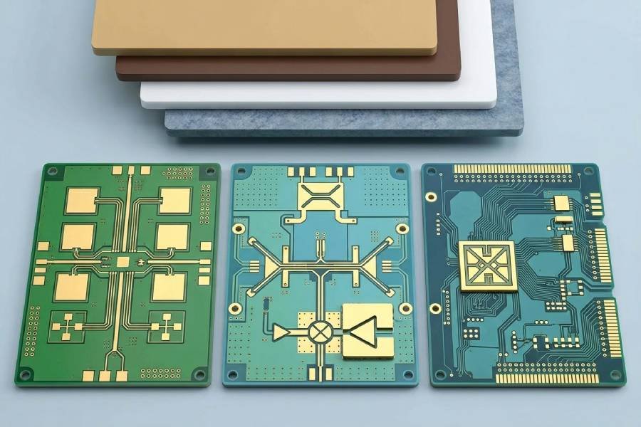
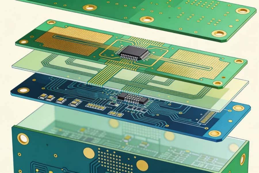
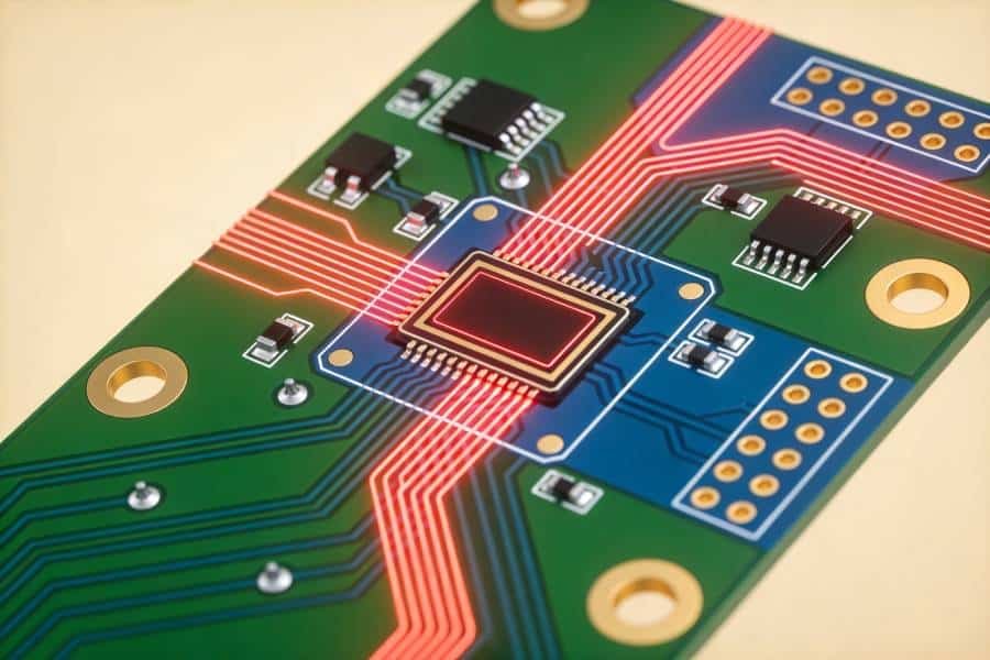
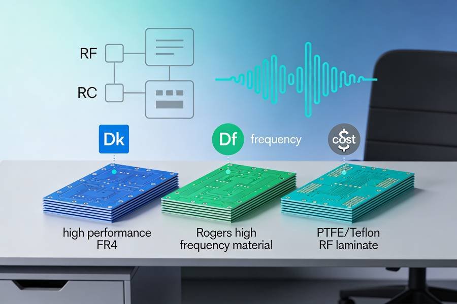
At the same time, RF PCB prototyping has some constraints that are very different from low‑frequency boards. You usually need to choose high frequency materials (such as Rogers, PTFE, or low‑loss FR‑4) and define at least a preliminary stackup that reflects your intended production build, because dielectric constant and loss have a direct impact on impedance, matching, and radiation efficiency. Layout precision also matters from day one: component placement, via transitions, ground returns, and length‑matching for differential or phased paths all influence the S‑parameters you measure on VNAs and other RF test equipment, so “rough” routing just to get a board made is rarely a good idea.
A typical RF PCB prototyping flow starts with a clear specification of frequency range, target impedances, and performance metrics, followed by simulation‑driven stackup and layout, then one or more quick‑turn prototype builds for lab validation. Early test campaigns usually prioritize a limited set of measurements—such as return loss, insertion loss, gain, noise figure, and key timing margins—so that design flaws can be identified and corrected quickly before the design is locked. Best practice is to keep the first prototypes as simple as possible (no unnecessary layers or features), document every design change and test result, and work closely with your RF PCB prototyping service to choose materials and options that resemble your eventual production plan while still supporting fast iteration.
Stage 2 – Engineering Validation: Refining Stackup, Materials, and RF Performance
Once the first RF PCB prototypes are on the bench and you have initial S‑parameter and functional results, the next step is engineering validation: turning promising prototypes into a design that is ready to scale. At this stage, the focus shifts from “does it roughly work?” to “does it still work across corners, and can we build it repeatably?”. That means correlating simulation and measurement, tightening or relaxing key constraints, and deciding whether your chosen materials and stackup are really the right fit for performance, reliability, and manufacturability.
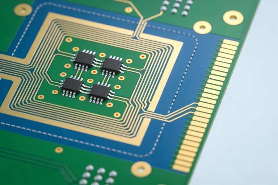
A typical high frequency PCB engineering‑validation loop starts by analyzing discrepancies between expected and measured behavior. You compare lab data—return loss, insertion loss, group delay, noise figure, linearity, and so on—against EM and circuit simulations, then work with your PCB fabricator to identify whether deviations are caused by material properties (real‑world Dk/Df vs. datasheet), manufacturing tolerances (trace width, dielectric thickness, copper roughness, via stubs), or layout issues such as coupling and resonance. In many RF programs, this is also when dedicated validation coupons or test vehicles are built using the same stackup and processes as the main board, so you can characterize materials and interconnects more precisely and feed that data back into your models.
Based on these findings, you refine the design and the manufacturing recipe together. On the design side, that might mean adjusting trace geometries, via structures, stitching strategies, or matching networks to achieve better correlation and margin; on the manufacturing side, it can involve fine‑tuning stackup targets, etch compensation, drill sizes, plating thickness, and press cycles to bring impedance and loss into a stable, repeatable window. You also begin to define a more robust test strategy for later stages—deciding which RF parameters must be verified on every lot or sample, which electrical tests (for example TDR, flying probe, functional) are required, and what documentation or golden‑board references the factory will need when you move into pilot runs and early production. A well‑executed engineering validation phase greatly reduces surprises during NPI, because you enter pilot builds with a stackup, material set, and RF PCB manufacturing process that have already been proven to match your simulations and reliability expectations.
Stage 3 – Pilot Runs and NPI for High Frequency PCB Manufacturing
In high frequency projects, pilot runs are the bridge between “nice lab results” and a manufacturable RF product. Instead of building a handful of boards for validation, you deliberately run a small batch—often on the order of a few dozen to a couple of hundred units—using the same materials, stackup, and RF PCB manufacturing processes you expect for production. The goal is to verify not just RF performance, but also process stability, assembly yields, and test coverage under realistic factory conditions, so you can fix problems while the risk and cost are still manageable.
A well‑structured NPI pilot for high frequency PCBs typically includes several elements. On the fabrication side, you confirm that drilling, plating, lamination, impedance control, and any special RF processes (such as backdrilling or plasma treatment) meet their targets across the entire batch, then review yield data, scrap reasons, and coupon/test results with the factory. On the assembly and test side, you exercise the full RF test plan—whether that is flying‑probe plus functional RF tests, or more advanced S‑parameter and performance checks—and look for systemic issues like tuning drift, marginal solder joints around RF components, or sensitivity to reflow profiles. The outcome of Stage 3 should be a set of controlled, documented process parameters and design tweaks that give you confidence the design can move into volume with predictable high frequency behavior, acceptable yields, and no last‑minute surprises.
Once your RF design is stable, working with a single high frequency PCB prototype to production partner helps keep stackups, materials, and test methods consistent from the first samples to mass production.
Stage 4 – Scaling to Volume: Process Control, Yield, and Cost Stability
When a high frequency PCB moves into volume manufacturing, the primary challenge shifts from “Can we build this?” to “Can we build thousands of these consistently at a predictable cost?”. At this point, small variations in material properties, trace geometry, via quality, or assembly conditions that were invisible in prototype quantities can start to erode yield, causing scrap, rework, and RF performance drift across lots. For RF and mmWave designs in particular, maintaining stable impedance, insertion loss, and phase behavior over large panel counts requires tighter process capability (for example Cpk targets on dielectric thickness, copper thickness, line width, and drill position) and more disciplined in‑line monitoring than standard FR‑4 production.
Scaling successfully therefore depends on robust process control and data‑driven yield management. Mature RF PCB manufacturers define clear process windows for each critical step—lamination, drilling, plating, imaging, etching, solder mask, and final finishes—and then use SPC charts, AOI/X‑ray statistics, impedance coupon results, and RF test data to track how each batch behaves relative to those windows. When you review this data with your supplier, you are looking for trends rather than isolated defects: gradual shifts in impedance, loss, or assembly yield often indicate that a process is drifting and needs corrective action before it affects field performance. By locking down the validated stackup, DFM rules, and test strategy from earlier stages—and insisting on documented control plans and regular yield reviews—you can turn what was once a fragile RF prototype into a stable, repeatable high frequency PCB product with predictable cost and quality at volume.
Design Considerations That Change from Prototype to Production in RF PCBs
As you move from RF prototypes to production, the design priorities subtly shift from maximum flexibility and “getting it to work” toward manufacturability, repeatability, and cost. Layout patterns, stackups, and tolerances that are acceptable on a handful of boards may not survive the variability of high‑volume high frequency PCB manufacturing. Understanding which design choices need to tighten, and which can safely relax, is key to a smooth high frequency PCB prototype‑to‑production transition.
The first area that typically evolves is geometry and tolerances. Early RF prototypes may use aggressive line widths, spacing, and via structures to squeeze functionality into limited space or to explore performance extremes, but for production you often standardize on more uniform trace geometries, via styles, and copper distribution that your fabricator can hold with high Cpk across large panels. You may also adjust impedance and phase‑matching tolerances—tightening them where testing shows margins are thin, and relaxing them where you have comfortable headroom—to balance RF robustness with yield. Grounding, shielding, and partitioning usually become more systematic as well, with clearer zoning between RF, digital, and power regions to reduce sensitivity to normal process and assembly variation.
The second big shift is DFM and documentation. Prototypes can sometimes tolerate ad‑hoc fabrication notes, manual rework, or informal test setups, but production RF PCBs require fully specified stackups, controlled impedance targets, clear drill and solder mask tables, and unambiguous fabrication and assembly drawings. You also need to design footprints, test pads, and access points that support automated inspection and test, such as AOI, X‑ray, flying probe, or functional RF fixtures, rather than relying on bench probes alone. Finally, component choices (for example RF amplifiers, filters, and matching passives) often get revisited with supply‑chain and derating in mind, so that your design can survive lifecycle changes and still meet RF performance when built by different lots and lines over time.
Practical Tips to De‑Risk High Frequency PCB Prototype to Production Transitions
To de‑risk a high frequency PCB prototype‑to‑production journey, it helps to treat manufacturability and scalability as first‑class requirements from the very first revision. Start by defining a clear RF specification—frequency range, target impedances, loss budgets, and key performance metrics—and keep that spec tightly linked to your stackup and material choices as the design evolves. Even during early RF PCB prototyping, run at least a basic DFM review with your manufacturer so that obvious manufacturing red flags (over‑tight geometries, non‑standard thicknesses, hard‑to‑solder footprints) are caught before they become baked into a design that will later need to scale.
As you approach engineering validation and pilot runs, increase the rigor of your reviews and documentation. Use structured design‑review checklists that cover RF layout, impedance control, grounding, testability, and mechanical constraints, and make sure your fabrication and assembly drawings fully describe the intended high frequency PCB manufacturing process. Plan at least one pre‑production build whose purpose is explicitly to stress the process: monitor yields, review scrap codes, and compare RF measurements across multiple panels and lots to ensure the design behaves consistently under real‑world variation. Finally, capture what you learn—preferred stackups, stable design rules, proven test strategies—and reuse these “known good” patterns in future RF PCB prototyping and manufacturing cycles so that each new product starts from a lower‑risk, production‑ready baseline instead of reinventing everything from scratch.
FAQ – High Frequency PCB Prototype to Production
For most high frequency designs, it is wise to run at least two prototype spins: an initial proof‑of‑concept build and a refined engineering‑validation build that already uses your intended materials and stackup. Once the second spin shows good correlation between simulation and measurement and passes basic environmental and functional tests, you can plan a pilot run in the range of a few dozen to a few hundred boards to validate manufacturing yields and RF performance under realistic factory conditions.
You do not always need to use the exact production laminate and thickness in the very first prototype, but you should match dielectric type and Dk/Df class as closely as possible so your RF behavior scales correctly. By the engineering‑validation stage, it is strongly recommended to switch to the actual high frequency materials and stackup you plan to use in production, otherwise you risk discovering different impedance and loss characteristics only after you start ramping volume.
The most effective approach is to treat pilot runs and NPI as mandatory steps, not optional extras: run a controlled small batch using production processes, then review yield data, RF measurements, and failure modes with your manufacturer before committing to large orders. Combine this with robust DFM reviews, stable design rules, and a documented test strategy (including impedance and key RF checks), and you can greatly reduce surprises in high frequency PCB manufacturing as you move from prototype to production.
Summary Checklist – High Frequency PCB Prototype to Production
You can use this short checklist as a final sanity check before each major step in your high frequency PCB prototype‑to‑production journey.
- Requirements locked: Are frequency range, impedance targets, loss budgets, and key RF metrics clearly documented and shared with your PCB manufacturer?
- Materials and stackup: By engineering validation, are you using the same (or equivalent) high frequency materials and stackup that you plan to run in production?
- DFM/DFT reviews: Have you completed at least one joint DFM/DFT review with your RF PCB supplier covering layout rules, test access, panelization, and assembly constraints?
- Correlation and margin: Do lab measurements from prototypes correlate with simulations, and is there sufficient margin across expected process and environmental corners?
- Pilot build executed: Have you run a defined pilot batch (dozens to hundreds of boards) using production processes and reviewed fabrication, assembly, and RF yield data?
- Process controls in place: Are critical process parameters (lamination, drilling, plating, impedance, RF tests) documented with clear control limits and monitoring plans for volume?
- Release package ready: Do you have a complete, version‑controlled release package including Gerbers/ODB++, stackup, drill tables, fab and assembly drawings, BOM, test procedures, and acceptance criteria?
If you are ready to discuss your next RF project, you can send your design files directly through our High Frequency PCB Manufacturer | RF & Microwave PCB Fabrication page.