Table of Contents
5G macro base stations and small cells look very different on the outside, but inside they share the same challenge: packing high‑frequency RF, high‑speed digital, and power circuitry onto dense multilayer PCBs that must run reliably for years in the field. As operating bands move from legacy sub‑GHz into Sub‑6 and FR2/mmWave ranges, traditional “FR‑4 only” boards quickly run into limits on loss, impedance control, isolation, and thermal performance. Getting the stackup, materials, RF layout, and manufacturing process right is no longer a “nice to have” optimization—it is what determines whether a 5G radio actually meets its link budget, EVM, and lifetime targets once it leaves the lab.
In this article, we focus specifically on high frequency PCBs for 5G base stations and small cells rather than generic RF design theory. You will see how to choose sensible material tiers for Sub‑6 and FR2, plan stackups that separate RF and high‑speed digital, apply practical RF layout and antenna‑integration tips, and account for thermal and DFM constraints from day one. The goal is not to replace detailed simulation or vendor datasheets, but to give you a concrete checklist you can use with your PCB manufacturer when turning a 5G concept into production‑ready hardware.
If you need a manufacturing partner who can turn these design rules into reliable hardware, our high frequency PCB fabrication services for 5G infrastructure support Rogers, PTFE, and hybrid stackups from quick prototypes to volume production.
5G System Overview: Macro Base Stations vs Small Cells
5G macro base stations and small cells implement the same basic radio chain—RF front‑end, transceiver, baseband, and power—but the way these blocks land on the PCB is quite different. Macrocells prioritize high power, multi‑sector coverage, and robustness in harsh outdoor sites, while small cells focus on compact size, lower transmit power, and cost‑effective high‑volume manufacturing for dense urban or indoor deployments.
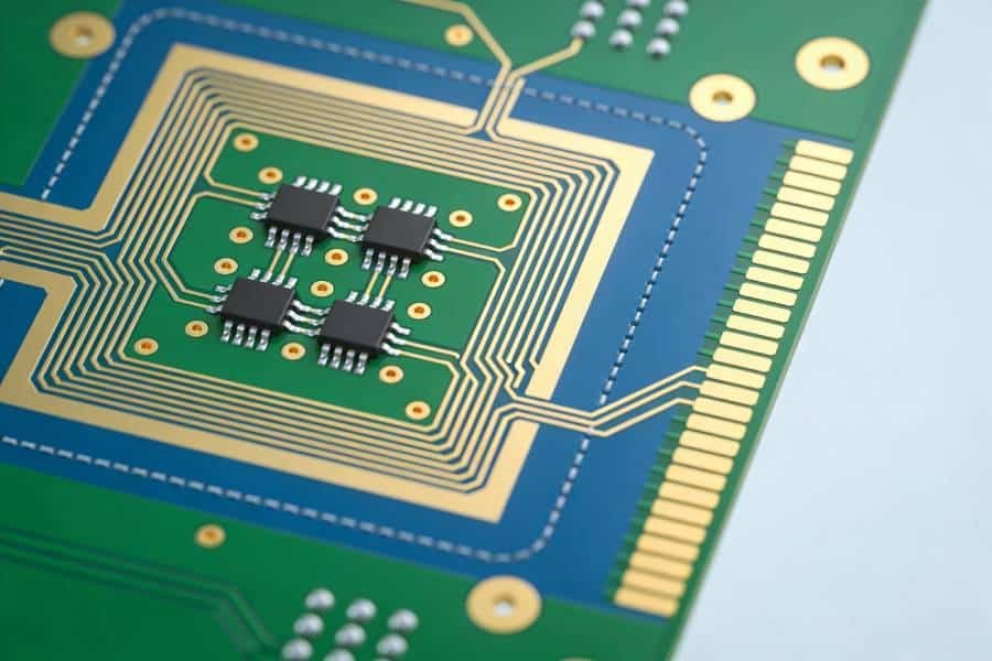
In both cases, high frequency PCBs carry the RF front‑end and high‑speed interfaces that sit closest to the antennas. Typical RF sections include PAs, LNAs, filters, duplexers, phase shifters, beamforming ICs, and RF switches, all connected through controlled‑impedance transmission lines that must meet tight insertion‑loss and isolation budgets across one or more 5G bands. Around them, high‑speed digital baseband, clocking, and SERDES links share the same board or a closely coupled companion PCB, adding further constraints on layer stackups and routing density.
Macro base station radios often split functionality across multiple boards—for example, separate RF front‑end and high‑power amplifier modules, sometimes on hybrid PTFE/Rogers PCBs, plus digital baseband and power distribution boards on FR‑4 cores. Small cells, by contrast, frequently integrate RF, transceiver, baseband, and power management onto a single dense multilayer PCB or a compact RF module plus a main digital board, which pushes line/space, via technology, and thermal design much harder within a small footprint. Understanding where your design sits on this macro–small‑cell spectrum is the first step in deciding how aggressive you need to be with materials, stackup, and RF layout on your high frequency PCB.
Material Choices for 5G High Frequency PCBs
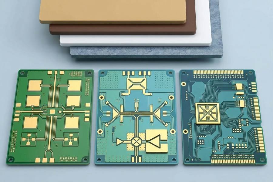
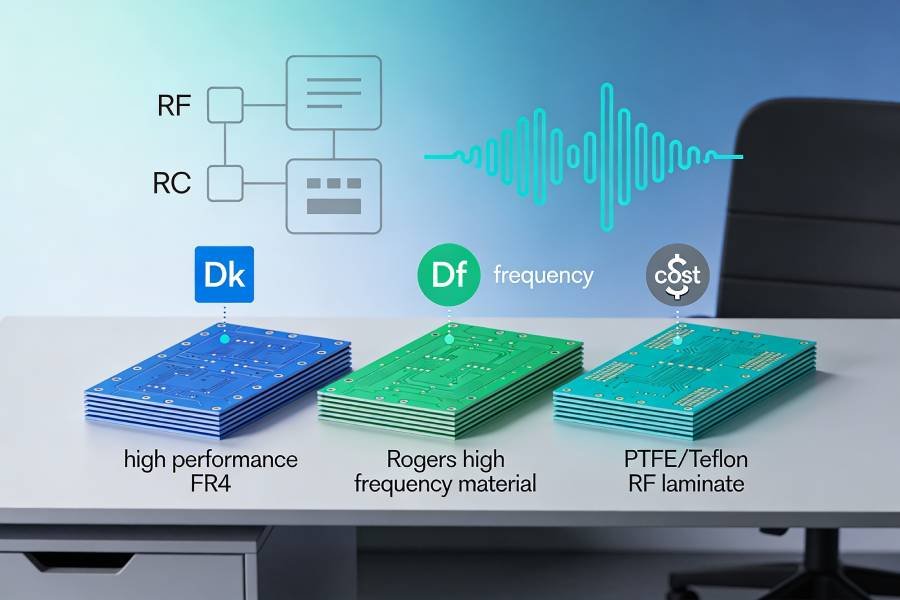
For 5G base stations and small cells, material selection usually starts with the operating band and then balances loss, stability, and manufacturing cost. Sub‑6 radios can often use high‑grade FR‑4 in non‑critical RF paths, but quickly benefit from Rogers‑class hydrocarbon/ceramic laminates on the key RF layers, while FR2/mmWave designs typically require PTFE‑based or very low‑loss Rogers materials throughout the RF section.
In Sub‑6 GHz macro base stations, a common pattern is a hybrid stackup: RO4350B or RO4003C on the antenna and RF front‑end layers, with high‑Tg, low‑loss FR‑4 for digital, control, and power planes, which keeps loss and impedance under control without paying for premium laminate across the entire board. Cost‑sensitive small cells running in the lower part of Sub‑6 may stretch FR‑4 a bit further by using enhanced low‑loss FR‑4 grades on short RF paths, but they still often adopt at least one Rogers layer near the antenna feed and PA/LNA to protect link budget and EVM.
Once you move into FR2/mmWave (typically 24–40 GHz), the material window narrows: low‑loss hydrocarbon/ceramic laminates like RO3003 or RO4003C and, for more demanding arrays, PTFE or ceramic‑filled PTFE become the default choices for RF feedlines, couplers, and antenna interfaces. These materials offer Dk in roughly the 3.0–3.4 range with Df well below 0.003 at 10 GHz, which is important for keeping attenuation manageable over beamforming networks and multi‑element antenna arrays. LCP and other advanced substrates sit at the very high‑end of this spectrum, mainly for tightly integrated or flexible RF modules, and are more common in user equipment than in large base station PCBs, but they can appear in compact small‑cell RF front‑end modules where size and integration are critical.
When you are ready to move from material short‑lists to a concrete, buildable stackup, our engineers can help you select practical laminates and thicknesses through our 5G high frequency PCB material and stackup review service.
Stackup and Layer Planning: Getting Impedance and Isolation Right
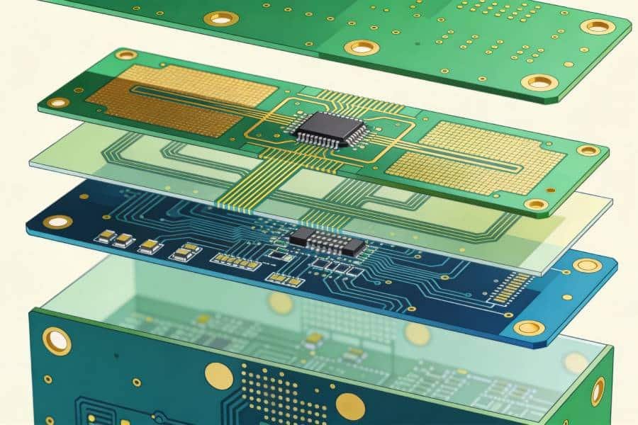
A good stackup is where high frequency PCB design for 5G base stations and small cells really starts to look different from ordinary digital boards. You are trying to keep RF paths low‑loss and well shielded, while routing dense high‑speed digital and power distribution in the same physical volume.
For most 5G infrastructure designs, four‑layer PCBs are too limited, and you quickly move into 8–12+ layer territory to separate RF, high‑speed digital, and power planes cleanly. A common pattern is to place primary RF layers on the outer surfaces as microstrip (for easier tuning, probing, and antenna feeding), each directly adjacent to an unbroken ground plane, while high‑speed digital and power planes live on inner layers with their own solid references. Every signal layer—RF or digital—should have a continuous reference plane directly above or below it to provide low‑inductance return paths and predictable impedance.
Hybrid stackups are especially attractive in 5G base stations: RF layers use Rogers‑class laminates while inner digital layers use FR‑4, with dedicated bondply between them. In a typical 10–12 layer base station design, you might see something like “RF signal – ground – high‑speed signal – power – digital signal – digital signal – power – high‑speed signal – ground – RF signal,” where the top and bottom RF layers are low‑loss material and the inner core is FR‑4. This kind of S‑G‑S‑P‑S‑S‑P‑S‑G‑S arrangement maintains symmetry, gives every signal layer a close reference, and keeps expensive laminate only where the RF needs it.
Two details often make or break 5G stackups: ground integrity and via strategy. Ground planes under RF sections should be as continuous as possible—no large slots, cutouts, or “islands”—because any break forces return currents to detour and can turn parts of the board into unintended antennas. Around critical RF traces and between RF and digital regions, dense via stitching and via fences tie ground layers together, improving shielding and reducing the risk that high‑frequency energy leaks into noisy digital or power areas.
If you share your target layer count and approximate board size, we can propose a 5G‑ready stackup and impedance plan that fits our high frequency PCB manufacturing capabilities and stocked materials.
RF Layout Tips for 5G Base Stations and Small Cells
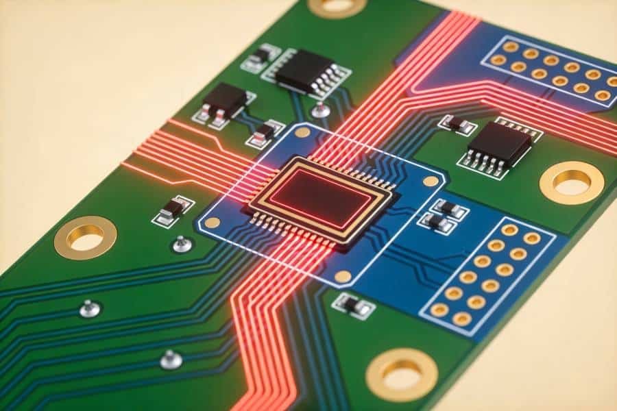
On 5G high frequency PCBs, RF layout is where many otherwise good stackups lose performance through unnecessary loss, mismatch, or coupling. The core goals are simple—keep RF paths short, predictable, and well shielded—but hitting them consistently requires discipline in how you route, place components, and treat vias.
For RF traces, route on outer layers over a solid ground plane, using controlled‑impedance microstrip or grounded coplanar waveguide, and avoid unnecessary layer changes. Keep feedlines between PAs, LNAs, filters, and antennas as short and straight as practical, and reserve space for matching networks (pi or T pads) near each critical interface so you can fine‑tune performance during bring‑up. When vias are unavoidable, treat each transition as a small RF structure: use back‑drilling or blind vias to remove stubs, add nearby ground vias to contain fields, and keep via fences along RF edges at roughly λ/20 spacing or better to improve isolation.
Antenna integration looks different between macro base stations and small cells, but the PCB rules are similar. Respect antenna keep‑out zones with no copper, vias, screws, or tall components in the near field; keep noisy digital and power circuits physically and electrically separated from the antenna feeds; and follow the antenna vendor’s reference layout closely, especially around ground patterns and matching structures. In compact small cell designs, place antennas or antenna‑in‑package modules at board edges or corners to maximize free‑space exposure and use ground pours plus via fences to block coupling into neighboring RF chains and high‑speed digital lanes.
Thermal Management and Power Integrity
5G base stations and small cells run dense RF and digital silicon at relatively high power densities, so thermal management on the PCB is not optional—it directly impacts RF linearity, lifetime, and even network uptime. The basic strategy is to create a low‑resistance thermal path from hot devices into copper planes, then out into heat spreaders, chassis, or external cooling solutions.
For high‑power PAs and beamforming ICs, place dense thermal via arrays directly under the exposed pad, tying into large internal or bottom copper areas that connect to heat sinks, metal baseplates, or the enclosure. Use thicker copper where needed (for example 2 oz on power layers) and consider hybrid designs where RF layers sit on low‑loss material while power sections use substrates with better thermal conductivity or even metal‑core or copper‑coin inserts in extreme cases. In compact, often fanless small cells, the PCB and enclosure effectively become the heat sink, so plan early how hot spots will couple through thermal interface materials into the chassis.
Power integrity is just as important as heat flow because noisy supplies can degrade phase noise, EVM, and receiver sensitivity. Keep power planes close to ground planes in the stackup to lower impedance, and place multiple decoupling capacitors of different values close to each RF and high‑speed IC power pin, with the smallest value physically closest. Route supply paths so current flows through the decoupling capacitors before it reaches the device, minimize vias in these critical loops, and use low‑ESR capacitors and short, wide traces to keep supply noise and voltage droop under control.
Manufacturing Considerations for 5G High Frequency PCBs
Compared with ordinary digital boards, 5G base station and small cell PCBs demand tighter control over materials, layer registration, via quality, and impedance than many factories are used to. You are typically working with high‑layer‑count stackups, hybrid laminates, fine lines, and HDI features, all of which must survive outdoor environments and long lifetimes without performance drift.
On the capability side, 5G infrastructure boards commonly use 10–16 or more layers, line/space down to 75–100 μm, and controlled impedance tolerances around ±5% on critical RF and high‑speed traces. HDI technologies such as laser‑drilled microvias, blind and buried vias, and via‑in‑pad are increasingly standard in small cells and compact RF modules to route dense beamforming and high‑speed interfaces within tight footprints. When you combine this with hybrid materials (Rogers + FR‑4), the fabricator must also manage different CTEs and lamination cycles so that the finished panel stays flat and within thickness tolerances.
Up front, good DFM practice for 5G high frequency PCBs means sharing your proposed stackup, materials, and RF constraints with the manufacturer before layout is frozen. Ask specifically about stocked laminate types and thicknesses, supported copper foils (for example HVLP or rolled for lower loss), maximum layer count, HDI structures they are comfortable with, and preferred surface finishes—ENIG or ENEPIG are usually better than HASL for fine‑pitch RF and high‑speed components. Finally, plan for manufacturing verification: impedance coupons, cross‑sections, and, for mmWave designs, S‑parameter testing on reference structures help ensure that the real boards behave close to your simulation models once they leave the factory.
Practical Checklist for 5G Base Station and Small Cell PCBs
To make all of this actionable, it helps to run each new design through a simple checklist that aligns RF, layout, and manufacturing decisions before you lock the PCB. The idea is not to cover every edge case, but to make sure the big, expensive mistakes are avoided early.
1. Define the scenario clearly
- What frequency bands are you targeting (Sub‑6, FR2/mmWave, or both)?
- Is this a macro base station radio, a compact small cell, or a shared RF module used in multiple products?
- What are the key performance metrics: output power, receiver sensitivity, EVM, bandwidth, and expected lifetime?
2. Choose a realistic material tier
- Sub‑6, moderate RF lengths: low‑loss FR‑4 plus Rogers‑class laminate on critical RF layers.
- FR2/mmWave, longer RF paths or arrays: low‑loss hydrocarbon/ceramic or PTFE for all RF layers, FR‑4 only for inner digital if a hybrid stackup is feasible.
- Confirm that your fabricator stocks the chosen materials and thicknesses at reasonable lead times.
3. Plan the stackup and layer roles
- Target at least 8–10 layers for serious 5G base station or small cell designs, with RF signal layers adjacent to solid ground planes.
- Allocate distinct “zones” for RF, high‑speed digital, and power, and sketch which layers each will occupy before detailed routing.
- Review the hybrid lamination (if used) with your PCB vendor to avoid warpage and lamination‑cycle issues.
4. Apply disciplined RF layout rules
- Keep RF paths short, straight, and on outer layers; minimize unnecessary via transitions.
- Use ground pours, via fences, and keep‑out regions to isolate RF from noisy digital and switching power stages.
- Follow antenna and RF IC reference layouts closely, especially around matching networks and ground patterns.
5. Address thermal and power integrity early
- Identify the hottest devices (PAs, beamforming ICs, DC‑DC converters) and give each a clear thermal path via via arrays into copper and then into the chassis or heat sinks.
- Design power planes and decoupling networks so that supply noise and droop stay within the RF vendors’ recommendations across temperature and load transients.
6. Close the loop with your manufacturer
- Before finalizing the layout, review the stackup, materials, HDI structures, and impedance requirements with your PCB fabricator.
- Ask for their standard impedance coupon structures and testing capabilities, especially if you are working above 10 GHz or into FR2 bands.
- Build at least one early prototype run with full fabrication reports (cross‑sections, impedance results) so you can tune models and layouts before volume.
Conclusion: From Design Rules to Reliable 5G Hardware
High frequency PCBs are one of the main reasons why 5G base stations and small cells are harder to build than previous‑generation radios: you are managing RF, high‑speed digital, power, and thermal constraints in the same tight stackup. The right combination of material, layer structure, RF layout discipline, and thermal and power‑integrity design often matters more for real‑world performance than squeezing another dB out of an individual component.
The practical way to approach these designs is to tie decisions back to a few fundamentals: your target bands and RF path lengths, realistic material tiers your manufacturer can supply, a stackup that gives every critical layer a clean reference plane, and early DFM reviews to align design assumptions with fabrication reality. When those pieces are in place, 5G macro base station and small cell PCBs move from being “exotic RF projects” to repeatable platforms you can evolve across product generations with less risk and rework.
When your 5G design is ready to leave the lab, you can rely on our end‑to‑end high frequency PCB manufacturing and assembly services for 5G base stations and small cells to bridge the gap from material selection and stackup, to RF‑proven production hardware.