Table of Contents
Modern ADAS depends heavily on automotive radar, from long‑range front radar for adaptive cruise control to corner and side radar for blind‑spot monitoring, lane changes, and parking assistance. Behind each of these sensors is an automotive radar PCB that has to carry 77–79 GHz RF circuitry, high‑speed digital links, and power delivery in a very small footprint, while surviving years of vibration, temperature swings, moisture, and contamination under the hood or behind bumpers. At these frequencies, a high frequency PCB for ADAS is no longer “just another multilayer board”—material choice, stackup, layout, and manufacturing discipline directly affect range, angular resolution, false‑alarm rates, and ultimately vehicle safety.
This article focuses on what makes an automotive radar PCB and high frequency PCB for ADAS different from standard designs, and what you can do about it as a hardware or layout engineer. We will walk through radar and ADAS basics, high‑frequency and automotive‑grade requirements, practical material and stackup options, layout and antenna‑integration guidelines, and the thermal and reliability considerations that matter in mass production. The goal is to give you a clear, engineering‑oriented checklist you can apply when working with your PCB manufacturer, so your next radar or ADAS design is not only high‑performing on the bench, but also robust on the road.
If you are looking for a manufacturing partner that understands both RF performance and automotive‑grade reliability, our high frequency PCB manufacturing services cover automotive radar PCBs and high frequency PCBs for ADAS, from material and stackup selection to mass production.
Automotive Radar and ADAS Basics
Automotive radar is the workhorse sensor in ADAS because it can directly measure distance, relative speed, and angle in almost any weather or lighting conditions. Modern vehicles typically use multiple radar modules around the car: long‑range radar at the front for adaptive cruise control and automatic emergency braking, mid‑range units for lane‑change assistance and cross‑traffic alerts, and short‑range radar at the corners and rear for blind‑spot monitoring and parking assistance.
Most current automotive radar systems operate in the 76–81 GHz band using FMCW (frequency‑modulated continuous‑wave) techniques, with 76–77 GHz often used for long‑range radar and 77–81 GHz providing wider bandwidth and higher resolution for short‑range and high‑definition sensing. From a PCB perspective, that means dealing with wavelengths on the order of only a few millimeters in air and roughly 1 mm in typical RF laminates, which makes transmission‑line geometry, stackup, and even small layout discontinuities critical for performance. As ADAS functions such as ACC, AEB, blind‑spot monitoring, and automated parking become standard across vehicle tiers, the number of radar modules per car is increasing, and with it the demand for compact, cost‑effective automotive radar PCBs that maintain RF performance and reliability over the vehicle’s full lifetime.
High Frequency PCB Requirements in Cars
From an RF perspective, automotive radar PCBs must handle 76–81 GHz carriers with gigahertz‑level modulation bandwidth, which makes conductor and dielectric loss, impedance control, and tiny discontinuities much more critical than in lower‑frequency designs. With wavelengths on the order of a few millimeters in air and about 1 mm in common RF laminates, small variations in trace width, dielectric thickness, or via geometry can translate directly into phase errors, channel‑to‑channel mismatch, and degraded angular resolution in beamforming arrays. In practice, a 77 GHz radar PCB is a calibrated RF structure, not just a “carrier” for components.
At the same time, the board has to survive the harsh automotive environment: wide temperature swings (often from below –40 °C to above 125 °C), continuous vibration, mechanical shock, humidity, condensation, and possible exposure to dust, salt, and automotive fluids. Standards and customer specs typically require thermal cycling, combined temperature‑and‑vibration tests, and long‑term reliability demonstrations at the PCBA level, which means materials, copper geometry, and via structures must tolerate mechanical and thermal stress over the full vehicle lifetime. For a high frequency PCB in ADAS, this combination of mmWave RF sensitivity and automotive‑grade robustness drives three core requirements: stable dielectric behavior over temperature and humidity, controlled loss and phase consistency across channels, and repeatable manufacturing performance from lot to lot.
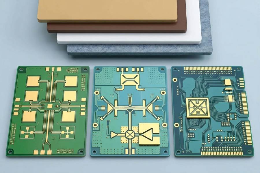
Material Selection for Automotive Radar PCBs
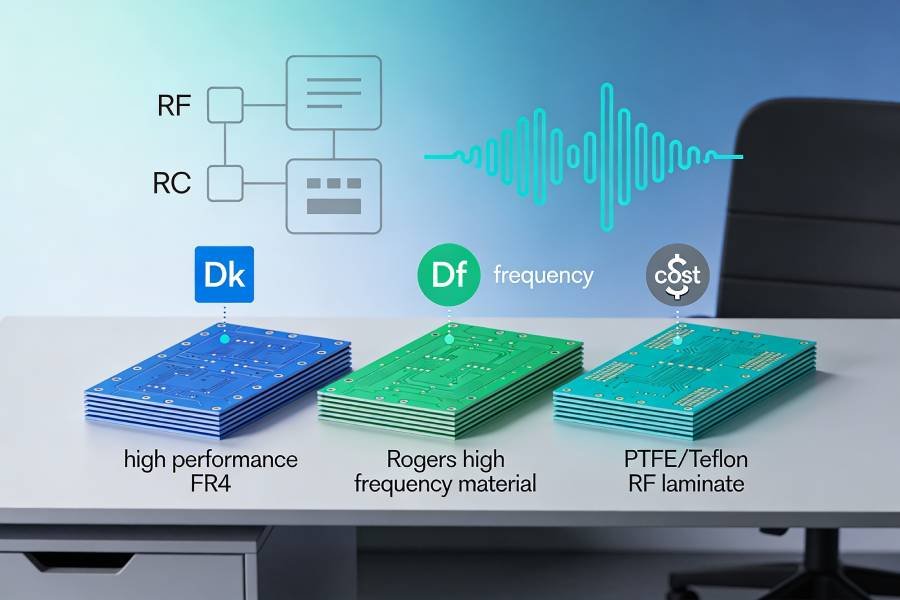
At 77–79 GHz, the automotive radar PCB material has to combine ultra‑low loss and RF stability with automotive‑grade mechanical and thermal robustness. In practice, this means moving beyond standard FR‑4 to specialized high frequency laminates and often hybrid stackups that pair RF materials with high‑Tg FR‑4 on non‑RF layers.
Rogers RO3003 is one of the most widely used materials for 77 GHz automotive radar PCBs because its ceramic‑filled PTFE formulation offers a tightly controlled dielectric constant around 3.0 and an extremely low dissipation factor of about 0.001 at 10 GHz. It also has very low moisture absorption (around 0.04%) and a small thermal coefficient of Dk, so dielectric behavior remains stable across the wide temperature range and humidity conditions seen in automotive environments. These properties make RO3003 and similar ceramic‑filled PTFE laminates well suited for antenna regions, critical RF feedlines, and beamforming networks in 77 GHz radar sensors.
For mixed‑signal radar modules and broader ADAS PCBs, designers often combine such RF laminates with Rogers RO4350B, RO4003C, or other low‑loss hydrocarbon/ceramic materials, plus high‑Tg FR‑4 for control and power sections. RO4350B, in particular, is attractive for ADAS because it supports lead‑free, automotive‑grade manufacturing processes and offers good thermal stability from –40 °C to +125 °C at a lower cost and with more FR‑4‑like processing than pure PTFE. Advanced ADAS designs may also use alternative ceramic‑filled PTFE or high‑frequency composites (such as NF‑30‑class materials) that are explicitly targeted at automotive radar sensors, with data sheets highlighting low loss, controlled Dk, and suitable CTE for reliable via structures in harsh environments.
When you need to turn these material options into a concrete, buildable stackup, our engineers can help you choose practical laminates and thicknesses for 77 GHz automotive radar PCB designs through our high frequency PCB material and stackup review service.
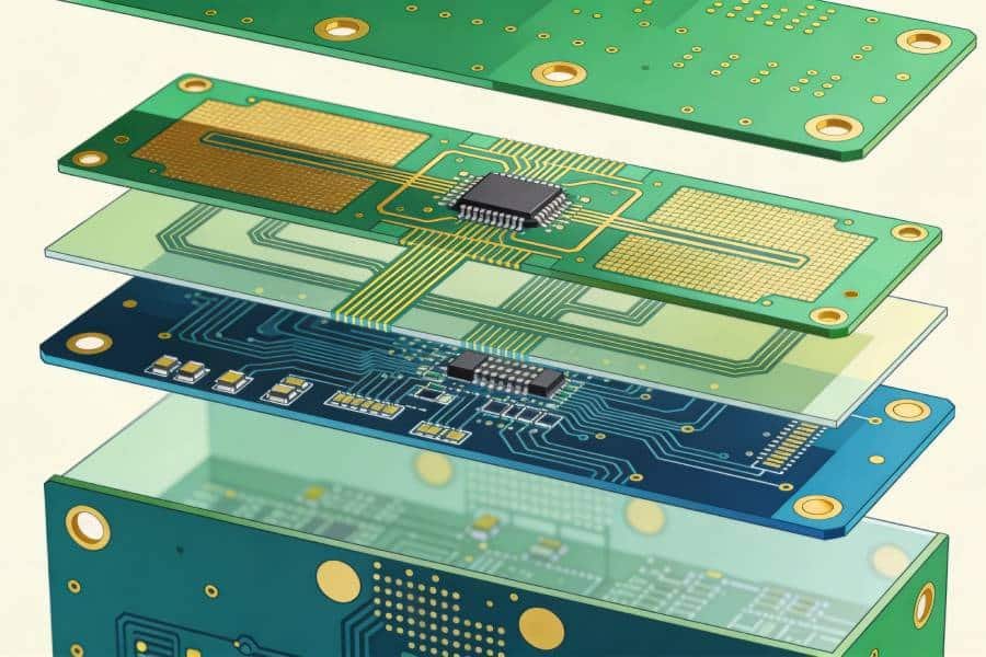
Stackup and Layout Guidelines for Automotive Radar PCB
For most automotive radar PCBs, a simple four‑layer digital stackup is not enough; you typically need at least four to six layers with carefully planned RF and ground planes to control impedance and isolation. A common baseline is a 4‑layer structure with RF components and antennas on the top layer, a solid ground plane directly underneath, a power or mixed‑signal layer on L3, and additional routing or ground on the bottom, while more complex modules move to 6 layers to give separate RF, control, and power routing with multiple reference planes.
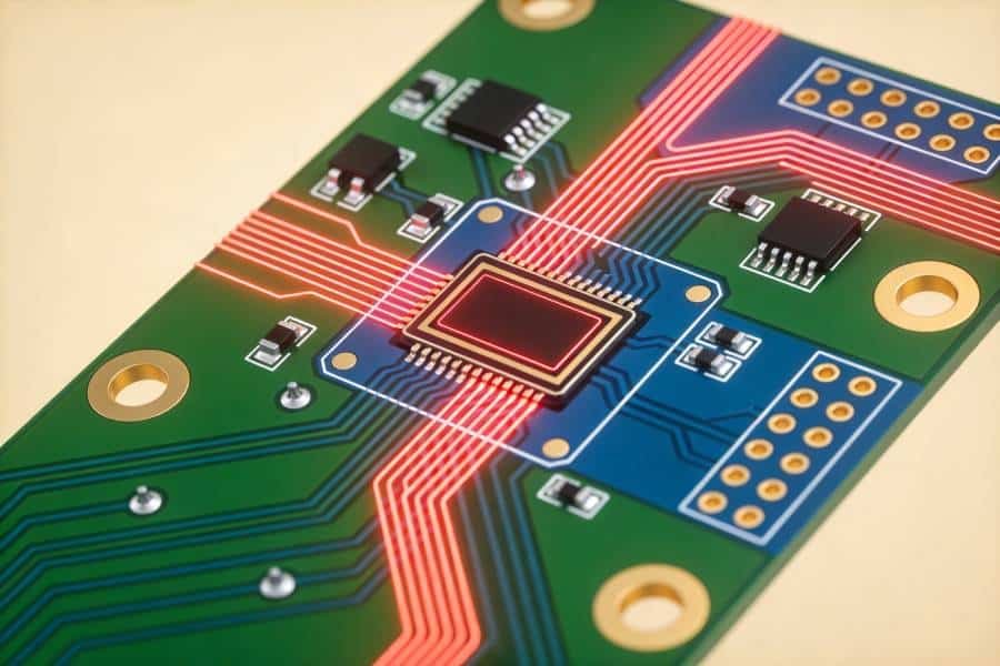
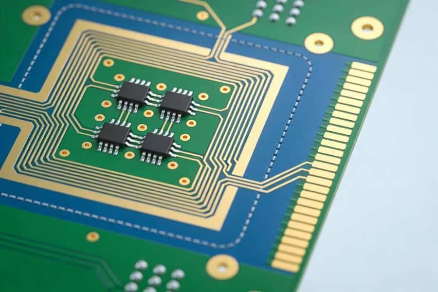
On the RF side, 77 GHz antennas and feedlines almost always live on the outer layer over a continuous ground plane, using microstrip or grounded coplanar waveguide structures with tightly controlled geometry. Antenna regions should be placed at the edge of the PCB or in a dedicated, unobstructed zone that will not be shadowed by tall components, metal housings, or connectors once the module is assembled, and designers often reserve 5–10 mm of keep‑out around the antenna area. Feedlines between the radar transceiver (MMIC) and the antenna array must be as short, straight, and symmetric as possible, avoiding unnecessary bends and via transitions; when bends are unavoidable, use gentle curves or 45‑degree miters rather than sharp 90‑degree corners.
Grounding and isolation are critical because even small couplings at 77 GHz can produce ghost targets or degraded angular resolution. Surround RF traces and antenna regions with dense stitching vias (via fences), typically at 0.5–1.0 mm spacing, tying all ground layers together to suppress surface waves and edge radiation, and keep sensitive RF areas physically separated from noisy digital and switching power circuits. In hybrid RO3003 + FR‑4 designs, maintain a clear mechanical and electrical boundary between the RF laminate region and the FR‑4 control section, and coordinate with your PCB manufacturer on bondply selection and lamination sequence so that the final stackup preserves both RF performance and automotive‑grade reliability.
High Frequency PCB for ADAS: System‑Level Considerations
In real vehicles, the automotive radar PCB never operates alone; it is part of a broader ADAS architecture that also includes cameras, ultrasonic sensors, sometimes LiDAR, and one or more central ECUs or domain controllers. Sensor data typically flows from radar modules over CAN/CAN‑FD, automotive Ethernet, or high‑speed SerDes links into fusion ECUs that run perception and decision algorithms in real time, which means your high frequency PCB for ADAS has to support both mmWave RF and high‑speed digital signaling on the same platform.
From a PCB standpoint, this pushes you toward multilayer or HDI structures that combine low‑loss RF laminates for the 77 GHz front‑end with controlled‑impedance digital layers for gigabit‑class links, all while maintaining clean reference planes and solid isolation between noisy digital and sensitive RF sections. Radar modules connected directly to camera or sensor‑fusion ECUs may also use rigid‑flex or compact connector footprints, so it becomes important to treat the entire signal path—from the radar antenna on the PCB, through connectors or flex tails, into the ADAS ECU—as one continuous RF and high‑speed channel when you plan stackups and routing strategies.
Thermal, Reliability, and Automotive‑Grade Manufacturing
Automotive radar modules pack PAs, LNAs, transceivers, and processing SoCs into small housings, so the automotive radar PCB has to act as a primary heat‑spreading path as well as a high frequency substrate. Effective strategies include placing dense thermal via arrays under hot ICs into internal copper planes or metal baseplates, using thicker copper or dedicated heat‑spreader layers, and designing the module so heat can flow predictably into the vehicle structure or dedicated heat sinks.
Reliability expectations go far beyond consumer electronics, with typical requirements including hundreds of thermal cycles between about –40 °C and +125 °C, combined temperature‑and‑vibration testing, and long‑term operation in high‑humidity conditions without corrosion or delamination. Meeting these targets on an ADAS high frequency PCB means choosing materials with compatible CTEs, robust via and pad geometries, and manufacturing processes that tightly control lamination, drilling, plating, and cleanliness to reduce risks such as solder fatigue and conductive anodic filament (CAF) growth. In practice, automotive radar PCB manufacturing and ADAS PCB platforms rely on automotive‑grade quality systems (such as IATF 16949) and board‑level reliability validation (including temperature cycling, thermal shock, vibration, and THB/85°C‑85%RH tests) to ensure that RF performance and structural integrity stay within spec over the full vehicle lifetime.
Practical Checklist for Automotive Radar PCB and ADAS High Frequency PCBs
To make the ideas in this article usable on real projects, it helps to walk each new design through a short, repeatable checklist. The goal is to align RF performance, automotive‑grade reliability, and manufacturability before you commit to a final stackup and layout.
1. Define the radar and ADAS use case
- What radar type is this: long‑range front radar, mid‑range side radar, short‑range corner radar, or parking radar?
- Which band and modulation are you targeting (for example 76–77 GHz LRR vs 77–81 GHz SRR/FMCW)?
- How does this module connect into the wider ADAS system (standalone ECU, camera fusion ECU, domain controller)?
2. Select appropriate high frequency materials
- For 77–79 GHz RF layers, shortlist low‑loss laminates such as RO3003 or equivalent ceramic‑filled PTFE, and consider RO4350B/RO4003C for mixed RF/digital areas.
- Check Dk/Df, moisture absorption, thermal coefficient of Dk, and CTE compatibility with copper to ensure stable performance over –40 °C to +125 °C and high humidity.
- Confirm your PCB manufacturer can reliably process the chosen materials and has relevant automotive radar PCB experience.
3. Plan an RF‑friendly, automotive‑ready stackup
- Use at least 4–6 layers with RF on outer layers over solid ground planes and separate inner layers for power and control signals.
- If you use a hybrid RO3003 + FR‑4 or RO4350B + FR‑4 stackup, involve your fabricator early to agree on bondply, lamination sequence, and target thicknesses.
- Reserve a clean, unobstructed antenna region with defined keep‑out distances to housings, fasteners, and other PCBs.
4. Apply disciplined RF layout and isolation
- Keep 77 GHz feedlines as short, straight, and symmetric as possible, using controlled‑impedance microstrip or grounded coplanar waveguide.
- Surround RF traces and antennas with tight via fences and solid ground pours, and separate RF from noisy digital and power circuits using distance and shielding.
- Follow radar chipset and antenna reference layouts closely, especially for matching networks, ground patterns, and via placement.
5. Address thermal paths and board‑level reliability
- Identify the hottest devices and design direct thermal paths (pad‑under via arrays to copper planes or metal baseplates) into the module and vehicle structure.
- Choose pad, via, and land patterns that can tolerate repeated thermal cycling and vibration without cracking or solder fatigue, and plan for conformal coating or sealing where needed.
6. Align with automotive‑grade manufacturing and validation
- Work with PCB and PCBA partners that follow automotive quality systems and have documented experience with ADAS radar PCB manufacturing.
- Include board‑level reliability tests (temperature cycling, vibration, THB/85‑85, thermal shock) in your validation plan, and make sure coupon and test‑structure data feed back into your design rules for the next spin.
Conclusion: Turning Automotive Radar Designs into Reliable ADAS Hardware
Automotive radar PCBs sit at a difficult intersection: they must behave like precision 77–79 GHz RF structures, robust automotive electronics, and cost‑efficient mass‑production boards all at once. The right combination of low‑loss laminates, RF‑aware stackups, disciplined layout around antennas and feedlines, and solid thermal and reliability engineering is what turns a promising radar concept into a high frequency PCB for ADAS that works the same on the road as it does in the lab.
In practice, success comes from deciding early how your radar fits into the wider ADAS architecture, selecting materials and stackups your manufacturing partners can actually support, and baking automotive‑grade validation (thermal cycling, vibration, humidity) into the project plan rather than treating them as late hurdles. When automotive radar PCB design, high frequency PCB technology, and automotive‑grade manufacturing are aligned from the start, you can build radar and ADAS platforms that scale across vehicle models and generations with fewer surprises and far less rework.
When your next automotive radar or ADAS design is ready to leave the lab, our end‑to‑end high frequency PCB manufacturing services for automotive radar and ADAS systems can help you bridge the gap from prototype stackups to reliable, automotive‑grade production hardware.