Table of Contents
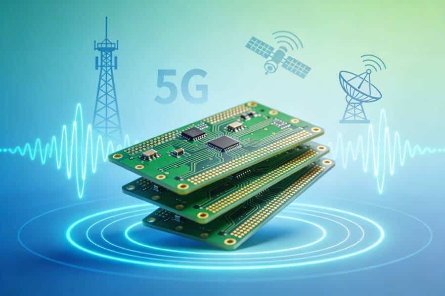
Why PCB Materials Decide 5G, Radar and Satellite Performance
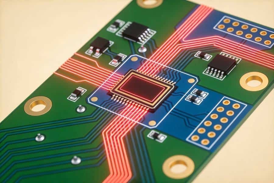
At GHz and mmWave frequencies, the PCB is no longer just a mechanical carrier—it behaves as a critical RF component that sets loss, impedance stability, phase error, and even beam steering accuracy. Choosing the right high frequency PCB material for 5G, the right radar PCB materials, and suitable satellite PCB materials is therefore as important as selecting the active RFICs themselves.
Standard FR‑4 can still work in some lower‑frequency or short‑trace scenarios, but as you move into Sub‑6 GHz 5G, 24–40 GHz FR2 bands, 77 GHz automotive radar, and Ku/Ka‑band satellite links, its loss and dielectric instability quickly become limiting factors. In these regimes, designers turn to engineered high‑frequency laminates—hydrocarbon/ceramic Rogers grades, PTFE and ceramic‑filled PTFE, and increasingly materials like LCP—to control insertion loss, dispersion, and environmental drift while still meeting thermal and reliability requirements. This article explains which material properties matter most at high frequency, then maps specific laminate families to 5G, radar, and satellite applications so you can make grounded, application‑driven choices instead of guessing from datasheets.
If you need a manufacturing partner who can turn these high‑frequency design principles into reliable hardware, our high frequency PCB fabrication services support Rogers, PTFE, and hybrid stackups from quick prototypes to volume production.
Key High Frequency PCB Material Properties You Must Understand
For 5G, radar, and satellite designs, material choice starts with understanding a few core properties rather than memorizing part numbers. The most important are dielectric constant (Dk), loss tangent or dissipation factor (Df), and how both behave over frequency, temperature, and humidity, along with thermal and mechanical characteristics such as CTE and moisture absorption.
Dielectric constant sets impedance, phase velocity, and physical line size. A stable Dk across frequency and temperature keeps impedance and phase consistent, which is critical for phased arrays, long feed networks, and high‑speed backhaul links. Loss tangent (Df) directly limits how long a high‑frequency trace can be before attenuation becomes unacceptable; low‑Df materials are essential for multi‑GHz and mmWave applications, especially when traces are long or cascaded through many components. Beyond Dk and Df, low moisture absorption and good thermal stability help keep those electrical properties from drifting in humid, hot, or space environments—something particularly important for outdoor 5G sites, automotive radar, and satellite payloads that must hold performance over years of operation.
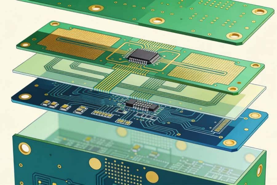
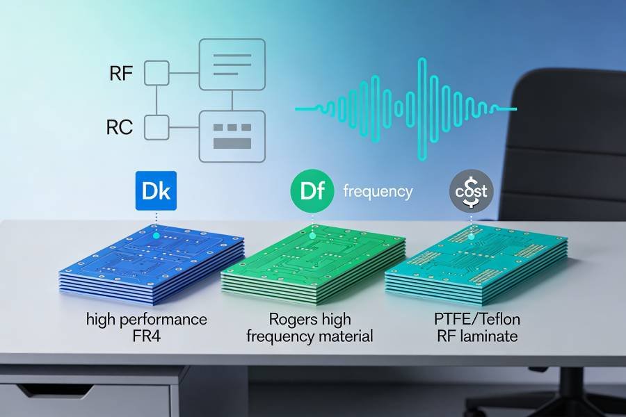
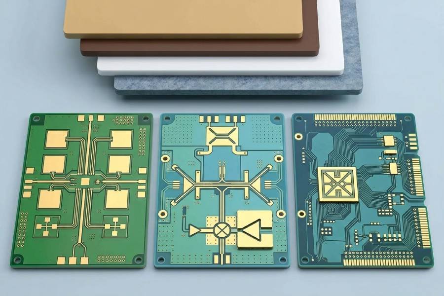
Material Families for High Frequency PCBs: From FR‑4 to PTFE and LCP
High frequency PCB designs for 5G, radar, and satellite rarely use just one “magic” material; instead, they select from a few well‑defined laminate families, each with its own balance of loss, stability, cost, and manufacturability.
High‑performance FR‑4 (baseline material)
High‑Tg, low‑loss FR‑4 is still the default for lower‑frequency RF, short RF traces, and the digital/control portions of mixed RF boards. It offers reasonable Dk (~4.2–4.5), relatively high Df (~0.012–0.02), good mechanical strength, and the lowest cost and broadest fabrication support, which is why it often appears in Sub‑6 GHz 5G designs for non‑critical RF paths and for surrounding digital logic. The downside is higher loss and less stable Dk/Df at multi‑GHz and mmWave frequencies, which is why it is rarely used for long or very high‑frequency RF runs.
Rogers‑class hydrocarbon/ceramic laminates
Rogers RO4000‑series and similar hydrocarbon/ceramic materials are a step up when FR‑4 is marginal for loss and stability but full PTFE seems excessive. They typically provide Dk in the 3.0–3.5 range with much lower Df (around 0.002–0.004) and better Dk stability over frequency and temperature, while remaining largely compatible with FR‑4 processing. This makes them popular for Sub‑6 GHz and lower mmWave 5G, many radar PCB materials in the 24–40 GHz range, and as RF layers in hybrid high frequency PCB material for 5G designs where inner layers remain FR‑4.
PTFE and ceramic‑filled PTFE laminates
Pure and ceramic‑filled PTFE substrates (for example, RT/duroid families) offer the lowest loss and best high‑frequency stability, with Dk values as low as ~2.2 and extremely low Df suitable for mmWave and long RF paths. These materials are the workhorses for demanding radar PCB materials (e.g., 77 GHz automotive radar and high‑power defense radar) and many satellite PCB materials at Ku/Ka/Q‑bands where every tenth of a dB of loss matters. The trade‑offs are higher material cost and more complex processing—special drilling, copper adhesion treatments, and carefully controlled lamination cycles—which require experienced fabricators but deliver unmatched RF performance.
LCP and other advanced RF substrates
Liquid crystal polymer (LCP) and some advanced thermoplastic or composite substrates round out the high‑end options when flexibility, ultra‑low loss, and environmental robustness must coexist. LCP combines low Dk (~2.9–3.2), low Df (~0.002–0.004), very low in‑plane CTE, and inherent flexibility, making it attractive for compact 5G antenna modules, conformal arrays, and certain satellite and radar PCB materials where rigid‑flex or 3D antenna integration is required. Availability and processing are more limited and costly than Rogers‑class hydrocarbon materials, so LCP is usually reserved for space‑constrained or mechanically challenging designs where traditional rigid laminates cannot meet both RF and form‑factor requirements.
High Frequency PCB Materials for 5G Applications
5G hardware spans everything from Sub‑6 GHz RF front‑ends in small cells and CPEs to 24–40 GHz FR2/mmWave modules, and each regime pushes PCB materials differently. The high frequency PCB material for 5G you choose should match not just frequency, but also trace length, power level, form factor, and cost constraints.
For Sub‑6 GHz 5G (around 3–7 GHz), high‑performance FR‑4 can still be workable for short RF runs and non‑critical paths, but many base stations and small cells move critical RF layers to Rogers‑class hydrocarbon/ceramic laminates such as RO4003C or RO4350B to reduce loss and tighten impedance control. A common pattern is to use a hybrid stackup: RF and antenna layers on Rogers with a dedicated ground plane, and inner layers on FR‑4 for digital baseband, control, and power, giving a good balance between RF performance and cost. For longer feed networks, phased‑array panels, or high‑power PAs even at Sub‑6 GHz, Rogers or similar low‑loss materials are strongly preferred as the main RF substrate.
For 24–40 GHz FR2/mmWave 5G, FR‑4 is effectively off the table for RF paths; loss and dielectric variability are simply too high. Here, designers typically choose high frequency PCB materials such as low‑loss Rogers grades (for example RO3003) or PTFE/ceramic‑filled PTFE, sometimes combined with LCP for very compact antenna‑in‑package or module‑in‑package designs. RF feedlines, beamforming networks, and antenna arrays sit entirely on these low‑loss substrates, while digital control and power management may still live on FR‑4 in a hybrid construction beneath or around the RF module. As frequencies climb further (for backhaul links or test equipment above ~40 GHz), PTFE‑based and LCP materials become increasingly dominant because they maintain low Df and stable Dk deep into the mmWave bands.
For real 5G hardware, from Sub‑6 macro base stations to compact FR2/mmWave modules, we can help you move from material selection to a manufacturable stackup through our 5G high frequency PCB manufacturing services.
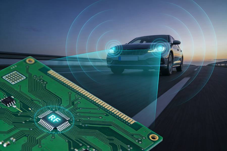
Radar PCB Materials: Automotive, Industrial, and Defense Radar
Radar PCB materials have to support very high frequencies (often 24–81 GHz), high transmit power, and harsh environments, so they sit at the high end of high‑frequency laminates. Compared with typical high frequency PCB material for 5G, radar PCB materials place more emphasis on ultra‑low loss, tight Dk tolerance, thermal stability, and, for automotive and military systems, long‑term reliability over wide temperature ranges.
For automotive radar at 77/79 GHz, popular radar PCB materials include ceramic‑filled PTFE and high‑end hydrocarbon/ceramic laminates such as Rogers RO3003 and RO4350B, often in hybrid stacks with FR‑4 for non‑RF layers. These materials offer very low Df, tightly controlled Dk, and good CTE/thermal behavior, which helps maintain antenna patterns and range resolution as temperature and humidity change, while still fitting into cost‑sensitive automotive manufacturing flows. Many real‑world 77 GHz radar PCBs use constructions like RO3003+FR‑4 or RO4350B+FR‑4 with 4–10 layers, ENIG finish, and mixed lamination plus laser‑drilled blind vias.
Industrial and defense radar PCB materials push even harder on performance and environment. High‑power or long‑range radars often rely on PTFE and ceramic‑filled PTFE composites, sometimes combined with ceramic or metal‑backed substrates, to minimize loss, handle high RF power, and spread heat. In military radar, PTFE‑based laminates with very low Dk (around 2.1–2.5) and Df down to the 0.0004 range are widely used because they preserve signal amplitude and phase over long paths and remain stable across extreme temperatures, moisture, and chemical exposure. For budget‑sensitive or mid‑frequency radar, engineered hydrocarbon/ceramic materials (Rogers, Taconic, etc.) and modified FR‑4 can still play a role, but as frequency and performance demands climb, radar PCB materials trend toward PTFE‑class and ceramic‑enhanced substrates.
If you are working on 77 GHz automotive radar or demanding industrial and defense radar platforms, our radar‑grade high frequency PCB fabrication covers ceramic‑filled PTFE, low‑Dk Rogers, and hybrid constructions with tight process control.
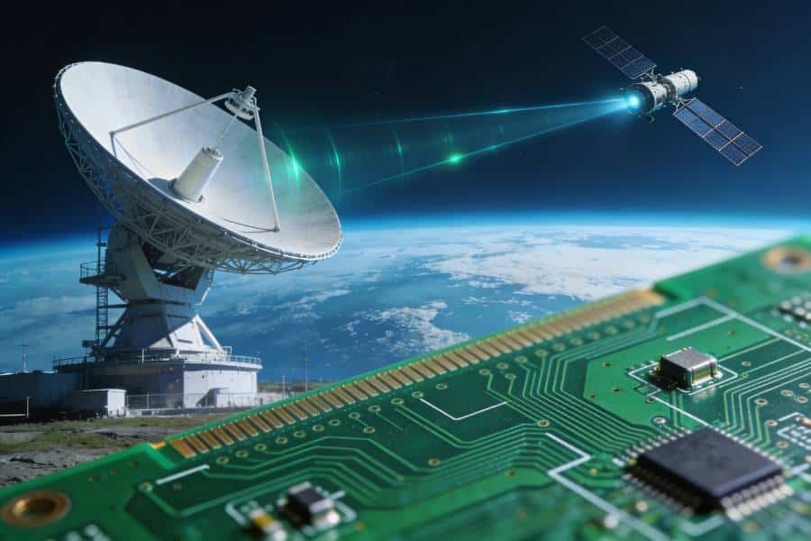
Satellite PCB Materials: L/S‑Band to Ka/Q‑Band
Satellite RF boards move from relatively forgiving L/S‑band links up to extremely demanding Ka/Q‑band front‑ends, so material choices shift from “good RF plus space‑grade robustness” to “ultra‑low loss and phase stability under launch and orbit conditions”.
L/S‑band (1–4 GHz): cost‑aware, radiation‑tolerant
At L/S‑band, designers can often use high‑Tg FR‑4 or space‑qualified polyimide for non‑critical RF plus control and power, while placing critical RF sections on lower‑loss hydrocarbon/ceramic laminates like RO4003C or Taconic RF‑35. These materials give moderate Dk, lower Df than FR‑4, and good thermal and mechanical stability, which is important for withstanding launch vibration, thermal cycling, and some radiation without the cost and processing complexity of pure PTFE.
X/Ku‑band payloads: low‑loss PTFE hybrids
As frequency moves into X/Ku‑band, loss per inch rises and phase stability becomes more critical, so PTFE‑based or ceramic‑filled PTFE laminates start to dominate RF signal paths. A common approach is a multilayer hybrid: PTFE‑based cores (RT/duroid‑class materials) for RF layers and antenna feeds, combined with polyimide or high‑Tg FR‑4 for digital, power, and mechanical support, balancing RF performance with manufacturability and cost.
Ka/Q‑band front‑ends: ultra‑low loss and surface quality
For Ka/Q‑band satellite links (roughly 26–50 GHz), RF PCBs almost always rely on very low‑Df PTFE‑based or advanced materials specifically marketed for Ka/Q‑band SatCom, often with highly controlled Dk and very smooth copper to minimize conductor loss. Materials such as RT/duroid 5880/6002‑class laminates or comparable PTFE composites are widely used for antenna feeds, phased‑array tiles, and waveguide‑to‑PCB transitions, because they maintain low loss and stable phase over wide bandwidths and large temperature swings. At these bands, designers also increasingly consider LCP and flex‑Rogers constructions for compact, conformal, or antenna‑in‑package satellite modules, where flexible low‑loss substrates enable tightly integrated 3D RF layouts.
Practical Selection Framework: Matching Material to Application
A simple way to choose high frequency PCB materials is to first sort by frequency and RF trace length, then refine using environment, manufacturability, and cost.
Step 1 – Start from frequency and RF trace length
- Low frequency / short RF paths
For <5 GHz and very short RF traces (a few centimeters), high‑performance or low‑loss FR‑4 is often sufficient and very cost‑effective. - Mid‑frequency / moderate RF paths
For roughly 5–20 GHz, or Sub‑6 GHz systems with longer feed networks or antenna arrays, move up to hydrocarbon/ceramic materials (for example Rogers RO4000‑class) or similar low‑loss resins, often in hybrid stacks with FR‑4 for inner digital layers. - High frequency / long RF paths
For >20 GHz, 77 GHz radar, and Ka/Q‑band satellite front‑ends, start by assuming PTFE or ceramic‑filled PTFE, and consider LCP only when you also need extreme miniaturization or flex.
Step 2 – Use Dk, Df, and impedance constraints
- Focus on Df (loss tangent)
Above about 5 GHz with appreciable line length, a practical target is Df < 0.005, and in mmWave or long‑range radar/satellite links you often want Df around 0.002 or below. - Choose Dk for both performance and manufacturability
Lower Dk makes it easier to realize 50 Ω with wider traces and looser fabrication tolerances, while higher Dk can shrink antenna and coupler size at the cost of tighter process control and more sensitive simulation. - Check available thicknesses
Because Dk and dielectric thickness together set microstrip/stripline width, always cross‑check your target impedance and stack‑up against the standard core/prepreg thicknesses your fabricator actually stocks.
Step 3 – Overlay environment, thermal, and mechanical demands
- Temperature and thermal cycling
In automotive, industrial, and power‑dense RF sections, prioritize materials with stable Dk/Df over temperature and well‑matched CTE to copper, such as hydrocarbon/ceramic and ceramic‑filled PTFE, and consider metal‑backed or ceramic‑based substrates where heat spreading is critical. - Moisture, outdoor exposure, and aging
For outdoor base stations, radars behind radomes, and marine or humid environments, low water absorption is important; PTFE and high‑end Rogers‑class laminates usually maintain dielectric properties better over time than standard FR‑4. - Vibration, shock, and structural load
In automotive and space, you may combine high‑frequency materials for RF layers with thicker FR‑4 or metal backplanes for mechanical stiffness, ensuring CTE compatibility so solder joints and vias survive long‑term stress.
Step 4 – Check fabrication capability and supply chain reality
- Fabrication difficulty
FR‑4 and most hydrocarbon/ceramic laminates run through standard PCB processes, while pure PTFE, ceramic‑filled PTFE, and LCP demand tighter control of drilling, plating, and lamination; always confirm that your chosen shop has proven experience with the specific family. - Stocked materials and lead time
Many high‑frequency laminates are only stocked in limited thicknesses, copper weights, and panel sizes, so favor materials and thicknesses your fabricator keeps on the shelf to avoid long lead times and higher cost. - Prototype vs. volume production
You can be aggressive with exotic laminates in early prototypes, but for mass production you often end up with a hybrid stack‑up (high‑frequency material for critical RF layers plus FR‑4 for the rest) that balances yield, rework, and total cost of ownership.
Step 5 – Map common applications to material “tiers”
| Application scenario | Typical band / traits | Recommended material tier (by priority) |
|---|---|---|
| General RF, Wi‑Fi, Bluetooth | <6 GHz, short RF traces | High‑performance FR‑4 → low‑loss FR‑4 → entry‑level hydrocarbon/ceramic |
| Sub‑6 5G, small cells, CPE | 3–7 GHz, arrays / medium RF length | Hydrocarbon/ceramic (Rogers‑class) → FR‑4 + RF hybrid stack‑ups |
| 24–40 GHz 5G FR2/mmWave | mmWave, antenna‑in‑package/modules | PTFE / ceramic‑filled PTFE → low‑Dk hydrocarbon/ceramic → LCP for compact/flex |
| 77 GHz automotive radar | EHF, high temp, vibration, cost pressure | Ceramic‑filled PTFE / low‑Dk PTFE → hydrocarbon/ceramic + FR‑4 hybrids |
| Industrial / defense radar | High power, harsh environment | Ceramic‑filled PTFE and PTFE + metal/ceramic backing → high‑end hydrocarbon/ceramic |
| L/S‑band satellite RF | 1–4 GHz, long life, space environment | Hydrocarbon/ceramic + polyimide/FR‑4 hybrids → localized PTFE where needed |
| Ka/Q‑band satellite front‑end | 26–50 GHz, ultra‑low loss, phase‑tight | Ultra‑low Df PTFE / ceramic‑filled PTFE → localized LCP/flex for compact arrays |
Conclusion
High frequency PCB design is ultimately about managing trade‑offs between electrical performance, manufacturability, reliability, and cost rather than chasing a single “best” material. FR‑4, Rogers‑class hydrocarbon/ceramic laminates, PTFE‑based substrates, and LCP each occupy a clear niche on this spectrum, from cost‑efficient low‑GHz workhorses to ultra‑low‑loss, mmWave‑ready platforms for radar and satellite payloads.
Across all of these families, the same core parameters keep appearing: Dk and Df set signal speed, loss, and impedance; copper profile and thickness shape conductor loss; and thermal/mechanical properties like CTE, Tg, and moisture absorption determine whether a stack‑up survives assembly and the field environment. Practical selection therefore starts with operating band and RF path length, then iterates with environmental constraints and the real capabilities of your PCB fabricator, often landing on a hybrid stack‑up that uses premium material only where the RF truly needs it.
For engineers and procurement teams, the key is to treat material choice as an early design decision tied to 5G, radar, or satellite system requirements—not as a late “swap FR‑4 for Rogers” fix—because the right laminate unlocks cleaner layouts, simpler impedance control, and more margin on link budgets. If you share a brief design summary (frequency band, board size, approximate RF path length), I can condense this article into a one‑page material short‑list tailored to that use case.
When you are ready to move from material theory to real boards, you can rely on our end‑to‑end high frequency PCB manufacturing and assembly services to bridge the gap from design, to stackup, to RF‑proven production.