


Table of Contents
Introduction
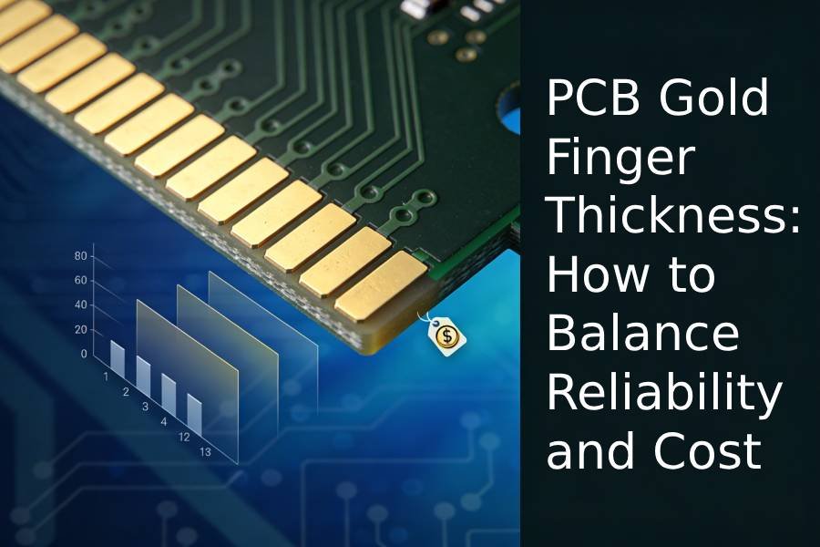
When you design a gold finger PCB, choosing the right plating thickness on the edge connector is one of the most important decisions you make. If the gold layer is too thin, the fingers may wear out quickly, leading to increased contact resistance, intermittent failures and unhappy customers. If you simply ask for the thickest possible gold on every project, your PCB cost can jump by 10–20% or more without necessarily improving real‑world reliability.
Finding the right balance between reliability and cost requires understanding what “gold finger thickness” actually means, how different thickness levels relate to mating cycles and environmental conditions, and how PCB manufacturers price hard‑gold and ENIG options. In this article, we will break down the key concepts, look at typical thickness ranges used in industry and provide practical rules of thumb so you can specify a gold finger PCB thickness that makes both your engineers and your purchasing team happy.
What Does “PCB Gold Finger Thickness” Really Mean?
Thickness of the gold layer, not the whole board
When we talk about “gold finger thickness” in PCB specifications, we are referring to the thickness of the gold plating on top of the nickel underlayer at the edge connector—not the overall PCB thickness or copper thickness inside the board. The typical stack at a gold finger is copper pad → nickel barrier → hard gold or immersion gold, and only the outer gold layer is counted when you see values such as 5 µin, 30 µin or 50 µin. This gold thickness is measured in millionths of an inch (micro‑inch, µin) or sometimes converted to micrometres (µm), where 40 µin is roughly 1 µm.
The nickel underlayer beneath the gold is usually much thicker than the gold itself and serves as a diffusion barrier as well as mechanical support for the contact surface. It prevents the underlying copper from migrating into the gold and maintains the hardness and wear resistance of the contact over time. Because the nickel thickness is generally fixed within a standard range defined by the fabrication process and IPC guidelines, designers rarely specify it directly; instead, they focus on the gold thickness that makes the most difference to both wear life and material cost.
Hard gold vs ENIG: different processes, different thickness expectations
PCB gold fingers are typically finished using either hard electroplated gold or ENIG (electroless nickel immersion gold), and these two processes lead to very different thickness expectations. Hard gold is applied electrolytically on selected areas (usually only the fingers) over nickel, and it can be built up to relatively high thickness levels—10–50 µin or more—making it suitable for high mating‑cycle connectors. ENIG uses a chemical immersion process that deposits a much thinner layer of gold, typically around 1–3 µin, over a phosphorous‑containing nickel layer and is often used as a whole‑board finish rather than just on the fingers.
Because ENIG gold is so much thinner than hard gold, it is excellent for solderability and occasional contact but not ideal for frequent mechanical wiping against connector springs. Designers sometimes assume that “gold is gold,” but from a thickness and wear standpoint, an ENIG‑coated edge connector behaves very differently from one with 30–50 µin of hard gold plating. Understanding which process your fabricator will use on the fingers—and how their standard thickness ranges compare—is essential before you can meaningfully discuss cost trade‑offs.
Units and tolerances in real specifications
In real fabrication notes, you will often see gold finger thickness expressed as a range, such as “hard gold 30–50 µin on edge connectors per IPC‑6012” or “ENIG 1–3 µin per IPC‑4556.” These ranges reflect both process variation and different reliability classes: higher‑end or Class 3 designs may demand thicker, more tightly controlled plating than consumer‑grade boards. It is also common for manufacturers to price discrete “steps” of thickness—such as 5 µin, 15 µin, 30 µin—rather than treating it as a perfectly continuous variable, because each step may require different plating time, bath control and inspection.
From a DFM perspective, the key is to specify a thickness range that meets your mating‑cycle and environmental needs without being more stringent than necessary. If you simply write “heavy hard gold” or “max gold thickness” without numbers, the board house either has to assume a conservative value that pushes up cost, or they must come back to you with questions, delaying the quote. Clear, realistic thickness ranges make it easier for fabricators to pick the right process window and give you an accurate price for your gold finger PCB.
Industry Standards and Typical Thickness Ranges
IPC classes and gold finger requirements
International standards such as IPC‑6012 and related surface‑finish specifications provide general guidance on minimum plating thicknesses for different reliability classes. Class 1 and Class 2 boards, which cover most consumer and general industrial applications, typically allow thinner finishes than Class 3, which targets high‑reliability products such as medical, aerospace or mission‑critical systems. For gold fingers, these standards and common industry practice converge toward a few well‑established thickness bands that balance wear life and manufacturability.
In practice, many PCB manufacturers treat these standards as a baseline and then define their own internal “standard,” “medium” and “heavy” gold options for edge connectors. For example, a fabricator might offer a standard hard‑gold finish around 10–15 µin for general‑purpose designs, a medium option around 20–30 µin for more demanding connectors and a heavy option around 30–50 µin for high‑cycle or Class 3‑style applications. Knowing how your chosen board house maps IPC requirements onto their own process windows is important when interpreting their capability tables and quotations.
Typical thickness bands used in real projects
Looking across manufacturer datasheets and application notes, you will see a few thickness ranges appear repeatedly in gold finger PCB designs.
- ENIG on gold fingers: around 1–3 µin of immersion gold over nickel.
- This is usually the same finish used on the rest of the board and is suitable for prototypes or connectors that see very few mating cycles.
- Thin hard gold: roughly 3–10 µin.
- Often used when some mechanical wiping is expected but the connector will not be plugged and unplugged frequently, or when cost is tightly constrained.
- Medium hard gold: roughly 10–30 µin.
- A common choice for many industrial, communications and computing applications where the connector will see regular but not extreme use.
- Heavy hard gold: roughly 30–50 µin or slightly above.
- Reserved for high mating‑cycle environments, harsh conditions or situations where the cost of failure is very high.
These bands are not rigid rules, but they give a realistic view of what fabricators are used to producing and what purchasing teams often see on quotes. Most projects will fall naturally into one of these categories when you consider the expected lifetime, environment and acceptable cost level.
Matching thickness to reliability class and use case
A convenient way to think about gold finger thickness is to map each band to a rough reliability level and use case. For low‑end consumer products with a short service life and rare connector usage, ENIG or thin hard gold in the 3–10 µin range may be perfectly adequate and helps keep unit price low. For mainstream industrial and networking equipment that must work reliably for years with occasional maintenance or module swaps, 10–30 µin of hard gold is a common and proven choice. For high‑end or critical systems with frequent reconfiguration or harsh environments, specifying 30–50 µin and treating the board as effectively Class 3 in the connector region is often justified.
Of course, these are guidelines rather than strict mandates, and real‑world designs may mix requirements—for example, a largely Class 2 system with a Class 3‑style connector interface. The important point is that once you know which band your application belongs to, you can discuss a concrete target range with your fabrication partner instead of leaving the thickness undefined. This not only leads to more predictable reliability but also makes it much easier to compare quotes and understand how different vendors price their gold finger PCB options.
How Thickness Affects Reliability and Mating Cycles
Wear life and contact resistance
The primary reason to increase gold finger thickness is to extend wear life and keep contact resistance stable over many insertion and removal cycles. Each time the connector is mated, the spring contacts wipe across the gold surface, gradually removing a small amount of material and polishing the contact area. A thin gold layer can be worn through relatively quickly, exposing the underlying nickel and eventually the copper, which are more prone to oxidation and can raise the contact resistance to unacceptable levels.
By contrast, a thicker hard‑gold plating provides more material to absorb this wear and keeps the nickel and copper buried for a much longer portion of the product’s life. This is why high‑cycle connectors in demanding applications rarely use ENIG or very thin hard gold—there simply is not enough gold to survive hundreds or thousands of insertion cycles without performance degradation.
Approximate ranges for different mating cycle targets
Although exact numbers depend on the connector design, environment and cleaning practices, industry guidance and connector vendor data allow us to outline rough relationships between gold thickness and mating cycle capability.
- ENIG or ~3–5 µin hard gold: generally suitable for prototypes, lab fixtures and low‑cycle applications where the connector is only mated a handful of times.
- ~10–20 µin hard gold: often used for connectors expected to see tens to a few hundred mating cycles over the life of the product, such as serviceable industrial modules or networking cards.
- ~30–50 µin hard gold: typically chosen for high‑cycle or mission‑critical connectors that may be plugged and unplugged hundreds or even thousands of times, especially in harsh environments.
These ranges are not hard limits, but they illustrate the general trade‑off: every step up in thickness significantly increases the safety margin against wear, at the expense of more gold usage and thus higher cost.
Environmental and mechanical factors
Gold thickness does not act in isolation; environmental and mechanical conditions can shift the effective requirements up or down. In clean, temperature‑controlled office environments with careful handling, a medium‑thickness hard‑gold finish may easily outlast the nominal mating‑cycle rating because there is little contamination or corrosion to accelerate wear. In contrast, connectors exposed to dust, humidity, vibration or frequent hot‑swap operations may need thicker plating than their nominal cycle count alone would suggest, simply to maintain reliable contacts under less‑than‑ideal conditions.
Mechanical design details such as the contact force of the mating connector, the quality of alignment and the smoothness of the bevel also influence how quickly the gold is abraded. A poorly beveled board or misaligned connector can scrape the plating more aggressively, effectively “using up” thickness faster than expected. When you estimate how much gold you need, it is therefore wise to consider not just the raw number of mating cycles, but also how gentle or harsh each cycle is likely to be.
Practical implications for designers
For most projects, the practical goal is not to calculate the exact number of micrometres needed to survive a specific cycle count, but to place the design in the correct thickness band for its use case. If your edge connector will rarely be touched once installed, ENIG or thin hard gold may be adequate and more economical. If it will be used repeatedly during maintenance, upgrades or reconfiguration, stepping up to a medium or heavy hard‑gold finish provides a relatively low‑cost insurance policy against field failures.
Discussing your expected mating cycles, environment and connector type with your PCB fabricator early on allows them to recommend a realistic thickness range rather than defaulting to either the cheapest or the most expensive option. This collaborative approach typically results in a gold finger PCB that meets reliability expectations without overspending on unnecessary gold.
Cost Impact of Different Gold Finger Thickness Levels
Why gold finger thickness drives cost
Gold is one of the most expensive materials used in PCB fabrication, so it is not surprising that the thickness of the gold finger plating has a noticeable impact on price. The more microns or micro‑inches of gold you specify, the longer the board must stay in the plating bath, the tighter the process control needs to be and the more gold is consumed per panel. On top of raw material cost, higher thickness levels also tend to require stricter inspection and bath maintenance, which add to the overall manufacturing overhead.
For many designs, the gold finger area is only a small fraction of the total board surface, but the cost effect can still be significant—especially when you multiply it across production volumes. This is why board houses usually treat gold finger thickness as a separate pricing parameter, rather than bundling it invisibly into a generic “surface finish” line item.
Typical pricing steps for hard gold
Most PCB manufacturers do not quote every possible thickness individually; instead, they define a few standard “steps” that correspond to internally optimized process windows. While the exact numbers vary by supplier and market conditions, a common pattern looks something like this:
- Thin hard gold (~3–10 µin):
- Often only a modest surcharge over ENIG, sometimes treated as an entry‑level hard‑gold option for light‑duty connectors.
- Medium hard gold (~10–30 µin):
- Typically adds a noticeable premium to the board cost compared with thin gold, reflecting more plating time and tighter control.
- Heavy hard gold (~30–50 µin):
- Usually the most expensive option, with a disproportionately higher price jump because of the extra gold usage and process requirements.
Some vendors express these differences as percentage adders relative to a baseline ENIG or thin‑gold price—for example, a medium hard‑gold option might add around 10–15% to the PCB cost, while a heavy option could add 20% or more depending on panel utilization and market gold prices. Others quote them as fixed surcharges per panel or per design when gold fingers are present.
Balancing cost against real reliability needs
From a purchasing perspective, it can be tempting to always push for the thinnest, cheapest gold option, especially when the connector looks small compared with the rest of the bill of materials. From an engineering perspective, the instinct is often the opposite: ask for the thickest gold available to eliminate any chance of wear‑out. The most cost‑effective designs usually land somewhere between these extremes, using a thickness band that realistically matches the mating cycle and risk profile of the product.
For example, if your connector will only be mated a few times during installation and troubleshooting in a controlled environment, the incremental cost of stepping up from ENIG or thin hard gold to heavy hard gold may not be justified. On the other hand, if a field failure at the connector would require expensive service visits or downtime, the added cost of moving from thin to medium or heavy gold is often a small price to pay compared with the potential impact of premature wear.
A practical way to approach this discussion is to treat gold finger thickness as a design parameter that should be reviewed jointly by engineering and purchasing, rather than a unilateral decision by either side. When you can explain that “this connector needs medium hard gold because it is rated for a few hundred mating cycles in an industrial environment,” it becomes much easier for non‑technical stakeholders to see why a certain premium over the cheapest option is reasonable.
Working with your fabricator on cost‑optimized options
Because each fabrication house has its own plating lines, bath chemistry and cost structure, the exact pricing steps and sweet spots for thickness vary from supplier to supplier. Discussing your expected mating cycles, environmental conditions and volume forecasts with your PCB partner allows them to recommend the most economical thickness that still meets your reliability targets.
In some cases, they may propose hybrid strategies—for example, using heavy hard gold only on specific high‑wear connectors while keeping others at medium thickness, or combining hard gold fingers with ENIG or other finishes on the rest of the board to control cost. Taking advantage of these process‑aware suggestions is one of the easiest ways to optimize the cost–performance balance of your gold finger PCBs without compromising on quality where it truly matters.
Application‑Based Recommendations for Gold Finger Thickness
Consumer electronics and low‑cycle products
In many consumer electronics and light‑duty devices, gold finger connectors are only mated a few times during assembly, testing and final installation. Examples include adapter cards that are rarely removed, plug‑in accessories for home equipment or internal expansion boards that are not intended to be hot‑swapped by end users. For these cases, ENIG or thin hard gold in the 3–10 µin range is often sufficient, provided the environment is clean and the connector is not subjected to frequent vibration or contamination.
Designers in this category can typically prioritize cost while still achieving acceptable reliability by specifying ENIG on the entire board or a low‑thickness hard gold finish on the fingers. It is still important to follow good design rules for beveling, keep‑outs and via placement, but there is usually no need to pay for heavy plating levels aimed at high‑cycle industrial connectors.
Industrial control, networking and communications equipment
Industrial control systems, PLC I/O cards, networking switches, routers and telecom modules often sit in racks or cabinets for many years, but they may be removed occasionally for maintenance, upgrades or troubleshooting. These applications usually experience more temperature variation, dust and vibration than consumer products, and the cost of downtime can be higher. As a result, a medium hard‑gold thickness—roughly 10–30 µin on the gold fingers—is a common and sensible choice.
In this range, the plating can tolerate tens to a few hundred mating cycles with a comfortable safety margin, assuming the connector is designed and used correctly. For cost‑sensitive industrial designs that are only serviced rarely, the lower end of this band may be sufficient, while more critical controllers or line‑card interfaces may justify moving toward the upper end. Discussing the expected service practices and environmental conditions with your fabricator can help fine‑tune where in the medium‑thickness band your design should sit.
High‑reliability, high‑cycle and harsh‑environment systems
Some systems place much higher demands on gold finger connectors, either because they are intentionally hot‑swappable, because they operate in harsh environments, or because the consequences of a poor connection are severe. Examples include field‑replaceable modules in telecom base stations, test fixtures that are reconfigured daily, military or aerospace hardware, and medical equipment where connector failure is unacceptable. In these cases, heavy hard gold in the 30–50 µin range is often recommended.
The extra thickness helps maintain a low, stable contact resistance over hundreds or even thousands of insertion and removal cycles, even in the presence of dust, humidity or moderate corrosive exposure. The incremental cost of this heavier plating is usually small compared with the potential cost of field failures, requalification testing or complex service operations. When specifying designs in this category, it is also important to pay close attention to connector selection, contact force, environmental sealing and cleaning practices to fully realize the benefit of the thicker gold.
Mixed‑use systems and hybrid strategies
Real‑world products often combine different types of connectors and modules with varying criticality and expected usage patterns. For example, a complex system might include a main backplane with high‑cycle line cards, low‑cycle configuration modules and one‑time‑install internal adapters. In such cases, it rarely makes sense to apply the same heavy gold specification to every connector just for the sake of consistency.
A more cost‑effective approach is to group connectors by their reliability and usage requirements and assign thickness bands accordingly—for instance, using heavy hard gold on high‑cycle line cards, medium hard gold on serviceable but less critical modules, and ENIG or thin gold on rarely touched internal connectors. Your PCB fabrication partner can often help you implement these hybrid strategies by selectively applying different plating specifications to different boards or even different connector types across a product family. This targeted use of gold plating ensures that you are paying for extra thickness only where it truly adds value.
Practical Selection Workflow and DFM Tips
A simple decision workflow for gold finger thickness
Instead of treating gold finger thickness as a guess or a negotiation point, you can follow a short decision workflow to arrive at a justified specification.
Step 1 – Define expected mating cycles
Start by estimating how many times the connector is likely to be mated and unmated over the life of the product. Distinguish between “once at installation,” “occasional service” and “regular hot‑swap or reconfiguration” rather than trying to guess an exact count.
Step 2 – Assess environment and criticality
Consider where the equipment will run (office, factory floor, outdoor cabinet, vehicle, etc.) and how serious the impact would be if the connector failed. Clean, benign environments with low criticality lean toward thinner gold, while harsh or safety‑critical conditions push you toward thicker bands.
Step 3 – Map your case to a thickness band
Using your answers from Steps 1 and 2, choose an initial band:
- Low cycles + benign environment → ENIG or thin hard gold (~3–10 µin).
- Medium cycles and/or industrial environment → medium hard gold (~10–30 µin).
- High cycles and/or high‑criticality use → heavy hard gold (~30–50 µin).
Step 4 – Check connector and standards
Verify that your chosen band is compatible with the connector manufacturer’s recommendations and any applicable IPC or customer standards for the product class. If there is a conflict, adjust toward the stricter requirement and document the rationale.
Step 5 – Review cost impact with purchasing
Share the selected thickness band with your purchasing or project management team and ask your fabricator for pricing at that level plus one step above and below. This makes the cost versus reliability trade‑off transparent and allows non‑technical stakeholders to participate in the decision.
Step 6 – Confirm details with your fabricator
Finally, discuss the chosen thickness range and usage scenario with your PCB fabrication partner. They can confirm whether your target is realistic for their process, suggest minor adjustments and help you avoid over‑specifying tolerances that add cost without improving reliability.
DFM tips when specifying thickness
To make this workflow effective in real projects, a few DFM practices are especially helpful.
- Write explicit, numeric thickness ranges in your fab notes
Avoid vague terms like “heavy gold”; instead, specify ranges such as “hard gold 15–30 µin on gold fingers” or “hard gold 30–50 µin for high‑cycle connectors.” Clear numbers prevent misunderstandings and reduce back‑and‑forth during quoting. - Distinguish finger plating from overall board finish
State explicitly whether the rest of the board uses ENIG, HASL, OSP or another finish and note that the specified hard‑gold thickness applies only to the gold finger area. This allows the fabricator to optimize cost by limiting heavy gold to where it is actually needed. - Combine thickness choices with good mechanical design
Remember that bevel angle, connector alignment and keep‑out rules are just as important as thickness in determining wear life. Even heavy gold can wear prematurely if the connector scrapes or if debris accumulates on the contact area. - Ask for feedback from CAM/engineering earlyWhen you send your Gerber or ODB++ package, invite the fabricator’s CAM or engineering team to comment specifically on the gold finger region and thickness choice. Many issues—such as unrealistic tolerances, unnecessary over‑plating or conflicts with panelization—are easiest to fix at this stage.
- Document decisions for future designsAfter a product has been in the field for some time, review its performance and capture lessons learned about whether the chosen thickness band was appropriate. Feeding this experience back into your design guidelines makes it easier to choose the right gold finger PCB thickness on subsequent projects.
How JHYPCB Helps You Optimize Gold Finger Thickness and Cost
Engineering guidance on thickness and reliability
Choosing the right gold finger thickness is easier when you can discuss real‑world usage with a team that understands both design and manufacturing constraints. At JHYPCB, our engineers can review your connector type, expected mating cycles, environmental conditions and reliability requirements, then recommend an appropriate thickness band—ENIG, thin hard gold, medium hard gold or heavy hard gold—that fits your application. This helps you avoid both under‑specifying the finish, which may lead to premature wear, and over‑specifying it, which can drive up cost without tangible benefit.
Flexible gold finger PCB fabrication options
Because we work with multiple qualified PCB and PCBA factories in China, we can support a broad range of gold finger PCB configurations and plating options. For projects that need aggressive cost control, we can focus on ENIG or thin hard gold on the fingers while keeping the rest of the board on a standard finish; for high‑cycle or high‑criticality connectors, we can arrange medium or heavy hard‑gold plating and appropriate inspection steps. This flexibility allows you to implement hybrid strategies across a product family, using heavier plating only where it truly adds value.
Integrated DFM review focused on the connector area
As part of our quotation and pre‑production process, we offer a DFM review that pays special attention to the gold finger region. In addition to checking that the specified thickness is realistic for your reliability targets, we examine bevel notes, via clearances, solder mask openings and inner‑layer copper pull‑back to catch issues that could affect wear life or manufacturing yield. You can simply upload your Gerber or ODB++ files together with the connector datasheet and expected mating cycles, and our team will highlight any recommended adjustments before fabrication begins.
Conclusion: Make Gold Work Where It Matters Most
Gold finger plating thickness is one of the main levers you have to balance connector reliability against PCB cost. Too little gold can lead to early wear‑out and rising contact resistance, while specifying the heaviest possible plating on every connector can inflate board prices without improving real‑world performance for low‑cycle applications. By understanding typical thickness ranges, mapping your design to the right band based on mating cycles and environment, and working closely with your fabrication partner, you can make sure the gold on your edge connectors is used where it delivers the most value.
If you are currently designing or reviewing a gold finger PCB and want help choosing the most cost‑effective thickness, you can learn more about our dedicated Gold Finger PCB fabrication & manufacturing service and request a free DFM review for your next project.


