Table of Contents
Intro
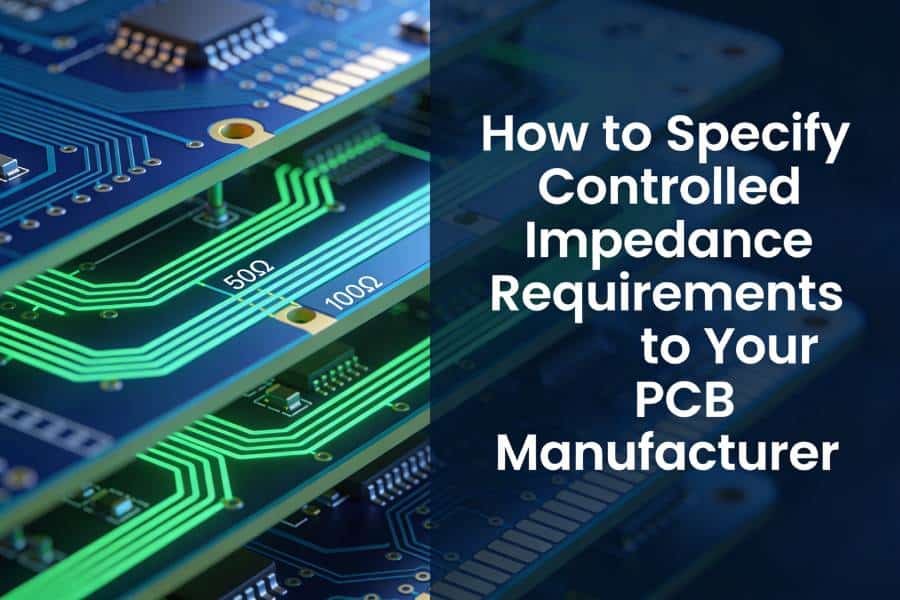
Specifying controlled impedance in your PCB documentation is a critical first step, but it does not guarantee that the finished boards will actually meet those impedance targets. Material tolerances, dielectric thickness variations and small shifts in etching or lamination can all cause the real impedance to drift away from the values you calculated on paper.
For high‑speed serial links, RF paths and other sensitive interfaces, relying on design calculations alone leaves too much risk for late‑stage signal integrity surprises.
To close the loop between design and manufacturing, PCB fabricators use impedance coupons and Time Domain Reflectometry (TDR) measurements to verify how closely production boards match their specified impedance. These tools provide quantitative data on the actual impedance seen by your signals, rather than assumptions based on idealized stackups.
Understanding how coupons and TDR work—and how to request them effectively—helps you interpret impedance reports with confidence and decide when additional testing is worth the cost for your project.
This article explains why verifying controlled impedance matters, what impedance coupons are, how TDR testing is performed in a PCB shop, how to read a typical TDR report and when it makes sense to include coupons and measurements in your fabrication requirements.
If you also want to see how impedance verification fits into a complete manufacturing flow, take a look at our impedance control PCB fabrication services.
Why verifying controlled impedance matters
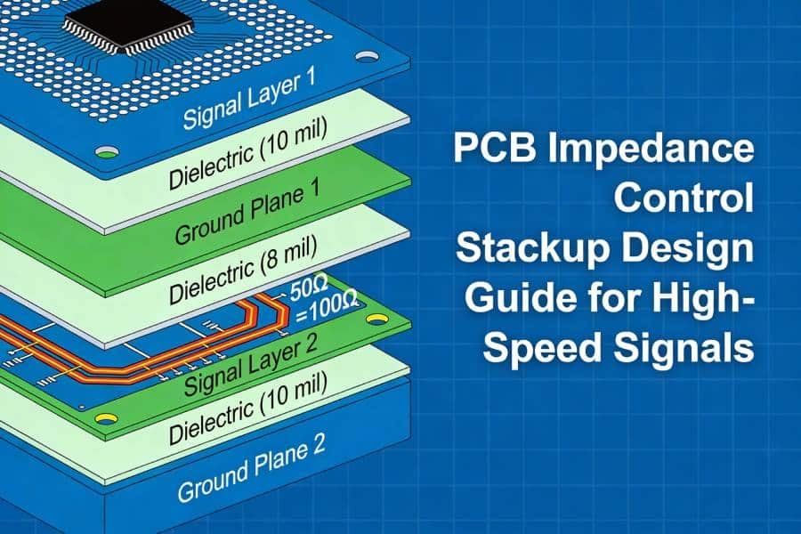
Even when you and your PCB manufacturer agree on a stackup, materials and trace geometries, real‑world processes introduce variability. Resin content, dielectric constant, layer registration and etching conditions can all vary within specified tolerances, and these variations can shift the actual impedance away from its nominal value.
Without measurement, you have no direct visibility into how these process variations affect the impedance of your critical high‑speed routes on a given batch of boards.
For some low‑speed or non‑critical designs, this uncertainty may be acceptable. However, for high‑speed serial links, RF front‑ends, telecom infrastructure and precision measurement equipment, uncontrolled impedance variation can lead to eye‑diagram closure, increased jitter, higher bit‑error rates or degraded noise performance.
In these applications, finding out that the impedance is off only after a system fails a compliance test or behaves unpredictably in the field is both expensive and time‑consuming to fix.
Verifying controlled impedance with coupons and TDR shifts that risk earlier in the process. By measuring representative test structures fabricated on the same panels as your boards, you obtain concrete data about the impedance that your signals will actually see, along with an indication of how consistent it is across a batch.
This information supports more robust qualification, helps you catch process issues before they cause system‑level failures and provides documented evidence of performance for customers and certification bodies.
What is an impedance coupon on a PCB panel?
Purpose of impedance coupons
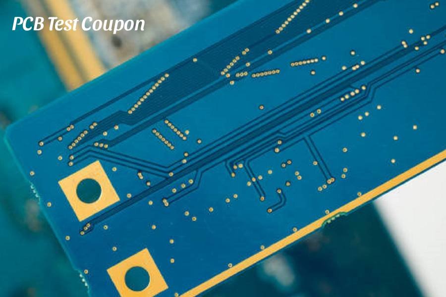
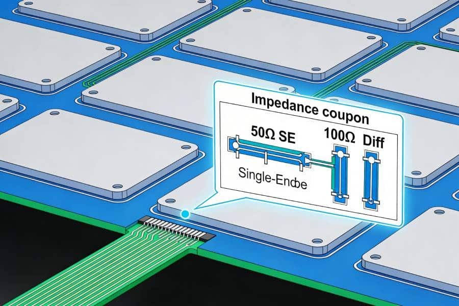
An impedance coupon is a small test structure fabricated on the same production panel as your PCB, designed specifically to represent the controlled‑impedance traces in your design.
Because the coupon shares the same stackup, materials, copper thicknesses and process conditions as the actual boards, its measured impedance provides a realistic snapshot of how the manufacturing process is performing for that batch.
From the manufacturer’s perspective, coupons make it possible to verify impedance without having to probe or damage the finished product boards themselves. They also allow consistent placement of test pads and controlled test geometries, which improves measurement repeatability and simplifies TDR fixturing compared with probing arbitrary traces on the main PCB.
For you as a designer, a well‑designed coupon plus a TDR report offers objective evidence that the boards have been built within the agreed impedance tolerance window, rather than leaving this as an assumption.
Typical coupon structures
A typical impedance coupon includes one or more sections of controlled‑impedance routing that mirror the critical structures in your design. Common examples are 50 Ω single‑ended traces for clock or RF signals and 90 Ω or 100 Ω differential pairs for Ethernet, USB, PCIe or other high‑speed serial interfaces.
These structures are laid out with the same line widths, spacings and layer assignments as the corresponding nets on your board, so that process variations affect them in the same way.
Coupons are usually placed near the edge of the panel, where they are easy to access for probing and can be separated from the main boards after testing.
Clear markings on the coupon identify which structure corresponds to which target impedance and indicate where TDR probes or fixtures should connect, helping ensure that measurements are taken consistently from batch to batch.
Basics of Time Domain Reflectometry (TDR) for PCB impedance
How TDR works in simple terms
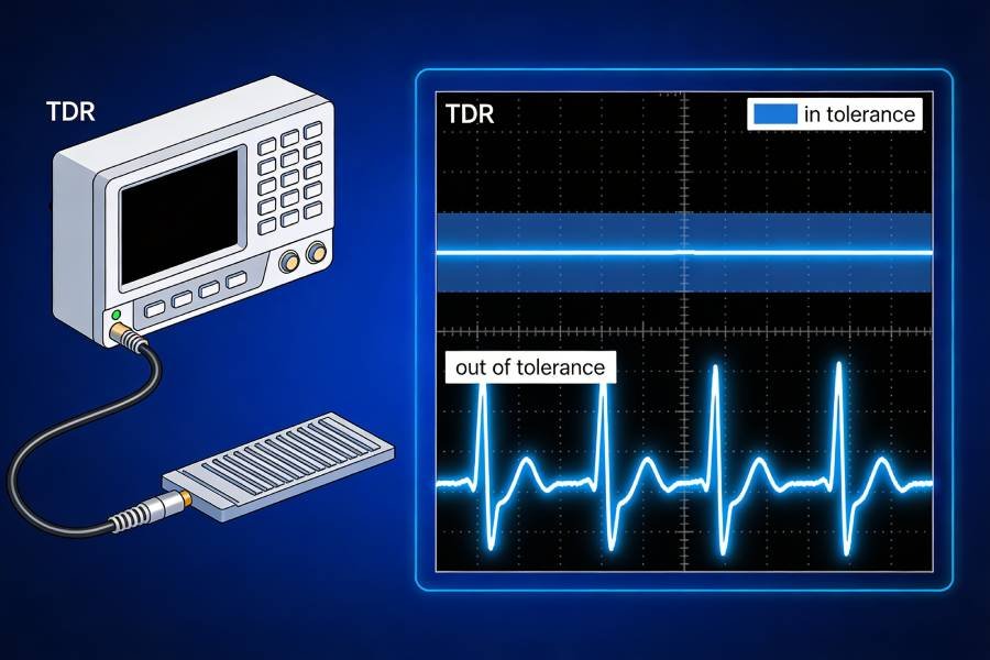
Time Domain Reflectometry is a measurement technique that sends a fast voltage step into a transmission line and observes how much of that signal is reflected back over time.
If the line has a constant characteristic impedance equal to the instrument’s reference impedance, very little energy is reflected and the measured trace appears flat; any change in impedance along the line causes part of the signal to be reflected, which shows up as a deviation in the TDR waveform.
For PCB impedance measurements, the TDR instrument is connected to the coupon through a controlled test fixture and coaxial cable. The instrument launches a fast edge into the coupon and samples the reflected waveform as the step propagates down the test structure.
By converting the time axis into an equivalent distance along the coupon, the TDR trace effectively shows how the impedance varies along the length of the controlled‑impedance segment being tested.
From a designer’s perspective, you do not need to understand every detail of the signal processing inside the TDR. What matters is that the instrument provides a profile of impedance versus distance, along with average values and tolerance information, for the coupon structures that are meant to represent your critical nets.
This turns process variability into measurable data rather than guesswork, and allows both you and the manufacturer to judge whether the impedance control is good enough for your application.
What the TDR trace shows for a good coupon
On a well‑designed and well‑fabricated coupon, the TDR trace for a controlled‑impedance segment will typically show a relatively flat region where the impedance stays close to the target value, with only small fluctuations.
There may be brief deviations at the launch point, connectors or test pads due to unavoidable discontinuities, but the main body of the trace should lie within the agreed tolerance band, such as ±10% around 50 Ω or 100 Ω.
If the trace is consistently higher or lower than the target across the whole coupon, it suggests a systematic offset in factors such as dielectric thickness, material properties or trace geometry.
Localized bumps or dips along the trace can indicate variations in etching, lamination or other process steps that affect impedance in specific regions, which may or may not be acceptable depending on how sensitive your application is to small discontinuities.
By comparing TDR traces and summary statistics across multiple coupons or panels, the manufacturer can monitor process stability over time and detect trends before they turn into field problems.
For you as a customer, reviewing these results—at least for the most critical impedance structures—provides additional confidence that your high‑speed or RF design is being built within the intended electrical constraints.
How PCB manufacturers test coupons during fabrication
Coupon design and panel placement
Before any measurements can be taken, the impedance coupons must be designed and integrated into the production panel layout. PCB manufacturers typically place one or more coupons along the edge of each panel, where they share the same stackup, materials, lamination cycles and etching processes as the product boards.
The routing on these coupons mirrors the controlled‑impedance structures in your design, using the same line widths, spacings and layer assignments, so that any process variation affects the coupons and the actual boards in a comparable way.
Each coupon includes clearly defined test pads or connector footprints that allow a TDR instrument to be connected in a consistent manner. The geometry between the connection point and the controlled‑impedance segment is kept as simple and repeatable as possible to minimize additional discontinuities that could distort the measurement.
By standardizing coupon layouts and their positions on the panel, the manufacturer can streamline both the testing process and the interpretation of results across different jobs and production runs.
TDR test workflow in the shop
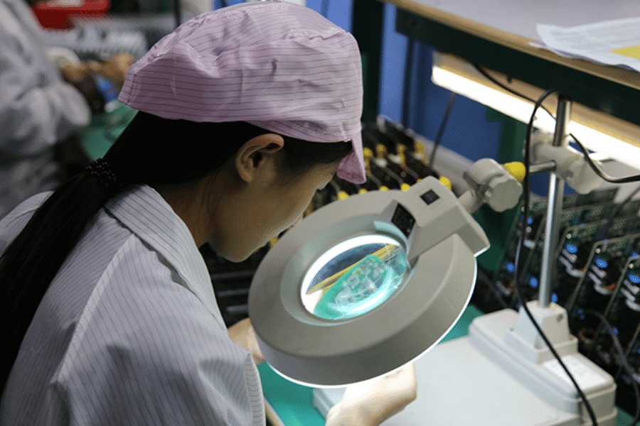
In a typical PCB shop, impedance testing is integrated into the quality control flow for builds that specify controlled impedance and TDR verification. After the panels have passed through lamination, imaging, etching and basic inspections, selected coupons are routed or separated from the panel and brought to the TDR station for measurement.
The operator connects the TDR instrument to the coupon using a calibrated cable and fixture, selects the appropriate test setup and launches the measurement sequence.
The TDR system then records the impedance profile along the length of each controlled‑impedance structure on the coupon and calculates summary statistics such as average impedance, minimum and maximum values and pass/fail status relative to the specified tolerance window.
Depending on your agreement with the manufacturer, this testing may be performed only on first‑article builds, on the first panel of each batch, or more extensively for safety‑critical or highly sensitive products.
When results fall within the expected range, the panels proceed to the remaining fabrication and inspection steps. If the measured impedance is consistently out of tolerance, the manufacturer can pause production, investigate potential causes—such as material deviations or process drift—and take corrective action before releasing boards to you.
In our impedance control PCB fabrication process, coupon design and TDR checks are built into the overall quality workflow for high-speed and RF builds.
This closed‑loop approach helps maintain stable impedance control over time and reduces the risk that out‑of‑spec boards will reach system‑level testing or end customers.
How to read and interpret a PCB impedance report
Key numbers to look at
A typical PCB impedance report summarizes the results of TDR measurements taken on one or more coupon structures, usually corresponding to your main controlled‑impedance targets such as 50 Ω single‑ended and 100 Ω differential pairs.
For each structure, the report often lists the target impedance, the measured average value, the minimum and maximum values observed along the test window and a simple pass/fail indication relative to the specified tolerance.
When reviewing these reports, start by checking that the measured average impedance is reasonably close to the target and that the entire range of values falls within the agreed tolerance band (for example ±10%).
If your design includes multiple controlled‑impedance structures on different layers or with different geometries, make sure each one is represented in the report and that none of the critical nets are missing from the tested set.
Some reports also include TDR plots that show how impedance varies along the coupon as a function of distance. These traces can reveal whether any deviations are localized to specific regions or whether there is a systematic offset across the entire length.
Although you do not need to become an expert in TDR analysis, being able to recognize a generally flat, in‑tolerance trace versus one with large excursions gives you additional confidence when accepting or questioning a batch of boards.
Examples of acceptable vs problematic results
An acceptable result for many applications is a coupon whose measured impedance stays within the specified tolerance window around the target value, with only modest variation along its length. For example, a 100 Ω differential pair that measures between about 92 Ω and 108 Ω, with an average close to 100 Ω, would typically be considered a good outcome for a ±10% specification.
If the trace is slightly biased high or low but still within tolerance and consistent from coupon to coupon, the impact on most high‑speed interfaces will be small, and you may choose to accept the build as is.
More problematic are results where the measured impedance clearly lies outside the specified tolerance, or where there is large variation between different coupons or between different sections of the same coupon. A 50 Ω single‑ended line that consistently measures closer to 60 Ω or 40 Ω, for example, could significantly alter reflection coefficients and might require a discussion with the manufacturer about process adjustments or a potential rebuild.
Likewise, if one coupon passes but another from the same batch fails badly, it may indicate process instability that could show up as performance variation between boards in the field.
When you encounter borderline or out‑of‑spec results, it is important to consider both the severity of the deviation and the sensitivity of your specific application. Some systems with generous margins may tolerate small overshoots, while tightly budgeted high‑speed links or RF paths may not. Involving both your own signal integrity team and the PCB manufacturer’s engineers in this discussion helps you decide whether a given batch of boards is acceptable, needs rework or should be scrapped.
When should you request TDR and coupons?
Not every PCB that includes high‑speed or RF signals requires formal TDR testing and impedance reports. For many lower‑risk designs, agreeing on a well‑defined stackup and letting the manufacturer control their process within normal tolerances is sufficient.
However, there are several situations where requesting coupons and TDR measurements is strongly recommended because the cost of uncertainty is much higher than the cost of testing.
One clear case is when your product must pass rigorous compliance testing or operate with narrow signal integrity margins, such as in telecom infrastructure, base stations, networking switches or high‑end test and measurement equipment.
In these applications, a formal record that impedance has been verified on each batch can support both internal quality assurance and external certification requirements.
It also makes sense to request TDR and coupons when you are introducing a new stackup, using new materials or significantly tightening impedance tolerances compared with previous designs. Early batches are the best time to confirm that the combination of materials, processes and geometries behaves as expected before you commit to large‑scale production.
For safety‑critical or long‑lifecycle products in industrial, medical or aerospace environments, periodic verification on production lots can help you maintain consistent performance over years of manufacturing.
In contrast, for simpler boards with moderate data rates, generous timing margins and low volumes, you may decide that a one‑time verification on first‑article builds is enough, or even that you can rely solely on the manufacturer’s standard process controls. The right level of testing ultimately depends on the risk tolerance, cost sensitivity and reliability expectations of your particular project.
What to include in your TDR and reporting requirements
If you decide that TDR verification is appropriate for your design, it is important to communicate your expectations clearly to the PCB manufacturer. At a minimum, your fabrication notes or purchase order should specify which impedance structures require coupons and TDR measurements, along with their target values and acceptable tolerances.
This helps the manufacturer design appropriate coupons and plan test coverage for the nets that matter most to your system performance.
You should also indicate whether TDR testing is required only on first‑article builds, on the first panel of each production batch or on a more frequent basis. More extensive testing increases confidence but also adds time and cost, so aligning the test strategy with the criticality of each product family is essential.
If your organization has specific quality standards or documentation needs, such as retaining reports for each lot or including them in a product history record, make those expectations explicit up front.
When it comes to the format of the report, focus on the information that will actually help you make decisions. Most engineers find it sufficient to receive the target impedance, measured average, range of values and a clear pass/fail indication for each coupon structure, along with TDR plots when needed.
Requesting highly customized formats or excessive detail can make the process more complex without providing meaningful additional insight, so try to strike a balance between thoroughness and practicality that both you and your PCB manufacturer can support consistently.
Conclusion and next steps
Controlled impedance only delivers its full value when you can trust that the boards leaving the factory match the electrical intent of your design. Impedance coupons and TDR measurements give you a way to turn that trust into measured data, showing how closely real production traces align with your target impedance and how stable the process is over time.
By understanding what coupons are, how TDR works and how to read the resulting reports, you can have more informed conversations with your PCB manufacturer and make better decisions about when additional verification is justified.
For designs where signal integrity, compliance or long‑term reliability are critical, working with a manufacturer that offers robust impedance control, coupon design and TDR testing is especially important.
If you are planning a new high‑speed or RF project and want to define the right level of impedance verification, our team can help you choose suitable coupon structures, test strategies and reporting options as part of our impedance control PCB fabrication service.