Table of Contents
Intro
If you have ever filled out a PCB quote form and hesitated over the “controlled impedance” checkbox, you are not alone. Many designers worry that enabling controlled impedance will increase cost and lead time, but they are also concerned that leaving it unchecked might cause subtle signal integrity problems later in the project.
The reality is that not every PCB needs formal controlled impedance, yet for some designs it is absolutely essential. The challenge is knowing which category your board falls into and how much control is “enough” for your particular combination of signals, interfaces and reliability requirements.
Making this decision thoughtfully can save both money and debugging time by reserving tighter control and additional testing for the designs that truly need it.
This article explains what controlled impedance really means in practice, the technical and commercial factors that determine whether you need it, practical examples of when it is essential and when it is optional, and how to discuss the right level of impedance control with your PCB manufacturer.
If you are already working on a high‑speed or RF design and know that you will need controlled impedance on the finished boards, you can also skip ahead and review our dedicated impedance control PCB fabrication services for a deeper look at available stackups, tolerances and test options.
What “controlled impedance” really means in practice
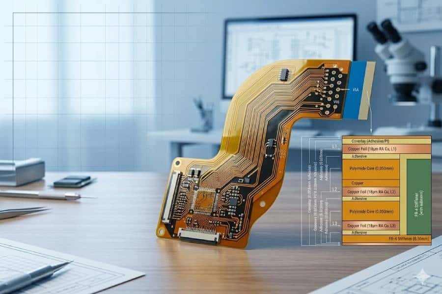
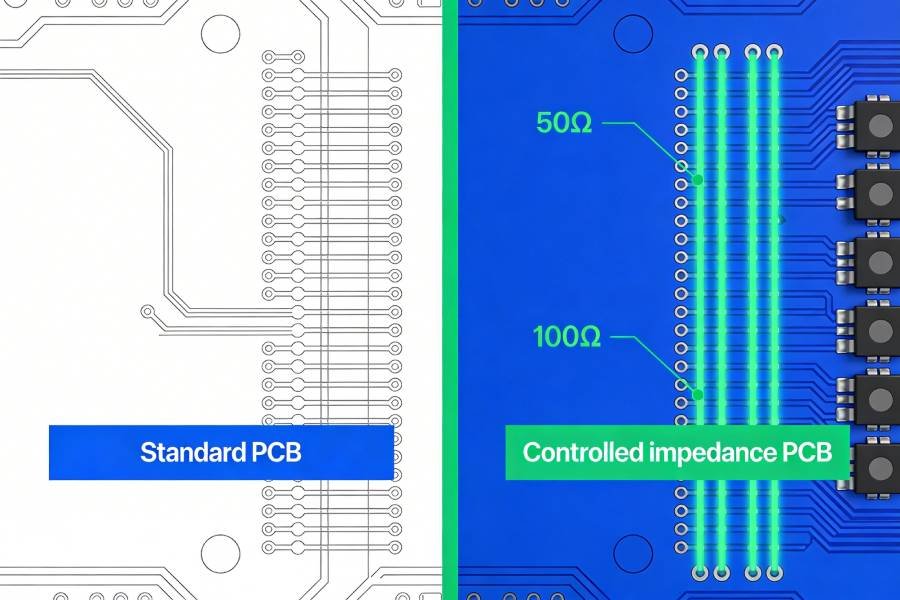
In simple terms, controlled impedance means designing and manufacturing certain PCB traces so that their characteristic impedance stays within a defined tolerance band around a target value, such as 50 Ω single‑ended or 100 Ω differential.
These traces are treated as transmission lines rather than just “wires,” and their geometry, stackup and material properties are chosen so that high‑speed or RF signals see a predictable impedance along their length.
From the manufacturer’s perspective, a request for controlled impedance is not just a note on the drawing; it affects how they select and control materials, define the layer stackup, calculate trace widths and spacings and, in many cases, design impedance coupons and perform TDR measurements to verify the results.
This additional engineering and process control is what allows the finished boards to meet your impedance targets within a specified tolerance window, rather than relying on best‑effort approximations.
Controlled impedance also implies that both you and your PCB supplier have agreed on which nets or signal groups are critical, what their target impedance values and tolerances are and how those requirements are documented in the stackup and fabrication notes.
Without that shared understanding, simply asking for “controlled impedance” provides little real protection against reflections, eye‑diagram problems or inconsistent behavior between different batches of boards.
Factors that determine whether you need controlled impedance
Whether you truly need controlled impedance depends on a mix of signal speed, edge rate, trace length and how tightly your interfaces are specified in terms of impedance and eye‑diagram performance.
As a rule of thumb, once the electrical length of a trace approaches a significant fraction of the signal rise time, it starts to behave like a transmission line and uncontrolled impedance can lead to reflections, ringing and timing uncertainty.
The interfaces used on your board are a major factor: high‑speed serial links such as Ethernet, USB, PCIe, LVDS and many modern memory buses are designed around specific single‑ended or differential impedance values and expect the PCB to match those values within a defined tolerance.
If you follow these standards but do not specify controlled impedance to your fabricator, the actual impedance on the finished board may deviate enough to degrade margin, especially when combined with long runs, tight jitter budgets or marginal connectors.
Board stackup and materials also play a significant role, because dielectric constant, copper thickness and layer‑to‑layer spacing all influence impedance and can vary more widely in uncontrolled processes.
If your design uses dense multilayer stackups, mixed materials (for example, FR‑4 combined with high‑frequency laminates) or very thin dielectrics, you gain a lot by explicitly defining impedance‑critical layers and asking the manufacturer to lock down the stackup and validate it with coupons and TDR measurements.
Typical applications where controlled impedance is essential
In many modern products, controlled impedance is not a “nice to have” but a basic requirement for the PCB to meet interface standards and pass compliance testing.
This is especially true in systems where high‑speed serial links, precise clocks or RF paths are central to the product’s function rather than an isolated feature.
Telecom and networking equipment is a classic example: switches, routers, base stations and optical transport gear all depend on long high‑speed links such as Ethernet, SerDes lanes and backplane connections that assume well‑defined single‑ended and differential impedance throughout the channel.
In these designs, uncontrolled impedance quickly shows up as eye‑diagram closure, bit errors under stress testing and difficulty meeting electromagnetic compatibility (EMC) limits.
Computing, storage and high‑speed digital systems are another large group where controlled impedance is mandatory, because interfaces such as DDR memory buses, PCIe, USB, SATA and high‑speed LVDS links are all specified around characteristic impedance targets.
Motherboards, add‑in cards and high‑density embedded computing boards typically need controlled impedance on many layers, often combined with strict length‑matching and skew constraints.
RF and microwave communication hardware—such as front‑end modules, power amplifiers, antennas and low‑noise receiver chains—relies on controlled impedance transmission lines to connect active devices with filters, matching networks and connectors without creating strong reflections.
Here, even relatively small impedance errors can disturb gain, noise figure and bandwidth, so controlled impedance and appropriate high‑frequency materials are standard practice rather than an exception.
Finally, precision video, imaging and test‑and‑measurement systems often adopt controlled impedance for their high‑bandwidth analog or mixed‑signal paths, including video links, high‑speed ADC/DAC connections and fast sampling front ends.
Instruments and cameras aimed at professional or industrial markets typically require repeatable impedance behavior across builds and over temperature, which is difficult to achieve without formal impedance control and verification at the PCB level.
For projects that fall into these high‑speed or RF categories, it usually makes sense to treat controlled impedance as a baseline requirement rather than an optional upgrade and to work with a manufacturer that can engineer, build and TDR‑verify your key transmission lines.
If you need a starting point, our impedance control PCB fabrication service outlines typical impedance types, stackups and test options that can be tailored to your design.
Situations where you may not need full impedance control
Not every board that carries digital signals automatically requires formal, tightly specified controlled impedance on the fabrication drawing.
For many low‑to‑moderate speed designs, good layout practice and a sensible stackup are enough to achieve reliable performance without adding the cost and complexity of impedance coupons and TDR testing.
If your design is dominated by relatively slow microcontrollers, low‑speed serial buses such as UART, I²C, SPI at modest clock rates, and short on‑board links to simple peripherals, you can usually treat the PCB as a lumped‑element network rather than a set of transmission lines.
In that regime, reflections are heavily damped by the drivers and receivers, and minor variation in trace geometry or dielectric properties has little impact on functionality.
Many industrial control, basic consumer products and simple power‑electronics control boards fall into this category: they may run at tens of megahertz or below, with short trace lengths and generous timing margins.
In these cases it is often more cost‑effective to use standard manufacturing tolerances, follow standard design guidelines for return paths and decoupling and reserve formal controlled impedance for the small subset of products where interfaces are genuinely bandwidth‑limited.
You might also decide that you do not need full impedance control when your high‑speed paths are confined to very short runs inside a module or connector‑to‑chip distance is only a few centimeters and well within the limits recommended by the interface vendor.
Here, using typical stackups, approximate impedance calculators and careful routing can deliver “good enough” impedance behavior without specifying tight tolerance bands or asking the fabricator to validate each controlled structure.
Finally, there are projects where performance requirements are relatively forgiving, such as hobby‑grade equipment, internal test fixtures or early proof‑of‑concept prototypes intended mainly to validate functionality rather than to pass compliance testing.
For those builds, omitting full impedance control can shorten lead time and reduce cost, while you reserve more stringent impedance requirements for later engineering validation or production‑intent revisions.
Cost and process implications of requesting controlled impedance
Requesting controlled impedance is not just a checkbox on the quote form; it changes how your board is engineered, manufactured and inspected, and those changes usually come with additional cost and lead time.
The impact is not dramatic for every project, but you should understand where the extra effort goes so you can reserve it for designs that genuinely benefit from it.
From a process point of view, controlled impedance boards require tighter control of material properties, dielectric thickness and trace geometry than standard builds.
Your manufacturer may need to lock in specific laminates, adjust the stackup, fine‑tune imaging and etching parameters and run impedance simulations to confirm that the target values are achievable before releasing the job to the shop floor.
On top of that, fabricators often add impedance coupons to the production panel and perform TDR measurements, at least on first articles or on a sampling basis for volume orders.
Designing, fabricating and testing these coupons takes time and uses panel area that could otherwise produce saleable boards, which is one of the reasons controlled impedance commands a price premium.
The tighter your requested tolerance, the more pronounced these effects become: asking for ±10% is usually straightforward on common stackups, while demanding much narrower windows may require higher‑grade materials, additional process optimization and stricter in‑process checks.
As tolerances tighten, yield can drop because more panels fall outside the allowed impedance range, and the extra scrap and rework are reflected in the final piece price.
There can also be indirect commercial implications, such as reduced flexibility to substitute materials or move the job between different factories once a specific impedance‑controlled stackup has been qualified for your product.
For that reason, it is wise to align impedance requirements with real system needs rather than applying the same very tight specification to every net, so you can control costs while still protecting the interfaces that truly depend on precise impedance control.
How to decide the right level of impedance control for your project
Choosing the right level of impedance control starts with understanding which signals on your board truly behave as transmission lines and how much performance margin your system has.
If only a few well‑defined high‑speed or RF paths are critical while the rest of the design is relatively slow, you can often limit formal controlled impedance to those specific nets and use standard practices elsewhere.
A practical approach is to classify your signals into tiers: essential high‑speed interfaces that must meet published standards or compliance tests, important but less demanding links where “good engineering practice” is usually sufficient and low‑speed control signals that are largely insensitive to moderate impedance variation.
You then apply the strictest impedance control, tightest tolerances and TDR verification only to the top tier, while relaxing requirements for the others to keep cost and complexity under control.
System‑level considerations also matter, including whether your product must pass formal interoperability or regulatory tests, how long the signal paths are and how easy it would be to debug or redesign the board if issues appear late in the project.
For one‑off internal tools or early prototypes with generous schedules, a lighter touch on impedance control may be acceptable, whereas volume products aimed at demanding markets usually justify more rigorous control and documentation from the very first production‑intent revision.
Finally, your choice should reflect what your manufacturing partner can reliably deliver, based on their materials, stackup options and process controls for impedance‑critical work.
Discussing target impedances, acceptable tolerances and test expectations with your PCB supplier during the quoting and stackup‑definition phase helps you settle on a level of impedance control that aligns with both your technical goals and your budget.
Talking to your PCB manufacturer about impedance needs
A productive conversation with your PCB manufacturer about impedance starts with being clear about which signals really matter and what “success” looks like for your design.
Rather than simply asking for “controlled impedance everywhere,” explain which interfaces are critical, what standards they must meet and whether you need formal test evidence such as TDR reports to support qualification.
It is helpful to come to the discussion with at least a preliminary stackup proposal and a list of target impedances and tolerances, even if you expect the fabricator to refine them.
Sharing information such as signal speeds, expected rise times, connector types and any length‑matching rules you are following gives the engineering team enough context to suggest practical, manufacturable impedance structures.
You should also ask your manufacturer what impedance control capabilities and material options they have, including typical tolerance windows, supported line geometries and whether they recommend standard FR‑4 or higher‑performance laminates for your application.
This two‑way exchange often uncovers simpler stackups or more realistic tolerances that still meet your system needs while improving yield and cost.
Finally, clarify how impedance requirements will be documented and verified before you release the job, including how controlled nets are marked in the fabrication notes, what kind of coupons and TDR sampling plan will be used and how results will be reported back to you.
Agreeing on these details up front reduces the risk of misunderstandings, shortens the quote‑to‑build cycle and gives you greater confidence that the delivered boards will behave as expected in your high‑speed or RF system.
If you prefer to work directly with a team that handles controlled impedance on a daily basis, our engineers can review your Gerber data, proposed stackup and impedance table before fabrication and suggest practical adjustments where needed.
You can share your files and requirements through our impedance control PCB quotation page, and we will come back with a stackup proposal, impedance plan and clear lead‑time and cost information.
Conclusion
Controlled impedance is not something every PCB needs, but it is essential wherever your signals start to behave like transmission lines and must meet defined high‑speed or RF performance targets.
The most cost‑effective strategy is to reserve formal, tightly specified impedance control and TDR validation for genuinely critical interfaces, while using solid standard practices for lower‑speed or less demanding parts of the design.
By classifying nets by criticality, understanding the cost and process impact of tighter tolerances and discussing realistic targets and stackups with your PCB manufacturer early, you can strike a practical balance between signal integrity, manufacturability and budget on your next project.
When you are ready to turn your next high‑speed concept into hardware, you do not have to guess alone.
Send us your design files via our impedance control PCB service page, and we will help you translate your signal integrity targets into a realistic, manufacturable impedance‑controlled stackup.