Table of Contents
Lead-free PCB assembly is now the default in most electronics manufacturing, driven by global environmental regulations and customer expectations for safer products. But while removing lead from solder alloys is good for compliance and sustainability, it also makes the assembly process less forgiving. Lead-free solders typically melt at higher temperatures and have poorer wetting performance than traditional tin‑lead solder, so the process window becomes tighter and defects become more likely if controls are not robust.
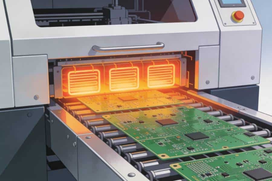
In a lead-free reflow process, peak temperatures often reach the 240–250°C range, which increases thermal stress on components, PCB materials, and solder joints. At the same time, slower and less uniform wetting can contribute to issues such as solder bridging, cold solder joints, voids, and other reliability risks. The result is that what used to be “borderline acceptable” in a tin‑lead process can easily turn into a failure in a lead-free line.
This article looks at the most common defects seen in lead-free PCB assembly and explains why they happen, from process settings and PCB design to material handling and inspection. For each defect, we will walk through what it looks like, the typical root causes, and practical steps you can take to prevent it in production. The goal is to give you a clear, engineer-friendly guide that helps reduce rework, improve long-term reliability, and make your lead-free assembly process more predictable and repeatable.
Why Lead-Free Assembly Is More Challenging
The move from tin‑lead to lead-free solder did not come with a simple “drop‑in” replacement alloy. Lead-free systems, typically based on tin‑silver‑copper (SAC) alloys, have higher melting points and different wetting behavior, which makes the process window narrower and less tolerant of variation. In practice, this means that small deviations in temperature, time, or material condition that might have been harmless in a tin‑lead process can cause visible defects or latent reliability problems in a lead-free line.
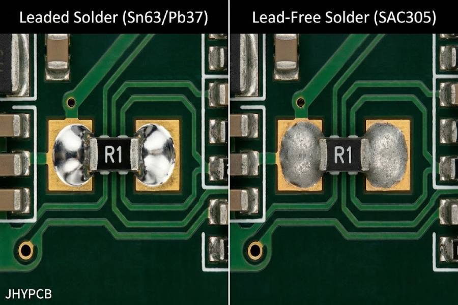
First, lead-free solder requires significantly higher reflow temperatures. While eutectic tin‑lead solder melts at around 183°C, common SAC alloys melt in the 217–219°C range and typically need peak reflow temperatures of 235–250°C to achieve proper wetting. These higher temperatures and longer time above liquidus increase thermal stress on components, PCB materials, and plated through-holes, which can lead to issues like micro‑cracking, delamination, and warpage if the profile is not carefully controlled.
Second, lead-free solder generally wets more slowly and with higher contact angles than tin‑lead solder, often producing duller, less “shiny” joints even when the connection is mechanically sound. This reduced wetting performance makes the process more sensitive to surface oxidation, contamination, flux activity, and board finishes, and it can contribute to defects such as insufficient wetting, de‑wetting, bridging, and voiding when conditions are not optimized.
Finally, because the thermal and wetting margins are smaller, lead-free assembly demands tighter overall process control. Everything from PCB material selection and pad design to solder paste formulation, stencil design, and reflow profile must work together within a narrower tolerance band to consistently produce high‑quality results. When this coordination is missing, the typical outcome is not just one isolated defect, but a higher overall defect rate and more variability in long‑term reliability across the product population.
Common Defects in Lead-Free PCB Assembly
Lead-free reflow and wave soldering tend to produce a familiar set of defects that show up again and again in production lines. Many of these issues also exist in tin‑lead processes, but the higher temperatures and narrower wetting margins of lead-free alloys often make them more frequent and more severe if the process is not tightly controlled. Understanding how each defect looks on the board, what typically causes it, and which parameters you can adjust is the fastest way to reduce scrap, rework, and field failures.
The following sections focus on some of the most common defects in lead-free PCB assembly, including solder bridging, tombstoning, cold solder joints, insufficient wetting, solder balling, voids, head‑in‑pillow, and thermal damage or delamination. For each one, we will connect the visible symptom on the PCB with underlying root causes in design, materials, and process setup, then outline practical steps to prevent the problem from recurring in your line.
Solder Bridging
What it is
Solder bridging is an unintended connection formed when molten solder links two or more adjacent conductive features, such as pads, pins, or fine‑pitch leads. Instead of creating separate, isolated joints, excess solder flows across the gap and solidifies into a bridge that electrically shorts the affected nodes together. Depending on where the bridge forms, this can cause immediate functional failure, intermittent behavior under temperature or vibration, or even permanent damage to components when power is applied.
In surface‑mount assembly, solder bridges are most often seen on fine‑pitch ICs, densely packed connectors, and areas where pad spacing is small relative to the paste volume being printed. In lead‑free processes, the higher viscosity and different flow characteristics of SAC alloys can make bridges more stubborn to eliminate if stencil design, solder mask, and reflow conditions are not well matched to the layout.
Why it happens
At the simplest level, solder bridging occurs when there is too much solder in too little space. Excessive solder paste deposition, whether from an overly thick stencil, oversized apertures, or poor paste release, can create large pools of molten solder that easily flow between adjacent pads. Misalignment during paste printing or component placement can also squeeze solder out of its intended area, pushing it into the gap between leads where it can form a bridge during reflow.
PCB design plays a major role as well. When pad spacing is too tight, pads are oversized, or there is no effective solder mask dam between them, there is little to stop molten solder from wetting across the gap and joining neighboring conductors. This is especially true for fine‑pitch devices, where even small deviations in stencil registration or mask alignment can eliminate the physical barrier that would normally prevent bridging.
Lead-free solder behavior adds another layer of complexity. Because lead-free alloys can be less fluid and wet more slowly than tin‑lead, they may not self‑separate as cleanly once a bridge starts to form. Inadequate or uneven heating can also encourage solder to flow toward warmer leads or pads, increasing the chance that neighboring features are connected by a continuous fillet instead of distinct joints.
Contamination is another common contributor. Residues, dust, moisture, or degraded flux on the PCB surface can disrupt controlled wetting and flow, effectively guiding molten solder along unintended paths between pads. If flux chemistry is not well matched to the lead-free alloy and board finish, or if it is over‑ or under‑activated due to an incorrect profile, the risk of bridging and other wetting‑related defects increases further.
How to prevent it
Preventing solder bridging starts with controlling solder volume. Use a stencil thickness and aperture design appropriate for the pitch and pad size of each component, and consider techniques such as reduced aperture openings or home‑plate shapes for fine‑pitch leads to reduce excess paste between pads. Regularly verify stencil alignment, squeegee pressure, and paste condition to ensure consistent deposition and avoid smearing or scooping that can push paste into narrow gaps.
Good PCB design and solder mask strategy are equally important. Maintain adequate pad‑to‑pad spacing wherever possible, and use solder mask dams between pads to create a physical barrier that blocks molten solder from flowing across the gap during reflow. For critical fine‑pitch devices, review footprint libraries with a DFM mindset and verify that pad sizes, solder mask openings, and land patterns follow current assembly design guidelines.
On the process side, optimize the reflow profile so that pads and leads reach similar temperatures and solder has enough time above liquidus to wet the intended surfaces without slumping excessively. A stable, well‑tuned profile helps minimize uneven flow that can draw solder toward one side and spill into adjacent features, especially in dense areas.
Finally, maintain PCB cleanliness and material control. Store and handle bare boards and components to minimize contamination, and make sure flux type and activity are appropriate for your lead-free alloy and surface finishes. Combined with thorough AOI coverage around fine‑pitch and high‑density areas, these measures significantly reduce solder bridging and the costly rework it creates.
Tombstoning
What it is
Tombstoning, also known as the Manhattan effect or drawbridging, is a defect where a small chip component stands up on one end during reflow instead of lying flat across both pads. In a typical case, one end of an 0402, 0603, or similar passive component remains soldered to its pad while the other end lifts vertically, breaking the connection and creating an open circuit. Because the defect directly interrupts the current path, even a single tombstoned resistor or capacitor can cause a board to fail functional test.
This phenomenon is most common with lightweight surface‑mount passives such as resistors and capacitors, where the component mass is low and the solder surface tension can easily pull one side upward. With ongoing miniaturization and the use of 0201 and 01005 components in lead-free assembly, the risk of tombstoning becomes even more pronounced if design and process conditions are not carefully controlled.
Why it happens
Tombstoning is fundamentally driven by an imbalance of solder wetting forces and timing between the two ends of a chip component. If solder on one pad reaches liquidus earlier, wets more aggressively, or generates a stronger surface tension than the other side, it can pull the component upright as it tries to center itself over the molten solder. The result is a torque that lifts one end off its pad, leaving the component standing like a tombstone.
Several specific factors contribute to this imbalance:
- Pad design and layout issues.
Asymmetric pad sizes, shapes, or copper areas can cause one side to heat and reflow faster, or to develop a stronger solder fillet than the other. Components placed near large copper pours, ground planes, or heat‑sinking structures on one side often see uneven thermal distribution, making tombstoning more likely. - Solder paste printing variations.
Unequal paste volumes on the two pads, misaligned deposits, or printing defects can cause one side to have significantly more molten solder than the other. When one fillet is taller or more voluminous, its surface tension exerts a greater upward force on that end of the component during reflow. - Reflow profile and heating uniformity.
Aggressive ramp rates, poor thermal equilibrium, or non‑uniform heating across the board can cause one pad to reach reflow temperature earlier than the other, especially on mixed‑density layouts. In lead-free processes, the reduced wetting behavior of SAC alloys and the higher peak temperatures can further increase the sensitivity to these timing differences. - Component and surface conditions.
Oxidation on leads, poor solderability, or contamination on one pad can delay wetting on that side, again creating an imbalance. Placement issues—such as skewed components, incorrect Z‑height, or excessive placement force—can also disturb the symmetry of solder contact and encourage one side to lift during reflow.
How to prevent it
Effective tombstoning prevention focuses on restoring symmetry in design, paste deposition, and thermal behavior so that both ends of the component reach and wet in liquidus at nearly the same time.
On the design side, use symmetric pad sizes and shapes that follow the component manufacturer’s land pattern recommendations, and avoid large differences in copper area or thermal mass between the two pads. Place small passives away from major heat‑sinking features when possible, or adjust the layout to balance copper pour and via connections so both ends see similar heating during reflow.
In solder paste printing, aim for equal and well‑controlled paste volumes on each pad. Use appropriate stencil thickness and aperture design for small chip components, and consider slightly reducing aperture size or modifying the aperture shape (for example, trimming paste at the outer edges) to minimize the driving force for tombstoning. Incorporate solder paste inspection (SPI) to verify deposit height and volume symmetry, and correct printing issues before they propagate into reflow.
Reflow profiling plays a critical role as well. A soak‑type profile or a more gradual ramp to reflow can help equalize temperatures across the board and ensure that both solder deposits enter the liquidus phase at roughly the same time. Avoid overly fast heating that exaggerates temperature differences between pads, and confirm that peak temperature and time above liquidus are suitable for your lead-free solder paste and board design.
Finally, maintain good component and PCB surface quality. Use components with reliable solderability, avoid excessive storage times without proper handling, and keep pads clean and free of oxidation or contamination. Verify placement accuracy and pressure settings so that small chips are placed flat and centered between pads, giving the solder equal opportunity to wet both ends instead of pulling the part upright.
Cold Solder Joints
What it is
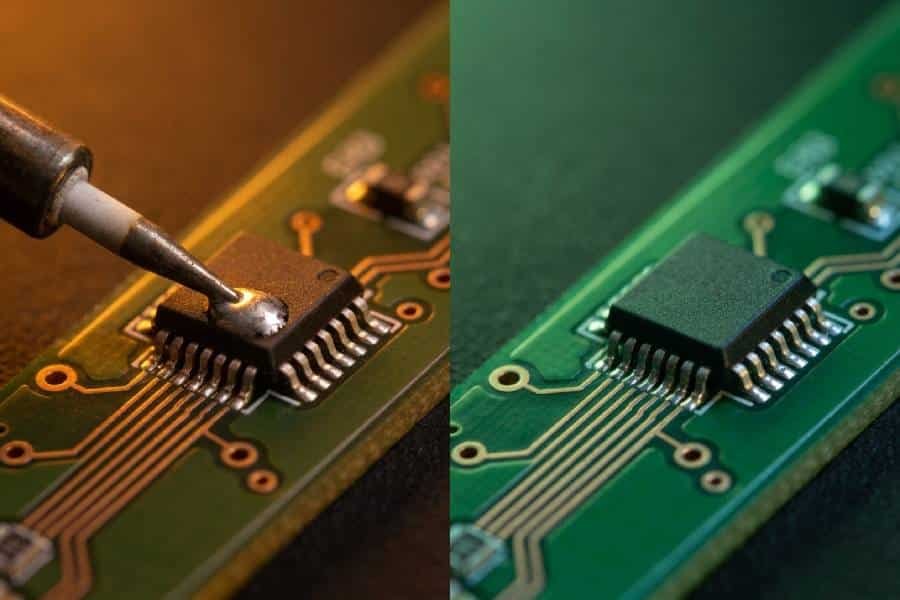
Cold solder joints are improperly formed solder connections where the solder has not fully melted or failed to create a strong metallurgical bond between the component lead and the PCB pad. Visually, they often appear dull, grainy, or rough instead of smooth and uniformly shiny, and the fillet may look irregular, cracked, or slightly convex rather than having a well‑wetted, “volcano‑like” shape. Electrically, cold joints tend to have higher resistance and are prone to intermittent behavior, making them a common root cause of early‑life failures and difficult‑to‑reproduce field issues.
Cold solder joints can occur in both manual and automated processes, and in both SMT and through‑hole assembly. In lead-free PCB assembly, the higher melting point and narrower process window of SAC alloys mean that even small shortfalls in heat, time above liquidus, or surface cleanliness can turn a marginal joint into a cold one.
Why it happens
The primary driver of cold solder joints is insufficient or uneven heat at the solder joint during the reflow or hand‑soldering process. If the pad, lead, and solder do not reach and stay above the alloy’s liquidus temperature long enough, the solder may partially melt, slump, or wet only one surface, freezing before a proper intermetallic bond is formed. In lead-free reflow, this problem is often linked to profiles with peak temperatures that are too low, time above liquidus that is too short, or significant temperature gradients across the PCB.
Several additional factors commonly contribute:
- Poor thermal profile or equipment setup.
Inconsistent oven zones, incorrect conveyor speeds, or poorly tuned profiles can leave some areas of the board underheated, especially on dense or multilayer PCBs. Joints connected to large copper planes or heat‑sinking structures are particularly at risk if the profile is not designed to compensate for their higher thermal mass. - Contamination and oxidation.
Oxides on pads and component leads, as well as residues, dust, or high humidity, interfere with flux action and prevent solder from properly wetting the surfaces. In a lead-free process where wetting is already less robust than tin‑lead, any additional barrier to wetting significantly increases the likelihood of cold joints. - Inadequate or degraded flux.
If flux activity is too low for the board finish or level of oxidation, or if the flux is driven off too early by an aggressive preheat, solder may not wet fully before solidifying. Expired or improperly stored solder paste can also exhibit weakened flux performance, resulting in incomplete bonding. - Manual soldering issues.
In hand‑soldered areas or rework, cold joints often stem from using an iron temperature that is too low, applying heat for too short a time, or failing to heat both the pad and the lead simultaneously. Poor technique—such as moving the joint while it cools or applying solder only to the iron tip instead of the joint—can leave behind a weak, mechanically fragile connection.
How to prevent it
Preventing cold solder joints starts with establishing and maintaining a robust thermal profile for lead-free assembly. Ensure that each joint reaches a peak temperature safely above the alloy’s liquidus (typically at least 15–25°C higher) and that the time above liquidus is long enough to promote full wetting and intermetallic formation without overstressing components. Use thermocouples on representative boards—including joints connected to heavy copper or ground planes—to validate that even the “coolest” locations meet these criteria.
Surface preparation and material quality are equally important. Keep PCB pads and component leads clean and properly stored to minimize oxidation and contamination, and bake moisture‑sensitive boards when required. Select high‑quality lead-free solder paste with suitable flux activity for your finishes, and follow the manufacturer’s guidelines for storage, thawing, and working life to avoid degraded flux performance.
Process controls should also cover paste printing and environmental conditions. Consistent solder paste deposits help ensure that each joint has enough material to form a solid connection once the profile is correct, while stable temperature and humidity in the production area reduce the risk of surface contamination and paste drying. Incorporating AOI to flag suspicious fillets and, where needed, selective X‑ray or cross‑section analysis on critical products can help you catch and eliminate cold joints before boards leave the factory.
For manual soldering and rework, use temperature‑controlled soldering stations set appropriately for lead-free alloys, and train operators to heat both the pad and the lead evenly before applying solder. Encourage the use of additional flux where needed, and emphasize allowing joints to cool naturally without movement so the solder can solidify into a strong, well‑wetted fillet.
Insufficient Wetting
What it is
Insufficient wetting is a soldering defect where the solder melts but does not properly spread and bond to the PCB pad, the component lead, or both. Instead of forming a smooth, continuous fillet with a low contact angle, the solder may sit like a blob, partially wrap around the lead without gripping the pad, or cover only a small portion of the metallized surface. In some cases, the solder initially wets and then pulls back, leaving exposed metal or thin, uneven films—a behavior often referred to as de‑wetting.
Visually, insufficiently wetted joints often look irregular, with edges that do not “feather out” onto the pad, and you may see clear boundaries where solder simply refuses to spread further. Even if such joints appear mechanically stable at first glance, the limited contact area and weak metallurgical bonding can lead to high contact resistance, intermittent connections, and reduced long‑term reliability under thermal or mechanical stress.
Why it happens
Insufficient wetting usually indicates that something is preventing the molten solder and flux from doing their job—either the surfaces are not solderable, the flux is not active enough, or the thermal conditions are not suitable for proper wetting. In lead-free assembly, where solder alloys have higher surface tension and inherently poorer wetting than tin‑lead, any additional barrier can quickly result in visibly poor spread and incomplete fillets.
Common root causes include:
- Surface contamination and oxidation.
Oils, fingerprints, dust, plating residues, or solder mask contamination can physically block solder from contacting the base metal. Oxidized pads or component leads, especially on sensitive finishes or long‑stored materials, make it difficult for flux to remove the oxide layer, so solder beads up instead of flowing out. - Inadequate or mis‑applied flux.
If the flux activity level is too low for the board finish, or if the flux is consumed or burned off too early by an aggressive preheat, it cannot keep surfaces clean during the critical time above liquidus. Expired solder paste or paste that has been improperly stored often shows reduced flux effectiveness, leading directly to non‑wetting and de‑wetting issues. - Incorrect thermal profile or insufficient heating.
Pads, leads, and solder must all reach and remain above the alloy’s liquidus temperature long enough for the flux to activate and for solder to spread. If certain areas of the PCB are cooler—due to heavy copper, poor oven uniformity, or too short a soak or time above liquidus—solder may melt but never fully wet the surfaces before solidifying. In lead-free processes, where the required peak and wetting temperatures are higher than tin‑lead, this margin for error is even smaller. - Material compatibility and plating issues.
Some surface finishes and lead platings are inherently more difficult to solder, especially if plating thickness is low or inconsistent. Mismatch between flux chemistry and the board finish, or degraded finishes due to improper storage, can further reduce solderability and promote non‑wetting or de‑wetting behavior.
How to prevent it
Preventing insufficient wetting requires a combination of clean, solderable surfaces, appropriate flux chemistry, and well‑controlled thermal conditions. Start by ensuring that PCB pads and component leads are stored and handled to minimize contamination and oxidation—use gloves where appropriate, avoid touching solderable areas, and follow recommended shelf‑life and storage conditions for each finish. Inspect incoming materials for solderability when possible, and avoid using boards or components that show obvious discoloration, heavy oxidation, or plating defects.
Select solder pastes and flux systems with sufficient activity for your lead-free alloy and board finishes, especially if you work with more challenging surfaces. Follow the manufacturer’s guidelines for storage, thawing, and stencil life to keep flux performance within specification, and do not use expired or out‑of‑spec paste that can no longer provide reliable wetting.
On the process side, optimize the reflow profile to give solder and flux enough time and temperature to work effectively. Use a soak phase that equalizes temperatures across the PCB, then maintain adequate time above liquidus for the lead-free alloy to fully wet the pads and leads without overheating sensitive components. Verify with thermocouples placed on representative locations—including high‑mass and edge areas—to confirm that the coolest joints still reach the necessary wetting temperature.
Finally, monitor wetting behavior through inspection and feedback. Use AOI to flag joints with abnormal shapes or contact angles and, when necessary, complement it with cross‑section or X‑ray analysis for critical applications. If you see recurring insufficient wetting in specific areas or component types, treat it as a signal to review surface finishes, flux compatibility, and local thermal conditions rather than just reworking the symptoms.
Solder Balling
What it is
Solder balling is a defect where small, spherical beads of solder form and remain on the PCB surface or around solder joints after reflow. These solder balls can appear along solder mask edges, between pads, under components, or scattered across the board, rather than coalescing into the intended joints. While some tiny, isolated balls may be purely cosmetic, excessive solder balling increases the risk of shorts, leakage paths, and reliability problems—especially if balls move or dislodge during handling or in the end application.
In lead-free SMT assembly, solder balling is particularly common around fine‑pitch areas and where paste volumes are high, such as large pads or dense component clusters. The combination of higher reflow temperatures, different flux chemistries, and narrower process windows makes it more important to control paste behavior and thermal gradients to prevent solder from spattering or separating into discrete spheres.
Why it happens
Solder balls typically form when portions of solder paste are separated from the main deposit during heating and then solidify on the board instead of merging back into the joint. This separation can be driven by excessive paste volume, rapid outgassing of volatiles or moisture, poor wetting, or mechanical disturbance of the paste before or during reflow.
Common root causes include:
- Excessive solder paste and stencil issues.
Applying too much paste, using an overly thick stencil, or having oversized or poorly gasketed apertures can leave surplus solder that easily breaks away and forms balls during reflow. Misaligned or dirty stencils allow paste to smear under the stencil or onto solder mask areas, where it is more likely to bead up instead of forming a proper joint. - Moisture and volatile content in paste and PCB.
Solder paste is hygroscopic and can absorb moisture if not stored or handled correctly; PCBs can also retain moisture in the laminate and pads. During preheat and reflow, this trapped moisture rapidly vaporizes and can “spit” solder particles away from the main deposit, which then cool into isolated solder balls. - Incorrect reflow profile and rapid heating.
Profiles with too steep a ramp, inadequate preheat, or excessive peak temperatures can cause violent boiling of solvents and flux, splattering solder droplets onto the board. If flux fails to activate properly during preheat, solder may not coalesce smoothly and can instead separate into small spheres as it melts and solidifies. - Poor surface cleanliness and wetting.
Contaminants such as oils, dust, or residues on the PCB or component leads prevent solder from wetting and flowing into the intended joints, encouraging solder to ball up on solder mask or non‑solderable areas. Insufficient solder mask coverage or misaligned mask openings can also leave exposed areas where solder can spread and then fragment into balls during reflow.
How to prevent it
Reducing solder balling starts with controlling solder paste volume and deposition quality. Use an appropriate stencil thickness for the component mix, optimize aperture sizes and shapes to avoid over‑printing, and ensure good gasketing between stencil and PCB so paste does not leak onto solder mask. Clean stencils regularly to remove dried or smeared paste, and verify printer alignment and squeegee parameters to maintain consistent, well‑defined deposits.
Next, manage moisture and paste handling carefully. Store solder paste under the recommended temperature and humidity conditions, allow it to equilibrate to room temperature before opening, and respect its working life on the stencil. Keep PCBs dry by using proper packaging and, when necessary, baking boards to drive out moisture before assembly, especially for moisture‑sensitive laminates or after long storage.
Optimize the reflow profile to provide a gradual preheat that allows solvents and moisture to evaporate gently, followed by a controlled soak and a peak within the recommended range for your lead-free alloy. Avoid excessively fast ramp rates or unnecessarily high peak temperatures, which can cause spattering and prevent solder from coalescing into smooth joints.
Finally, ensure good surface cleanliness and solder mask design. Keep PCB surfaces and component leads free of contamination by following clean handling practices, and verify that solder mask openings and coverage are correct so solder is confined to the intended pad areas. For high‑reliability or particularly sensitive applications, consider using a nitrogen atmosphere in reflow to reduce oxidation and promote better wetting and coalescence, which can further reduce solder balling.
Voids
What it is
Voids are internal cavities or gas pockets trapped inside a solidified solder joint, typically visible as dark, round or irregular areas when inspected by X‑ray. Unlike surface defects, voids are hidden within the bulk of the solder, so the joint may look normal externally while containing a significant amount of empty space inside. Excessive voiding reduces the effective cross‑section of solder that carries current and heat, creating localized stress concentrations that can accelerate crack initiation and growth under thermal cycling or vibration.
Voids are especially critical in BGA, QFN, and other bottom‑terminated components, as well as in large thermal pads and power devices where solder joints double as thermal paths. In these applications, high void content can degrade thermal conductivity, increase junction temperatures, and compromise both electrical performance and long‑term reliability.
Why it happens
Voids form when gases generated during the soldering process cannot escape from the molten solder before it solidifies. These gases can come from flux volatiles, solvents, moisture, or contamination on the PCB and component surfaces, and they tend to become trapped under large pads or within area‑array joints where escape paths are limited.
Several main factors drive voiding:
- Solder paste outgassing and flux chemistry.
As solder paste heats up, the flux activates and releases gases; if the heating rate is too fast or the flux contains many volatile components, large bubbles can form and become trapped in the molten solder. Some lead-free pastes and specific alloy/flux combinations are more prone to macrovoiding than others, especially under large pads or in BGA balls. - Reflow profile and thermal behavior.
Profiles with short or inadequate soak times, overly steep ramps, or suboptimal peak and time‑above‑liquidus conditions may not give gases enough time to escape before the solder freezes. Uneven heating across the board can further trap flux volatiles in cooler regions, leading to higher void percentages in certain joints. - Stencil and pad design.
Large, uninterrupted paste deposits under thermal pads or BGAs can trap gases with no easy escape route. Stencil designs that do not segment these areas—such as solid apertures instead of window‑pane or cross‑hatch patterns—tend to produce more voiding. Pad finishes and plating impurities can also influence void formation by affecting wetting behavior and interfacial reactions. - Board and component contamination or moisture.
Moisture absorbed into the PCB or components, as well as organic residues or plating impurities, can vaporize during reflow and create additional gas sources within the joint. If these gases are released late in the reflow cycle or under large, low‑clearance components, they are more likely to be trapped and form voids.
How to prevent it
Reducing voids requires controlling gas generation and providing escape paths before the solder solidifies. A good starting point is to choose low‑voiding solder pastes and flux chemistries designed for lead-free BGA, QFN, and thermal‑pad applications. Work closely with your paste supplier to select formulations with optimized volatile content and wetting behavior for your board finishes and package types.
Next, optimize the reflow profile with void reduction in mind. Use a controlled preheat and soak stage to allow flux volatiles and moisture to outgas gradually, rather than boiling violently near peak temperature. Ensure adequate time above liquidus so that bubbles can rise and escape from the molten solder, while keeping peak temperature within the recommended range for your lead-free alloy and components. For demanding applications, consider vacuum‑assisted reflow, which can dramatically lower void content by actively pulling gases out of the joints while the solder is molten.
Stencil and pad design are also powerful levers. For large thermal pads and bottom‑terminated components, segment the paste pattern using window‑pane, cross‑hatch, or similar aperture designs that break up the deposit and create channels for gas escape. Avoid over‑printing paste under these components, and follow proven design guidelines for BGA ball pads and thermal land geometry to balance solder volume and venting paths.
Finally, control cleanliness and moisture. Store PCBs and components according to their MSL and finish requirements, and bake them when necessary to remove absorbed moisture before assembly. Maintain a clean process environment to minimize contaminants that can decompose or outgas during reflow, and use X‑ray inspection to monitor void levels in critical joints so profile and material adjustments can be made proactively rather than after failures occur.
Head-in-Pillow
What it is
Head‑in‑pillow (HiP), also called head‑on‑pillow or ball‑in‑socket, is a soldering defect that occurs mainly with BGA, CSP, PoP, and other area‑array packages when the solder ball and the solder paste both reflow but fail to fully coalesce into a single joint. In cross‑section or 3D X‑ray, the joint looks like a spherical “head” resting on a flattened “pillow” of solder paste, with a visible interface or gap between the two instead of a continuous metallurgical bond. Electrically, HiP joints may be open or highly intermittent, and because the defect is hidden under the package, it often escapes visual inspection and can cause hard‑to‑diagnose field failures.
HiP has become more prevalent in lead-free assembly, especially with SAC‑based BGA balls and fine‑pitch packages that are sensitive to warpage and wetting conditions. The defect tends to appear at the outer rows or corners of BGAs where package warpage is greatest, and it is frequently misinterpreted as simple voiding if only low‑resolution 2D X‑ray is used.
Why it happens
Head‑in‑pillow is essentially a non‑wetting defect driven by a combination of poor wetting and dynamic warpage of the PCB and package during the reflow process. During heating, the PCB and BGA substrate expand and can flex or bow, causing some solder balls to lift away from the molten paste on the pads and break contact while both are in a liquid or semi‑liquid state. Oxidation or contamination on the solder ball or pad surfaces can then further inhibit wetting, so when the board and package relax and move back toward each other during cooling, the two solder masses touch but do not fuse into one joint.
Key contributing factors include:
- Component and PCB warpage.
Lead‑free reflow profiles with higher peak temperatures can significantly increase temporary warpage of BGA packages and PCBs. If the package bows upward while the solder paste is molten, corner or edge balls can separate from the paste, and by the time they return, the paste may have started to solidify or lost flux activity, preventing full coalescence. - Poor wetting and oxidation.
Oxidized solder balls, pads, or finishes, as well as marginal solderability of the ball alloy, make it harder for solder to wet when contact is re‑established late in the reflow cycle. If flux activity is too low, mismatched to the surface finish, or depleted by over‑long preheat, surfaces can remain partially oxidized and behave almost like non‑wettable interfaces, leading to a distinct head‑and‑pillow separation. - Reflow profile and atmosphere.
Profiles with aggressive ramps, high peaks near component limits, or insufficient time above liquidus can exacerbate warpage and reduce the time window during which both ball and paste are fully molten and well‑fluxed. Reflow in an oxygen‑rich atmosphere promotes further oxidation of exposed solder and pads, making it even harder for late‑contact joints to wet and fuse. - Solder paste characteristics and printing.
Low‑tack pastes or insufficient paste volume under BGA pads reduce the mechanical contact area and the ability of the paste to “hold” the ball as the package warps. Inconsistent deposits or misalignment can leave some balls partially off the printed paste, further increasing the chance of separation and incomplete merging during reflow.
How to prevent it
Preventing head‑in‑pillow requires addressing both warpage and wetting across the entire assembly process. On the design and materials side, choose PCB laminates and BGA substrates with appropriate Tg and mechanical rigidity to minimize dynamic warpage at lead-free reflow temperatures. Avoid marginal surface finishes for BGA pads, and work with component suppliers to ensure ball alloy, size consistency, and solderability are well controlled.
Optimize solder paste selection and printing for BGA applications. Use pastes with strong tack, suitable activation temperature, and robust wetting performance on your chosen finishes, particularly for lead-free SAC systems. Ensure sufficient and uniform paste volume on each BGA pad, verify alignment, and consider paste dipping or flux dipping processes where appropriate to improve initial contact and wetting of the balls.
Reflow profiling is critical. Design a profile that limits excessive warpage while maintaining adequate time above liquidus for both the solder balls and paste to fully melt and coalesce. Avoid unnecessarily high peak temperatures that drive warpage, and use controlled ramps and soak zones to reduce thermal gradients across the PCB and package. Where possible, consider nitrogen reflow or vapor‑phase reflow to lower oxidation levels and improve wetting during the critical reflow window.
Finally, strengthen inspection and feedback loops. Because HiP is difficult to detect visually and can resemble voiding in simple 2D X‑ray images, use higher‑resolution 3D X‑ray or CT for critical BGA assemblies and correlate findings with process changes. If HiP defects are observed, treat them as a systemic indicator of warpage and wetting issues—review component coplanarity, paste chemistry and volume, reflow atmosphere, and thermal profile rather than just reworking the affected boards.
Delamination and Thermal Damage
What it is
Delamination and thermal damage refer to failures in the PCB laminate or component materials caused by excessive heat or rapid temperature changes during soldering, particularly under lead-free reflow conditions. Delamination is the separation of layers within the PCB—such as between copper foil and prepreg, or between inner layers—often visible as blisters, bubbles, or internal cracks, while thermal damage includes resin charring, discoloration, pad lifting, and carbonization of the substrate. These defects weaken the mechanical integrity of the board, reduce heat dissipation capability, and can ultimately lead to open circuits, intermittent connections, or catastrophic failure in the field.
In multilayer, high‑layer‑count, rigid‑flex, and HDI designs, the risk of delamination and thermal damage is higher because different materials (cores, prepregs, flex films, adhesives) expand at different rates when exposed to elevated temperatures. Lead-free soldering, with peak reflow temperatures typically in the 235–260°C range, pushes many standard FR4 materials close to or beyond their thermal limits, especially when boards undergo multiple reflow cycles or additional soldering processes.
Why it happens
Delamination and thermal damage are driven by a combination of moisture, material limitations, and inappropriate thermal profiles. PCBs absorb moisture during storage and handling; when exposed to high reflow temperatures, this moisture turns into vapor and expands, creating internal pressure that can force layers apart. If the board’s moisture content is too high, or if heating is too rapid, the pressure may exceed the bond strength between layers, leading to blisters, internal cracks, or explosive “popcorn” type failures.
Material selection plays a critical role. Standard FR4 laminates with relatively low glass transition temperature (Tg) and decomposition temperature (Td) are more vulnerable to damage when repeatedly exposed to lead-free reflow temperatures. When the laminate is driven significantly above Tg and approaches Td, the resin softens, its coefficient of thermal expansion (CTE) rises, and internal stresses increase, which can cause barrel cracking in vias, pad lifting, and separation between layers.
Thermal profiling and process setup are equally important contributors. Reflow profiles with overly steep ramp rates, insufficient preheat or soak, or peak temperatures that exceed material specifications create severe thermo‑mechanical stresses across the PCB and components. Large temperature gradients between different areas of the board or between the surface and interior can induce warpage, micro‑cracks, and local delamination, especially in thick or high‑layer‑count boards. Additional processes—such as wave soldering, hot‑air leveling, or rework—add further thermal excursions that can accumulate damage if the board is not designed for multiple high‑temperature cycles.
Component vulnerabilities can also contribute. Moisture‑sensitive devices (MSDs) that are not baked or handled according to their MSL rating can delaminate internally during reflow, leading to package cracking, bond wire damage, or internal shorts. These component‑level failures often occur alongside or are mistaken for board‑level delamination, but they share the same underlying drivers: moisture, high temperature, and rapid thermal transitions.
How to prevent it
Preventing delamination and thermal damage starts with selecting PCB materials and components designed for lead-free assembly. Use high‑Tg, high‑Td laminates and solder mask systems rated for lead-free reflow temperatures and multiple thermal excursions, especially for complex or high‑reliability products. Work with your PCB supplier to confirm material properties and ensure the chosen stack‑up can tolerate the expected peak temperatures and number of reflow cycles without exceeding Tg and Td limits.
Moisture control is critical. Store bare boards and moisture‑sensitive components in controlled environments (dry cabinets, moisture barrier bags) and follow MSL guidelines. When necessary, bake PCBs and MSDs before assembly to reduce internal moisture content, especially if they have been exposed to ambient humidity beyond their specified floor life. This significantly lowers the risk of vapor‑driven delamination and “popcorning” during reflow.
Optimize the reflow profile to minimize thermal stress. Use a controlled preheat and soak phase that gradually brings the entire board to a uniform temperature, reducing steep gradients between layers and between different board regions. Keep peak temperatures within the recommended range for your solder paste and PCB materials, and avoid staying at peak longer than necessary to form good joints. Limit the number of high‑temperature cycles by minimizing unnecessary rework and by planning process steps (such as double‑sided reflow and wave soldering) with material capabilities in mind.
Finally, use design practices and inspection to catch problems early. Design stack‑ups and copper distributions that balance thermal loads and reduce local hot spots, and ensure adequate relief structures around vias and pads to mitigate CTE‑induced stresses. Incorporate cross‑section analysis, micro‑sectioning, and visual or X‑ray inspection into reliability builds to detect early signs of delamination or resin damage, then adjust materials, storage, and thermal profiles before full‑scale production.
Root Causes Behind Most Defects
Most of the defects we see in lead-free PCB assembly can be traced back to a handful of systemic root causes rather than isolated mistakes at individual joints. When you group issues like bridging, tombstoning, cold joints, poor wetting, solder balling, voids, HiP, and delamination, the same themes keep appearing: design decisions, material quality, process setup, and how well the line is monitored and controlled.
Inconsistent or fragile process setup
Many lead-free defects come from processes that are technically “within spec” but not robust enough to tolerate normal variation in boards, components, or environment. Examples include reflow profiles tuned to a single sample board but not validated on worst‑case thermal masses, stencil designs that work in the lab but produce excess variation in a real production run, or printer/placement parameters that drift over time. When the process window is this narrow, small shifts in temperature, paste condition, or alignment quickly show up as higher rates of bridging, tombstoning, cold joints, poor wetting, and solder balling.
Insufficient characterization of lead-free behavior is a frequent underlying issue. Lead-free alloys demand tighter control of time above liquidus, peak temperature, and board‑to‑board thermal consistency than tin‑lead. If those controls are weak—no regular profile checks, limited thermocouple data, little correlation between thermal data and defect maps—the plant ends up reacting to visible defects instead of stabilizing the process against them.
Design that ignores manufacturability
A significant share of assembly defects originates from PCB and footprint designs that are difficult to manufacture, even with a good process. Typical design‑driven problems include:
- Pads that are too close or too large for the pitch, encouraging bridging and solder balling.
- Asymmetric pads, unbalanced copper, and thermally mismatched land patterns that promote tombstoning and uneven wetting.
- Large, solid thermal pads and BGA lands without segmented paste patterns, which trap gases and drive voiding.
- Stack‑ups and laminates chosen without considering lead-free reflow temperatures and the number of soldering cycles, increasing the risk of delamination and thermal damage.
When design‑for‑manufacturability (DFM) and design‑for‑reliability (DFR) reviews are skipped or minimized, these issues remain baked into the product. The assembly line is then forced to chase defects with narrow process tweaks instead of fixing the structural causes in the layout.
Material and surface condition problems
Another common root cause is inconsistent or marginal materials—boards, components, finishes, and solder products that do not present reliably solderable surfaces to the process. Typical issues include:
- Oxidized or contaminated pads and leads that reduce wetting and increase cold joints, insufficient wetting, and HiP.
- Surface finishes with poor or degraded solderability, or plating impurities that promote voiding and interfacial defects.
- PCBs and components with uncontrolled moisture content that outgas during reflow, driving delamination, voids, solder balling, and popcorn‑style package failures.
- Solder paste or flux that is mismatched to the finishes or stored/handled outside its recommended conditions, causing poor wetting, de‑wetting, and voiding.
Even when the assembly recipe is sound, these material‑level weaknesses create variability that shows up as sporadic but recurring defects across batches and suppliers.
Insufficient inspection and feedback control
The final root cause is not just that defects occur, but that they are not detected early enough to correct the process before they spread. Without a structured inspection strategy—pre‑assembly, in‑process, and post‑assembly—issues like subtle wetting problems, emerging void trends, or early signs of delamination can go unnoticed until yield drops or field failures appear.
Modern AOI, X‑ray, ICT, and functional test systems are most powerful when they are integrated with root cause analysis and continuous improvement, not used only as gatekeepers at the end of the line. When inspection data is analyzed systematically—by location, component type, lot, and process condition—it becomes clear that most defects cluster around specific combinations of design features, materials, and process settings. That insight is what allows you to collapse an apparently long list of “different” defects into a small set of actionable root causes.
How to Prevent Lead-Free Assembly Defects
Effective prevention in lead-free assembly means turning the “defect list” from earlier sections into a small, disciplined set of actions around design, materials, process, and inspection. The goal is not to eliminate every variation, but to build a process that can absorb normal variation without producing bridging, tombstoning, cold joints, poor wetting, balling, voids, HiP, or laminate damage.
Start with better PCB and pad design
Many lead-free defects are avoidable on the drawing board. Applying solid DFM rules up front—especially on pad geometry, spacing, and copper balance—removes a lot of stress from the assembly process.
- Use proven land patterns and symmetric pads.
Follow component manufacturers’ recommendations and IPC‑based libraries for pad sizes and shapes, and keep pads symmetric around small passives to avoid tombstoning and uneven wetting. Balance copper and thermal relief structures so neither pad runs significantly hotter or cooler than its partner. - Respect spacing and solder mask rules.
Maintain adequate pad‑to‑pad clearance and use solder mask dams wherever possible to contain solder and reduce bridging and balling. For fine‑pitch and BGA designs, ensure mask alignment tolerances are realistic for your fabricator so dams don’t disappear in production. - Design for low voiding on thermal and BGA pads.
Segment large thermal pads using window‑pane or similar stencil patterns instead of solid apertures to give gases escape paths and cut down voids. Coordinate pad finishes and paste types for those areas early in the design, not after the first X‑ray run. - Choose materials for lead-free temperatures.
Select high‑Tg, high‑Td laminates and stack‑ups that can tolerate lead-free reflow peaks and multiple cycles without delamination or via cracking. Document how many reflow and wave passes the board will see, and verify that materials are rated accordingly.
Tighten material selection and handling
Even a well‑designed board will struggle if surfaces, finishes, and solder products are marginal or inconsistently handled.
- Use solderable finishes and compatible flux.
Pick PCB finishes (such as ENIG or well‑controlled lead-free HASL) and component terminations that have good solderability with your lead-free alloy and flux system. Work with suppliers to confirm plating quality and solderability, and avoid aged or borderline finishes. - Control solder paste quality and life.
Choose a lead-free paste with adequate activity, low voiding tendency, and good wetting on your finishes. Respect storage temperatures, warm‑up times, stencil life, and expiry dates so flux performance and rheology stay within spec. - Manage moisture in boards and components.
Store bare PCBs and moisture‑sensitive devices in dry environments and follow JEDEC MSL guidelines. Bake boards or components when floor‑life limits are exceeded to avoid delamination, popcorning, and void‑driven defects during reflow. - Keep surfaces clean and protected.
Minimize handling of solderable areas, use ESD‑safe and clean work surfaces, and clean pads or pins if oxidation or contamination is suspected. Good cleanliness directly supports wetting and reduces cold joints, non‑wetting, and HiP.
Optimize solder paste printing and reflow profiling
Paste deposition and thermal control are where most lead-free defects either appear or are prevented.
- Control paste volume and print quality.
Match stencil thickness and aperture designs to component pitch and pad sizes to avoid over‑printing that causes bridging and balling. Use SPI to monitor deposit volume and uniformity, and keep stencils clean and well‑gasketed to prevent smearing and under‑stencil leaks. - Profile for lead-free, not for tin‑lead.
Build reflow profiles specifically for your SAC alloy, board stack‑up, and component mix, focusing on controlled ramp, adequate soak, and correct time above liquidus. Use thermocouples on worst‑case locations—heavy copper, corners, dense BGAs—to ensure even the coolest joints receive sufficient heat without overstressing the hottest areas. - Reduce warpage and stress.
Avoid unnecessarily high peak temperatures or overly fast ramps that increase package and PCB warpage, which contribute to tombstoning, HiP, and delamination. When feasible, use nitrogen or vapor‑phase reflow to reduce oxidation and improve wetting margins for lead-free joints. - Tune for outgassing and voiding.
Use preheat and soak steps that allow solvents, flux volatiles, and moisture to escape gradually to minimize voids and solder balling. Combine this with low‑voiding pastes and segmented paste patterns under thermal pads and BGAs for best results.
Strengthen inspection, feedback, and training
Prevention is much easier when defects are detected early and linked back to their causes in a structured way.
- Build a layered inspection strategy.
Use AOI after placement and reflow to catch open joints, bridging, tombstoning, and obvious wetting issues. Add X‑ray inspection for BGAs, QFNs, and high‑power devices to monitor voiding, HiP, and hidden joint quality against IPC criteria. - Turn inspection data into process improvement.
Analyze defect data by location, component, panel position, and lot to identify patterns that point back to design, material, or process weaknesses. Use those insights to adjust stencils, profiles, layouts, or incoming material controls instead of relying purely on rework. - Train operators for lead-free specifics.
Ensure engineers and operators understand how lead-free joints should look, how profiles differ from tin‑lead, and how to recognize early signs of warpage, cold joints, or wetting failures. Align training with IPC and JEDEC standards so visual acceptance, handling, and rework practices are consistent across the line. - Maintain equipment and process documentation.
Calibrate printers, placement machines, and ovens regularly, and keep profiles, stencil designs, and work instructions under revision control. A stable, documented baseline makes it much easier to spot and correct the changes that actually drive defect spikes.
Quality Control Best Practices
Quality control in lead-free assembly is less about one magic tool and more about having a disciplined, closed‑loop system that ties design, materials, process, inspection, and people together. When this system is strong, most defects are detected early, traced to root causes, and eliminated before they become chronic yield or reliability problems.
Build quality into the entire workflow
Quality control is most effective when it starts before the first board hits the line and continues through to final test.
- Define clear standards and acceptance criteria.
Base your visual, dimensional, and electrical criteria on IPC‑A‑610, J‑STD‑001, and customer‑specific requirements, with explicit guidance for lead-free joint appearance and acceptable void levels. Make these standards visible and accessible on the shop floor so operators and inspectors know exactly what “good” looks like. - Use structured checklists and stage gates.
Implement checklists for design review, incoming materials, in‑process assembly, and final inspection to ensure critical steps are never skipped. Combine these with stage‑gate approvals (for example, paste print OK, first‑article build OK) so problems are caught before full‑volume production.
Deploy the right inspection tools at the right points
A layered inspection strategy gives you coverage for both visible and hidden defects in lead-free assemblies.
- Visual inspection and SPI.
Use magnified visual inspection and solder paste inspection (SPI) to verify pad cleanliness, paste volume, and print quality before components are placed. This is where many bridging, tombstoning, and cold‑joint risks can be prevented at minimal cost. - AOI for placement and solder quality.
Automated optical inspection after placement and after reflow should check for missing or misaligned parts, polarity, tombstoning, bridging, and obvious wetting issues. Ensure AOI libraries and thresholds are tuned for lead-free joints, which often look duller than tin‑lead but are still acceptable. - X-ray, ICT, and functional test.
Use 2D/3D X‑ray for BGAs, QFNs, and power devices to monitor hidden joints, voiding, and head‑in‑pillow defects. Complement structural inspection with in‑circuit test (ICT) and functional test to verify that solder joint integrity translates into real electrical performance. - Environmental and reliability testing where needed.
For high‑reliability products, perform accelerated tests such as thermal cycling, humidity, and vibration to validate that lead-free joints and materials survive real‑world stresses. Use these results to refine design rules, material choices, and process margins for future builds.
Use data and SPC to keep the process in control
Collecting defect and process data is only useful if it feeds back into continuous improvement.
Track key process indicators.
Monitor metrics like paste height and volume, placement accuracy, reflow zone temperatures, and defect rates by type and location. Apply statistical process control (SPC) to detect trends or drifts before they create large batches of defective boards.Analyze defects by pattern, not just count.
Break down AOI/X‑ray defects by reference designator, PCB location, panel position, supplier lot, and profile version to reveal systematic issues. Use this analysis to pinpoint whether a problem is primarily design‑driven, material‑driven, or process‑driven, and then fix it at the correct level.Close the loop with corrective actions.
Document corrective and preventive actions (CAPA) for recurring defects and verify their effectiveness with follow‑up data. Over time, this turns one‑off fixes into stable process improvements embedded in procedures and design rules.
Invest in people, training, and documentation
Even the best equipment cannot compensate for unclear procedures or untrained staff.
- Train for lead-free specifics.
Provide targeted training on lead-free solder behavior, joint appearance, wetting characteristics, and typical defect signatures so operators and inspectors can distinguish real issues from acceptable variation. Align training content with industry standards and your internal work instructions for consistency. - Standardize work instructions and change control.
Maintain clear, version‑controlled procedures for printing, placement, reflow, rework, and inspection, including specific parameters and acceptance criteria. Use formal change control to evaluate and document any adjustments to stencils, profiles, or materials before rolling them into production. - Support the culture of quality.
Encourage operators and inspectors to flag anomalies without fear of blame, and give engineering the mandate and tools to investigate and resolve root causes. When everyone understands that “finding problems early” is a success rather than a failure, the entire lead-free assembly process becomes more stable and predictable.
Conclusion
Lead-free PCB assembly is often perceived as “harder” than traditional tin‑lead, but in practice it becomes highly reliable once design, materials, process control, and inspection are aligned around its specific needs. The defects discussed in this article—bridging, tombstoning, cold joints, poor wetting, balling, voids, head‑in‑pillow, and thermal damage—are not random; they are predictable outcomes when any part of that system is out of balance.
When you look across successful lead-free implementations, a consistent pattern emerges. Robust assemblies start with DFM‑oriented layouts and laminate choices that respect higher reflow temperatures and tighter wetting margins. They rely on carefully selected finishes, pastes, and components whose solderability and moisture sensitivity are well understood and tightly controlled. They use reflow profiles tailored to SAC alloys and specific board designs—profiles that limit warpage and thermal stress while giving flux and solder enough time to work. And they back all of this up with layered inspection, SPC, and targeted training so that small drifts are corrected before they turn into yield loss or field failures.
Done this way, lead-free assembly is not just about meeting RoHS or similar regulations; it becomes a platform for building durable, future‑ready products. With the right combination of design discipline, material choices, process engineering, and quality control, manufacturers can consistently achieve lead-free solder joint reliability that approaches, and in many applications matches, the best of their legacy tin‑lead processes.