Table of Contents
Choosing between leaded and lead-free solder in PCB assembly is no longer a purely technical preference—it is a decision that sits at the intersection of regulations, reliability, and cost.
While many products must now use lead-free solder to meet RoHS and similar requirements, leaded solder has not disappeared entirely and still appears in repairs, legacy designs, and certain high‑reliability or exempt applications.
From a distance, both options seem to do the same job: create electrical and mechanical connections between components and the PCB.
Up close, though, differences in alloy composition, melting point, wetting behavior, and long‑term reliability can make one choice more suitable than the other, depending on where and how the product will be used.
This article looks at lead vs. lead-free solder in PCB assembly through three practical lenses: reliability, cost, and application fit.
By the end, you should have a clearer sense of how these factors interact and what to discuss with your PCB assembly partner when deciding which solder strategy makes the most sense for your next project.
Why the Choice Between Lead and Lead-Free Solder Still Matters
From Default Leaded Solder to Lead-Free Regulations
For decades, tin–lead solder was the default choice in PCB assembly because it offered a low, well‑understood melting point, excellent wetting, and forgiving mechanical behavior under many operating conditions.
Design guidelines, reliability models, and technician skills were all built around SnPb alloys, which made leaded solder feel like the safest and most predictable option for a long time.
That picture changed as environmental regulations such as RoHS and related directives restricted the use of lead and other hazardous substances in electronic products, especially for consumer and commercial markets.
As a result, many EMS providers and OEMs shifted their mainstream production to lead-free soldering, but leaded solder did not disappear entirely—it simply moved into more specific niches where regulations allow it and where its properties still offer advantages.
Where Leaded Solder Is Still Used Today
Despite the broad adoption of lead-free solder, there are still situations where leaded solder is used in PCB assembly.
Common examples include repair and rework on legacy hardware built with SnPb, certain industrial or defense applications that fall under exemptions, and specialized products where long‑term field experience with leaded alloys remains a key part of the reliability strategy.
Leaded solder is also still favored in some prototyping and lab environments because it is easier to hand‑solder, flows readily, and tends to produce visually clear joints, which can be helpful during bring‑up and debugging.
However, any use of leaded solder must stay within applicable regulations and safety guidelines, so the decision to use leaded or lead-free solder today is rarely just about “what feels nicer to work with”—it is about matching the alloy choice to regulatory, reliability, and lifecycle requirements for each specific product.
Key Material and Process Differences
Composition and Melting Point
Leaded solders used in PCB assembly are typically based on tin–lead alloys such as Sn63/Pb37, which have a eutectic melting point around 183 °C and a relatively sharp liquidus/solidus transition.
By contrast, common lead-free solders used in RoHS-compliant PCB assembly are often tin‑based alloys with additions of silver and copper (for example, SAC305), which melt in the roughly 217–221 °C range and usually exhibit a wider pasty range.
This difference of around 30–40 °C in soldering temperature flows directly into assembly decisions.
Higher lead-free reflow and wave temperatures increase thermal stress on the PCB, components, and fixtures, while the lower-temperature leaded process is generally easier on materials and equipment.
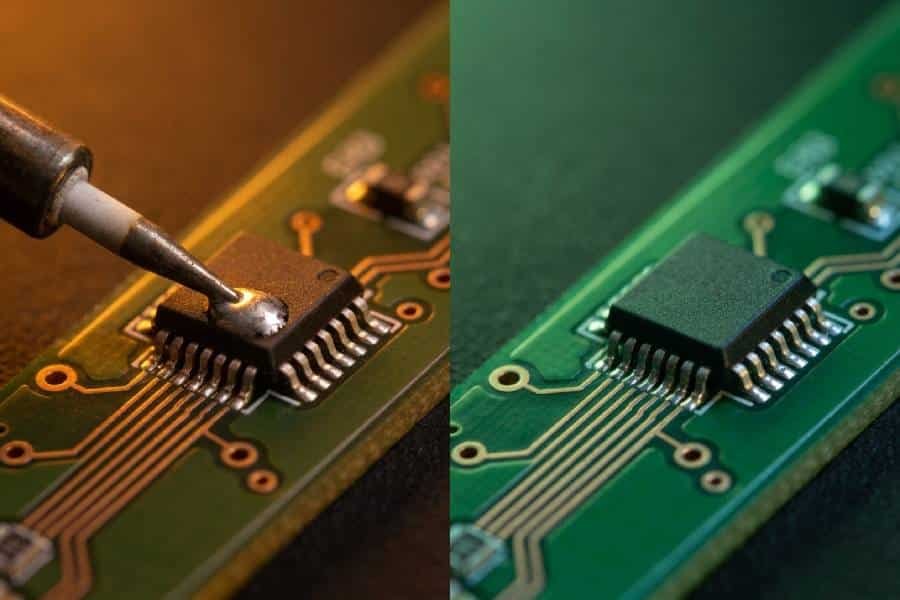
Wetting Behavior and Joint Appearance
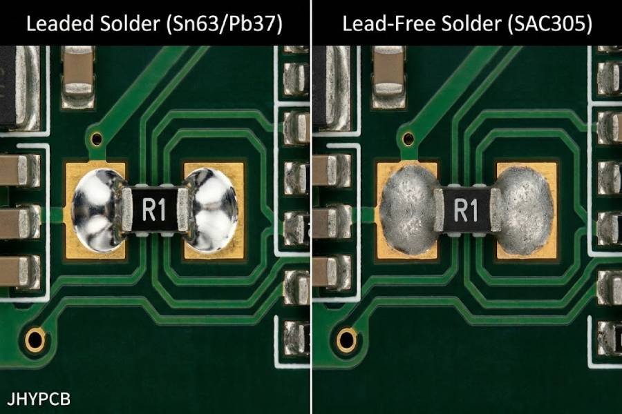
Leaded solder is well known for its excellent wetting and bright, shiny joint appearance, which makes visual inspection straightforward and tends to hide small process variations.
Lead-free solder often has less aggressive wetting and produces joints that look more matte or grainy, even when they are perfectly acceptable from an electrical and mechanical standpoint.
For assemblers and inspectors used to SnPb, this shift in appearance can take some adjustment, especially during the transition period when both types of joints may be present in the same facility.
It also means that lead-free processes generally benefit from tighter control of stencil design, solder paste handling, and reflow profiles to achieve consistent wetting and avoid voids, insufficient solder, or cosmetic rejects.
Process Window and Ease of Assembly
Because of its lower melting point and forgiving behavior, leaded solder offers a relatively wide process window and is often considered easier to work with, especially for hand soldering and rework.
Technicians can typically achieve good joints over a broader range of tip temperatures and contact times, and small deviations in profile or technique are less likely to produce marginal results.
Lead-free solder, on the other hand, usually demands more precise control of time and temperature during reflow, wave, and hand soldering to balance complete reflow against the risk of component or PCB damage.
In many factories, achieving yields with lead-free solder that match long‑standing leaded processes requires careful profile development, more disciplined process monitoring, and additional operator training—but once those steps are in place, lead-free can be run very consistently in volume production.
Reliability Considerations
Mechanical Strength and Fatigue Behavior
From a purely mechanical standpoint, lead-free solder joints often show higher tensile or shear strength than traditional tin–lead joints, at least in initial testing.
However, lead-free alloys tend to be more brittle, while leaded solder remains more ductile and better able to absorb shock and vibration without cracking, which can be an advantage in some high‑stress environments.
In practice, this means that lead-free joints may perform very well under static loading but can be more sensitive to certain combinations of mechanical shock, vibration, and thermal cycling if pad design, alloy choice, and assembly profiles are not carefully optimized.
Leaded joints, by contrast, are often more forgiving in older designs that were never tuned for the different mechanical behavior of lead-free alloys.
Thermal Cycling and High-Temperature Performance
Thermal cycling is one of the key stress factors for solder joints in many real‑world applications, from automotive and industrial control to outdoor infrastructure.
Studies comparing leaded and lead-free solder joints under thermal shock and long‑term cycling show a mixed picture: in some conditions lead-free performs as well or better, while in others the more ductile SnPb joints retain an advantage in crack resistance.
High-temperature aging also affects each alloy family differently.
Lead-free joints can develop thicker intermetallic compound (IMC) layers over time, which may influence crack paths and long‑term reliability, while leaded joints age more slowly but cannot be used where RoHS or similar regulations prohibit lead.
For new designs moving into lead-free PCB assembly, the safest approach is usually to combine appropriate alloy selection with design‑for‑reliability practices and, where necessary, application‑specific reliability testing rather than assuming that either alloy is always superior.
Tin Whiskers, IMC Growth, and Long-Term Aging
Lead-free solders and finishes can bring additional long‑term considerations such as tin whisker growth and different IMC structures at solder interfaces.
Lead historically helped suppress whisker formation in some tin‑based finishes; without it, certain surface finishes and plating systems require more careful control or mitigation strategies to reduce whisker risk.
Intermetallic layer thickness and morphology at the solder–pad interface also evolve over time and with temperature exposure, and these changes can influence how and where cracks form if a joint eventually fails.
For high‑reliability or long‑lifecycle products, both leaded and lead-free assemblies benefit from thoughtful material choices, controlled profiles, and appropriate accelerated aging tests so that long‑term behavior is understood rather than assumed.
Cost and Manufacturing Implications
Material and Process Costs
On a pure materials basis, traditional leaded solder alloys have historically been less expensive than many lead-free formulations, especially those with higher silver content.
However, in modern PCB assembly, solder alloy cost is usually only one part of the picture; the total cost also reflects equipment requirements, energy use, and any additional process development work needed to support lead-free production.
Lead-free PCB assembly often involves higher peak reflow and wave solder temperatures, which can increase energy consumption and, over time, contribute to more wear on heaters, tips, and solder pots.
At the same time, many EMS providers have already absorbed these changes into their standard processes, so the cost difference seen by OEMs may be modest or primarily driven by alloy choice and specific reliability or certification requirements.
Equipment, Energy, and Maintenance
Running lead-free profiles means reflow ovens, wave solder systems, and selective soldering equipment must be capable of higher operating temperatures and tighter control.
This can influence initial capital decisions for new lines and may slightly shorten the service life of some components, such as soldering tips or nozzles, due to the more aggressive conditions.
In many factories, these differences are now part of normal operations, but they still matter when budgeting for new capacity, planning maintenance, or comparing the economics of keeping a dedicated leaded line for legacy products.
From an OEM perspective, it is worth understanding whether a potential assembly partner treats lead-free as the default process or as a special case that might carry different pricing or lead‑time implications.
Training, Rework, and Yield
On the human side, leaded solder is widely regarded as easier to hand‑solder and rework because of its lower melting point, smoother flow, and more immediately readable joint appearance.
Lead-free solder typically requires more training for technicians to manage tip temperatures, dwell times, and inspection criteria, especially when transitioning from an all‑leaded environment.
During the early stages of a lead-free conversion, it is common to see more process tuning and trial builds as profiles and stencil designs are refined.
Once those parameters are dialed in, mature lead-free lines can achieve yields comparable to leaded processes, but reaching that point does demand more disciplined process control and documentation than many older SnPb setups ever needed.
Application Examples: When Lead vs. Lead-Free Makes Sense
Consumer and Export Products Under RoHS/REACH
For most high‑volume consumer electronics and any product shipped into markets that enforce RoHS or similar regulations, lead-free solder is effectively mandatory.
In these cases, the choice is less about personal preference and more about selecting suitable lead-free alloys, PCB materials, and assembly processes that can deliver the required reliability at an acceptable cost.
Even when some exemptions exist, many OEMs choose to standardize on lead-free PCB assembly across a product family to simplify compliance, documentation, and global distribution.
For designers working in these sectors, the practical question is not “lead or lead-free?” but “which lead-free alloy and process strategy best fits this product’s performance and regulatory needs?”
Industrial, Automotive, and High-Reliability Applications
In industrial, automotive, aerospace, and other high‑reliability applications, the picture is more nuanced.
Many new designs in these sectors have moved to lead-free solder to align with broader regulatory and customer expectations, but they typically do so with extensive reliability testing, careful material choices, and specific qualification plans.
At the same time, some legacy platforms and specialized systems continue to use leaded solder under applicable exemptions, especially where long field experience with SnPb joints forms part of the risk and reliability argument.
When deciding between leaded and lead-free in these contexts, teams often weigh factors such as expected service life, operating environment, regulatory roadmap, and the company’s capacity to support detailed reliability and compliance documentation.
Prototyping, Service, and Non-Regulated Use Cases
Outside tightly regulated markets, leaded solder still plays a visible role in prototyping, lab work, and some service or repair operations.
Its lower melting point and more forgiving wetting behavior make it attractive for quick bring‑up, manual modifications, and rework on older designs originally built with SnPb.
However, even in these scenarios, safety and future compliance considerations matter.
Teams should be clear about where prototype decisions might lock in constraints for later RoHS-compliant production, and they should handle leaded solder with appropriate health, safety, and waste‑handling practices.
Choosing Between Lead and Lead-Free Solder for Your PCB Assembly
Key Questions to Ask About Markets and Regulations
Before comparing detailed reliability data or debating solder preferences, it helps to start with a few simple questions about where the product will be sold and which regulations apply.
If your target markets require RoHS or similar compliance—and most consumer and many industrial markets now do—then lead-free solder is effectively a baseline requirement rather than an option.
For products that fall under documented exemptions or are used in tightly controlled environments, teams still need to consider how long those exemptions are likely to remain in place and whether customers are comfortable with leaded assemblies from a policy and branding standpoint.
Answering these questions early keeps you from designing around a solder strategy that becomes difficult to support halfway through the product’s lifecycle.
Balancing Reliability, Cost, and Manufacturability
Once regulatory constraints are clear, the choice between leaded and lead-free solder becomes a matter of balancing reliability, cost, and manufacturability for the specific application.
Leaded solder may offer advantages in ease of assembly and certain mechanical behaviors, while lead-free solder aligns better with modern environmental expectations and global logistics—provided the materials and processes are properly engineered.
In many cases, the key question is whether you can achieve the required reliability with a lead-free process at an acceptable cost of materials, process development, and testing.
Where that answer is yes and regulations point toward lead-free, the long‑term benefits of standardizing on lead-free PCB assembly often outweigh the short‑term convenience of sticking with SnPb.
Working with Your PCB Assembly Partner to Decide
You do not have to make this decision in isolation.
An experienced PCB assembly partner can share practical data on how different alloys perform in their lines, what reliability results they have seen, and how costs and lead times compare between leaded and lead-free options for similar products.
Bringing your EMS provider into the conversation early—sharing performance targets, markets, and lifetime expectations—allows them to suggest suitable solder systems, profiles, and test strategies instead of simply quoting “leaded vs. lead-free” as a checkbox on a form.
That collaboration usually leads to a more defensible choice, whether you ultimately standardize on lead-free PCB assembly or maintain a mixed strategy for specific legacy or high‑reliability programs.
Conclusion
There is no single “best” answer in the debate between leaded and lead-free solder for PCB assembly—only choices that fit or conflict with a product’s regulatory, reliability, and cost realities.
Leaded solder still offers advantages in ease of use and certain mechanical behaviors, but lead-free solder has become the default for RoHS‑compliant PCB assemblies and can deliver comparable reliability when materials, design, and processes are properly aligned.
For designers and OEMs, the most robust approach is to start with market and regulatory requirements, then work through reliability expectations, lifecycle plans, and manufacturing capabilities before committing to a solder strategy.
Partnering with an experienced PCB assembly provider and treating solder selection as part of a broader design‑for‑manufacturability and design‑for‑reliability conversation will usually lead to better long‑term outcomes than choosing lead or lead-free solder on habit alone.