


Table of Contents
Intro
When you tick the “controlled impedance” option on a PCB quote form, you are doing much more than adding a nice‑to‑have feature to your board. You are asking the manufacturer to treat certain traces as precision transmission lines with a defined electrical behavior, not just copper routes that happen to connect two pins.
If your requirements are vague or incomplete, the factory has to guess what you really need, which often leads to extra emails, delayed lead times and, in the worst case, boards that do not behave as expected in the lab.
High‑speed digital interfaces, RF lines and fast edge‑rate clocks can be very unforgiving. A few ohms of unexpected impedance variation or a poorly documented differential pair can be enough to cause eye‑diagram collapse, random bit errors or EMI problems that are difficult and expensive to debug later in the project.
On the other hand, when your controlled impedance requirements are clear and complete, your PCB manufacturer can set up the right stackup, choose appropriate materials and tune the process to hit your targets with far fewer surprises.
This article walks you through what information a PCB manufacturer really needs to build impedance‑controlled boards correctly, how to document it in your fabrication notes and when to consider coupons and TDR reports. By following these guidelines, you reduce the risk of miscommunication and give your high‑speed design a much better chance of working the first time.
Explore our impedance control PCB fabrication service.
Why clear controlled impedance requirements matter
From the manufacturer’s point of view, “controlled impedance” is not a single switch they can turn on; it is a set of constraints that affects materials, layer stackup, trace geometry and process tolerances across the entire panel.
If those constraints are not defined precisely, the engineering team must either make assumptions based on their own experience or stop the job and ask for clarification, both of which cost time and may still miss your true intent.
Unclear or incomplete requirements typically lead to one of three outcomes. In the best case, the factory guesses correctly, but you still waste time on back‑and‑forth emails and drawing updates. In a more common case, the boards are produced but do not meet the real impedance needs of your design, forcing you to adjust terminations, lower data rates or respin the layout altogether.
In the worst case, the problem only shows up late in system integration or field testing, where fixing a signal integrity issue is far more expensive than specifying the right impedance details at the start.
Clear controlled impedance requirements have the opposite effect. They allow the PCB manufacturer to simulate or calculate the expected impedance on the proposed stackup, select suitable dielectric materials, define realistic tolerance windows and decide where coupons and TDR verification are needed.
This reduces engineering uncertainty, shortens pre‑production review and increases the likelihood that your first article boards will match both your impedance targets and your project schedule.
What PCB manufacturers need to know for controlled impedance
1. Target impedance values and line types
The first piece of information your PCB manufacturer needs is the target impedance in ohms for each controlled structure. Typical examples include 50 Ω single‑ended traces, 75 Ω for some video lines, and 90 Ω or 100 Ω differential pairs used in high‑speed serial interfaces and Ethernet links.
Specifying only “controlled impedance required” without numbers forces the factory to guess or push the question back to you, which wastes time and may still not match the real needs of your design.
In addition to the numeric value, you should clearly indicate the line type for each impedance requirement. At a minimum, distinguish between single‑ended traces, differential pairs and any special coplanar or RF transmission lines in your layout.
Whenever possible, note whether the structure is intended as a microstrip (outer layer with air above) or a stripline (buried between reference planes), because the required line width and dielectric thickness will be different for the same impedance target.
It also helps to list which specific nets or signal groups require control. For example, you might call out high‑speed clocks, SerDes lanes, DDR memory buses, LVDS links or RF feed lines by name, instead of simply marking entire layers as “controlled impedance.”
This allows the manufacturer to focus calculations, coupon design and TDR verification on the most critical paths instead of treating every trace as equally important.
2. Impedance tolerance and critical nets
An impedance target is incomplete without an associated tolerance window. For many applications, a starting point of around ±10% is realistic and aligns with what most PCB manufacturing processes can achieve economically on standard stackups.
If you require significantly tighter tolerances, you should expect a closer engineering review, potentially different materials or stackups and, in some cases, higher cost or longer lead time.
It is also useful to distinguish between “critical” and “non‑critical” impedance‑controlled nets. High‑speed serial links, timing‑sensitive clocks or RF front‑end traces may justify tighter limits or routine TDR verification, while other nets in the same design can often tolerate a slightly wider impedance window.
By clearly indicating which nets fall into each category in your fabrication notes, you enable the PCB manufacturer to prioritize process control and testing effort where it has the greatest impact on system performance.
Stackup and material information you should include
3. Layer stackup, copper weights and dielectric thickness
For controlled impedance, the PCB stackup is just as important as the trace geometry itself. Your manufacturer needs a clear view of how many layers your board has, in what order they are arranged and which layers act as reference planes for the impedance‑controlled traces.
At a minimum, you should provide a proposed layer stackup that shows each signal and plane layer, along with its function (signal, ground, power) and relative position in the stack.
Alongside layer order, include the intended copper weights and dielectric thicknesses between signal layers and their reference planes. The combination of copper thickness, dielectric constant and dielectric thickness is what ultimately sets the achievable impedance for a given trace width and spacing.
If you leave these values unspecified, the factory may substitute default materials and thicknesses that do not match the assumptions you made during your own impedance calculations or simulations.
Even if your stackup is not final, sharing your current proposal allows the manufacturer’s engineering team to check whether your targets are realistic and suggest adjustments. For example, they might recommend slightly different core or prepreg thicknesses, or alternative copper weights, to hit your target impedance without pushing the process to its limits.
If you need practical examples of stackups we commonly use for high‑speed designs, see our impedance control PCB fabrication capabilities.
4. Base materials and overall board thickness
Base material selection also matters for controlled impedance, especially at higher frequencies. Standard FR‑4 is often sufficient for many high‑speed digital applications, but its dielectric constant and loss characteristics vary between vendors and even between batches.
If your design operates at very high data rates or RF and microwave frequencies, you may need to specify high‑frequency laminates such as Rogers or hybrid stackups that combine FR‑4 with low‑loss materials on the most critical layers.
When you request controlled impedance, indicate whether you require a specific material grade or manufacturer, or if you are open to equivalent materials that meet certain dielectric and loss parameters. This gives the PCB house room to choose laminates that are available and cost‑effective while still supporting your impedance and signal integrity goals.
You should also state the overall finished board thickness and any mechanical or connector constraints that limit how much the stackup can be adjusted, because this can affect which combinations of cores and prepregs are practical.
How to document controlled impedance in your fabrication notes
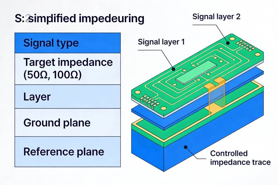
5. Impedance tables and layer references
Even if your impedance requirements are clear in your own mind, your PCB manufacturer still needs them expressed unambiguously in the fabrication drawing. One of the most effective ways to do this is to include a small impedance table that summarizes each controlled structure, its target value and the relevant layer references.
A typical table will list items such as “Signal type” (single‑ended or differential), “Target impedance in ohms,” “Routing layer,” “Reference plane layer” and any special notes about stackup or geometry.
For example, you might define entries like “100 Ω differential, routed on L3 over GND on L2” or “50 Ω single‑ended, microstrip on top layer over L2 ground plane.”
By writing the requirement in this structured way instead of burying it in free‑form comments, you make it much easier for the CAM engineer to match your intent to a practical stackup and trace geometry.
Where possible, keep your impedance table on the main fabrication drawing so that it is seen early in the engineering review, rather than as a note inside a separate document that might be overlooked.
If you have different impedance targets on multiple layers, group them clearly in the table and use consistent naming, so that each entry can be tied directly to the nets and layers in your design files.
6. Clear net naming and design file annotations
In addition to the fab drawing, your design files themselves should make it easy to identify which traces require controlled impedance. Meaningful net names for high‑speed interfaces, differential pairs and RF lines help the manufacturer cross‑refer your impedance table with the actual routing on the board.
Avoid generic names like “NET1_P” and “NET2_N” for critical differential pairs if you can; using names that reflect their function, such as “PCIE_TX1_P/N” or “ETH0_TX_P/N,” reduces the risk of confusion.
Some CAD tools also allow you to add impedance‑related notes directly in the layout or to assign specific rules to impedance‑controlled nets. While these internal rules do not replace a clear fabrication note, exporting them as part of your documentation package can give the CAM engineer valuable context about your intent.
Whatever method you use, the key is consistency: the nets called out in your impedance table should match the names in your schematic and layout, so the manufacturer does not have to guess which physical traces are supposed to meet each impedance target.
Testing, coupons and TDR reporting requirements
7. When to ask for coupons and TDR measurement
Specifying controlled impedance is one thing; verifying that the finished boards actually meet those targets is another. For many high‑speed and RF designs, especially those used in communication infrastructure, test and measurement are just as important as initial calculations.
If your product is safety‑critical, has tight compliance margins or will undergo formal qualification, you should consider asking your PCB manufacturer to include impedance coupons and Time Domain Reflectometry (TDR) testing as part of the build.
An impedance coupon is a small test structure placed on the production panel that contains representative traces for your controlled impedance nets. It is fabricated under the same process conditions as your boards, so its measured impedance provides a realistic picture of what is happening on the actual product.
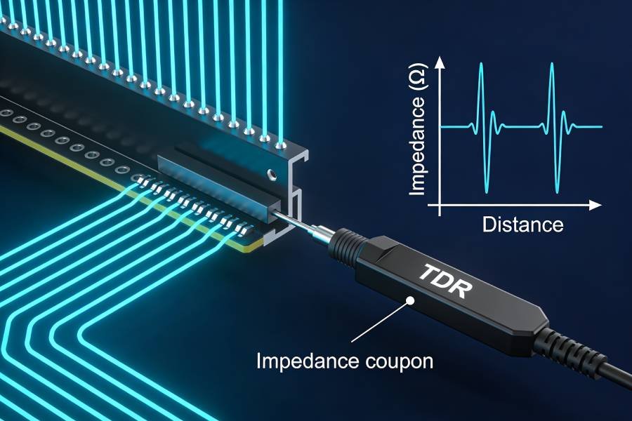
By clearly stating whether you need coupons and whether TDR testing is required on first articles only or on every batch, you help the manufacturer plan the appropriate process controls and test steps.
8. What to specify about impedance reports
If you request TDR testing, it is good practice to describe what kind of report you expect to receive. At a minimum, most engineers want to see the measured impedance values for each coupon structure, along with an indication of whether they fall within the agreed tolerance window.
Some manufacturers can also provide TDR plots and additional parameters, but asking for overly detailed or non‑standard formats may increase cost and lead time without adding much practical benefit.
When you define your reporting requirements, try to balance thoroughness with practicality. Focus on the high‑speed or RF nets where impedance is truly critical and be clear about which structures the TDR report should cover.
This targeted approach gives you the data you need to qualify your design, while allowing the PCB manufacturer to keep the testing process efficient and repeatable.
Common mistakes when specifying controlled impedance
Even experienced designers can run into problems when they first start working with controlled impedance requirements. Many issues do not come from the physics itself, but from gaps or ambiguities in the way those requirements are communicated to the PCB manufacturer.
Recognizing the most common mistakes makes it much easier to avoid them and to prepare a documentation package that supports a smooth fabrication process.
One frequent mistake is asking for “controlled impedance” without providing specific target values, line types or tolerance windows. A simple note like “all high‑speed traces to be impedance controlled” leaves too much room for interpretation and forces the factory either to guess or to stop the job to ask for more information.
A more effective approach is to clearly list which nets require 50 Ω single‑ended, which require 90 Ω or 100 Ω differential, and which structures are microstrips or striplines, together with realistic tolerances.
Another common problem is ignoring the stackup and material side of the requirement. Designers sometimes assume that specifying only trace width and spacing is enough, even when they are working with multilayer boards and mixed materials.
If the manufacturer chooses different dielectric thicknesses or laminate types than the ones you used in your calculations, the final impedance can easily drift outside the intended range, even if the trace geometry is held tightly.
A third mistake is treating every high‑speed net as equally critical and demanding the same tight impedance tolerance for all of them. While this may look safe on paper, it can increase cost and complexity without improving real‑world performance, because not all nets are equally sensitive to small impedance variations.
Separating truly critical interfaces from those with more margin allows you to focus process control and testing effort where it matters most, while keeping the overall build practical.
Finally, many issues arise simply because impedance requirements are added very late in the design or purchasing process. When controlled impedance is treated as an afterthought, stackup options may already be constrained by mechanical or cost decisions, and there is less flexibility to adjust materials or geometries.
Engaging your PCB manufacturer early, sharing preliminary stackups and targets and updating your fabrication notes before the design is frozen can prevent these last‑minute surprises and respins.
Working with your PCB manufacturer as a design partner
Controlled impedance is not just a checkbox on a quote form; it is a shared engineering problem that sits between your schematic, your layout and the manufacturer’s process capabilities.
Treating your PCB supplier as a design partner rather than a black box makes it much easier to arrive at a stackup and set of impedance targets that are both technically sound and manufacturable.
The most effective collaborations start early. Sharing preliminary stackups, target impedance values and key interface requirements before your design is completely frozen gives the manufacturer room to propose realistic material choices and geometry combinations.
In many cases, a brief review by an experienced CAM or signal integrity engineer can reveal opportunities to simplify the stackup, relax unnecessary constraints or tighten control only where it genuinely matters.
Once your documentation is ready, clear and consistent communication keeps the project on track. If the manufacturer raises questions about your impedance table, material selections or tolerance demands, treating those questions as part of a joint problem‑solving process rather than as obstacles helps ensure that the finished boards meet both your performance goals and your schedule.
Bringing it all together
Specifying controlled impedance is about more than writing a few numbers into a fabrication note. It means providing your PCB manufacturer with a complete picture of your targets, tolerances, stackup, materials, test expectations and priorities, so they can translate your design intent into a reliable physical product.
When you avoid common documentation mistakes and engage your supplier early, you greatly reduce the risk of signal integrity surprises, project delays and costly respins.
If you are preparing a new high‑speed or RF design and want support in defining or reviewing your controlled impedance requirements, our engineering team can help you refine your stackup, impedance table and test plan before fabrication.
To see how this works in practice and what capabilities are available, visit our Impedance Control PCB Fabrication service page and send us your Gerber files and impedance notes for a detailed review.


