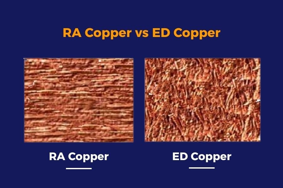
The Key Differences Between RA Copper and ED Copper in PCB Manufacturing: A Comprehensive Guide
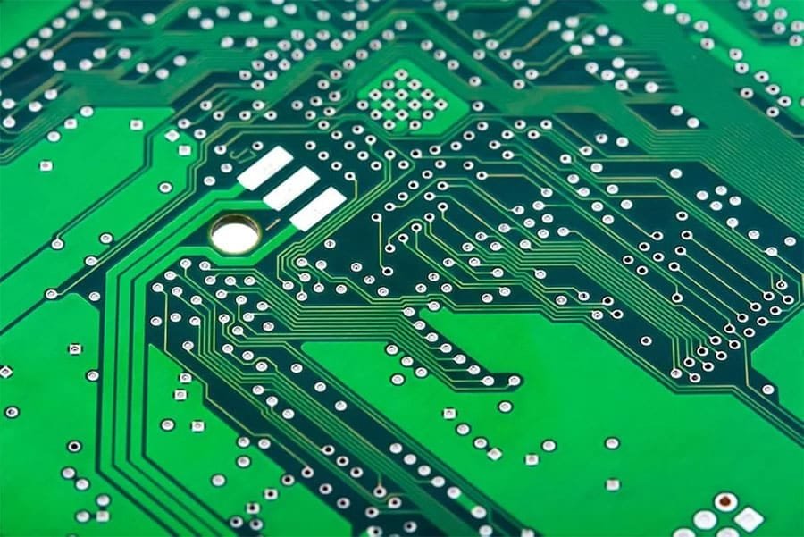
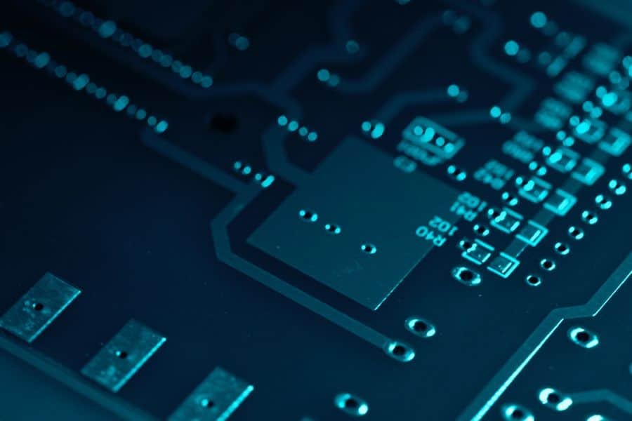
In PCB fabrication, especially for flexible circuits, the choice between RA copper and ED copper can make or break your design’s performance. This guide breaks down their structural differences, advantages in dynamic applications, and tips for optimizing your PCB assembly process.