
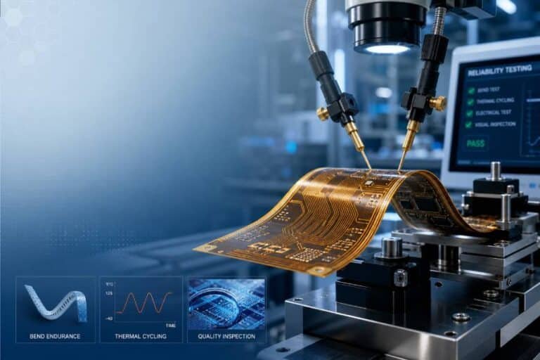
Flexible PCB Reliability Testing Standards and Methods
Flexible PCB reliability testing is essential for verifying bend life, thermal durability, and long-term electrical stability. This article explains the
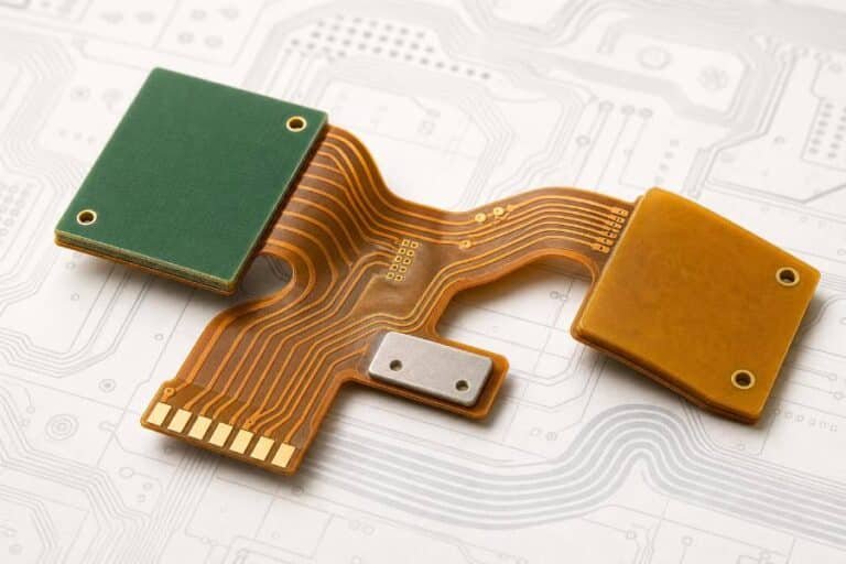
How to Choose the Right Stiffener for Flexible PCB Applications
This guide explains how to choose the right stiffener for flexible PCB applications based on connector needs, SMT assembly, bend
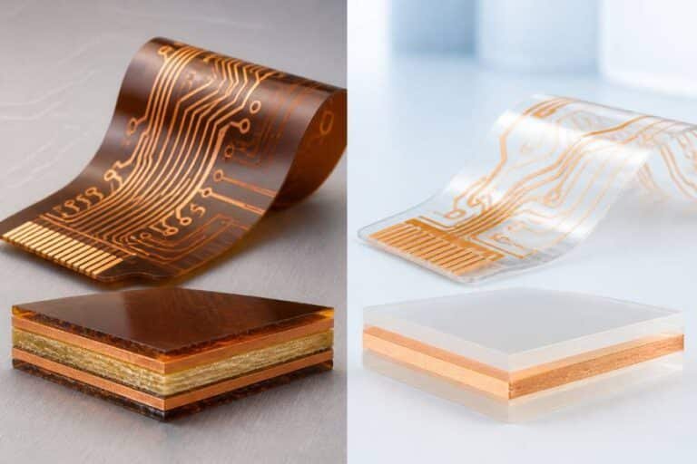
PI vs. PET in Flexible PCBs: Which Material Should You Choose?
Learn the key differences between PI and PET in flexible PCBs, including thermal performance, bend life, cost, and ideal use
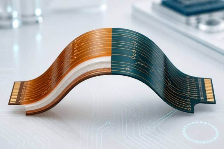
Adhesive vs. Adhesiveless Flex PCB: Which One Should You Choose?
Learn the key differences between adhesive and adhesiveless flex PCB, including construction, performance, cost, and the best use cases for
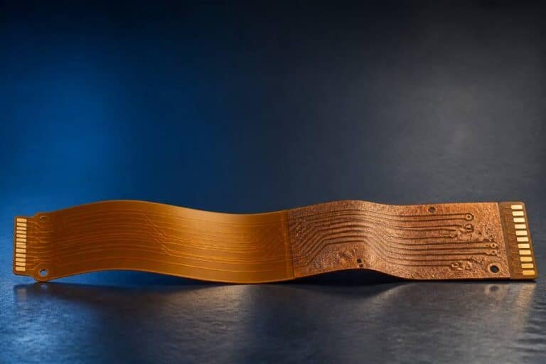
RA Copper vs. ED Copper in Flexible PCBs: Key Differences and Selection Guide
RA copper and ED copper serve different roles in flex PCB design. Learn which copper foil is better for dynamic
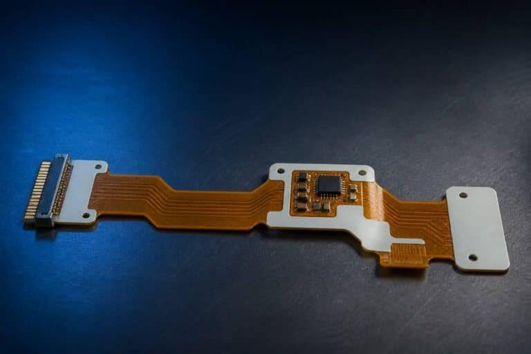
What Are PCB Stiffeners for Flexible Circuits? Materials and Uses
PCB stiffeners improve flex circuit reliability by reinforcing connector areas, supporting components, and adding local rigidity where flexible boards need
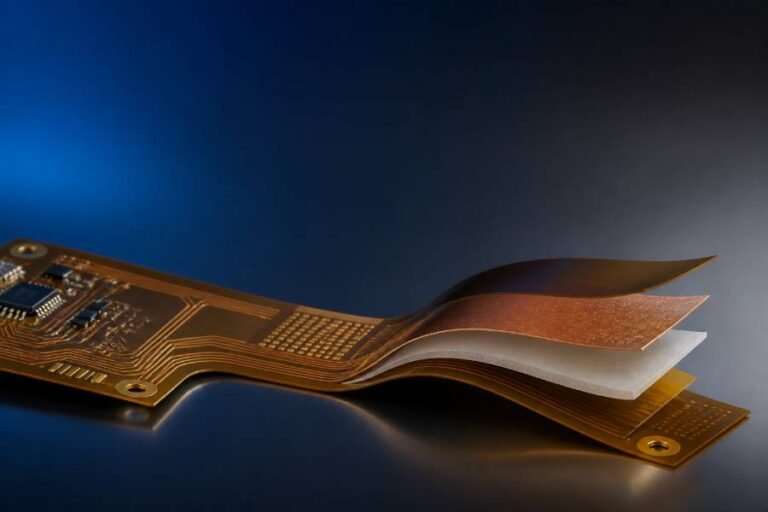
Flex PCB Adhesives and Bonding Materials Explained
Explore the main flex PCB adhesives and bonding materials used in flexible circuit construction, and see how each one affects
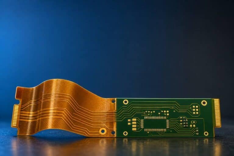
Flexible PCB Coverlay vs. Solder Mask: Which Protection Should You Choose?
A practical guide to flexible PCB coverlay vs. LPI solder mask, covering material differences, use cases, design considerations, and common
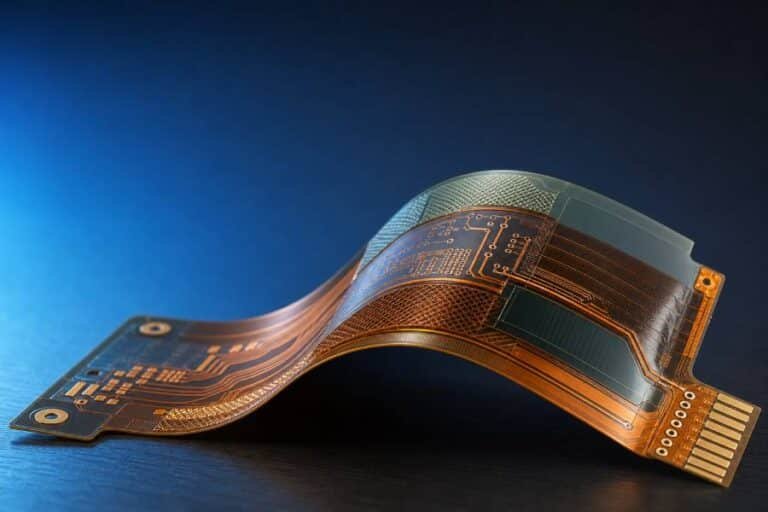
Flexible PCB Materials Guide: How to Choose PI, PET, Coverlay, and Adhesives for Reliable Designs
A practical guide to flexible PCB materials, covering PI vs. PET, coverlay, adhesives, copper layers, and stackup selection for reliable
RO4350B Dielectric Constant Explained: Parameters, Design Impact and Applications
This practical guide explains the RO4350B dielectric constant in real engineering terms—typical Dk and Df values, test conditions, design impact
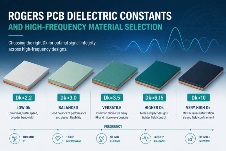
Rogers PCB Dielectric Constants Explained: Dk, Df and How to Choose High‑Frequency Materials
This practical guide walks through Rogers PCB dielectric constants—from Dk and Df basics to real‑world comparisons of RO4003C, RO4350B, RO3003
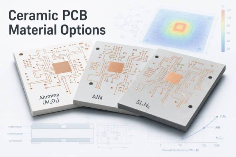
Alumina vs AlN vs Silicon Nitride: Choosing Ceramic Substrates for High-Power Electronics
This practical guide explains when to move from FR‑4 or MCPCBs to ceramic PCBs, compares key materials like alumina, AlN,

IC Substrate vs. PCB: A Practical Engineer’s Guide
IC substrates and printed circuit boards can look similar, but they are designed for very different jobs. An IC substrate

How to Choose the Best Multilayer PCB Fabrication Service Near You – And When to Go Overseas
Searching for a “multilayer PCB fabrication service near me” is only the first step. This guide shows you how to
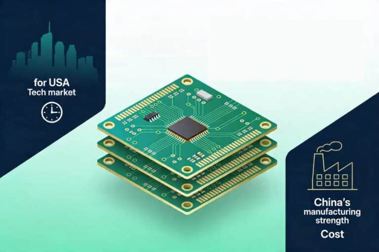
Where to Buy Multilayer PCBs with Quick Turnaround: Options in USA and China
Need multilayer PCBs fast but not sure whether to order from a local U.S. manufacturer or a China‑based supplier? This
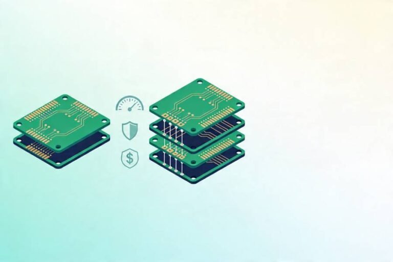
Multilayer PCB vs Double‑Sided PCB: Performance, Reliability and Cost Compared
Not sure whether your next design should stay on a double‑sided PCB or move to a multilayer stackup? This guide

Advantages of Multilayer PCB Design (and How Layer Count Impacts Cost from 2 to 10+ Layers)
Multilayer PCBs deliver better signal integrity, higher density, and more reliable power distribution than simple two‑layer boards—but they also affect

4 Layer PCB Manufacturing Process: Step‑by‑Step Guide from Inner Layers to Final Testing
This guide walks you through the full 4 layer PCB manufacturing process step by step—from FR4 material preparation and inner