Table of Contents
When you look at a high‑density electronic assembly, it is easy to confuse an IC substrate vs. PCB because both use copper traces on insulating materials to connect electronic functions. In reality, an IC substrate sits directly under the bare chip and handles ultra‑fine interconnects inside the package, while the printed circuit board (PCB) connects that packaged device to the rest of the system. Understanding how IC substrates and PCBs differ in structure, materials, manufacturing, performance, and cost is essential for engineers and sourcing teams making decisions about advanced packaging and system design.
Why People Confuse IC Substrates and PCBs
Similar roles at first glance: interconnection and support
At a quick glance, IC substrates and PCBs look like similar products: both are flat structures made of copper and dielectric materials that provide electrical interconnection and mechanical support for components. In both cases, designers route signals, power, and ground across multiple layers, define stack‑ups, and care about impedance, reliability, and manufacturability. This visual and functional similarity often leads people to assume that IC substrates are just “very fine PCBs” or that PCBs could directly replace substrates in most designs.
Where IC substrates and PCBs sit in the system hierarchy
The key difference is where each technology sits in the electronic system hierarchy. An IC substrate operates at the package level, directly under a bare die or multiple dies, and is responsible for fanning out tiny chip pads into a solderable pattern such as a BGA ball grid. A PCB, by contrast, works at the system or board level, connecting many packaged devices—processors, memories, sensors, connectors, power stages—across a larger area and often across the entire product. Recognizing this difference in function and scale is the first step toward understanding why IC substrates and PCBs are designed, manufactured, and specified in very different ways.
What Is an IC Substrate? (Quick Recap)
Package‑level interposer under the bare die
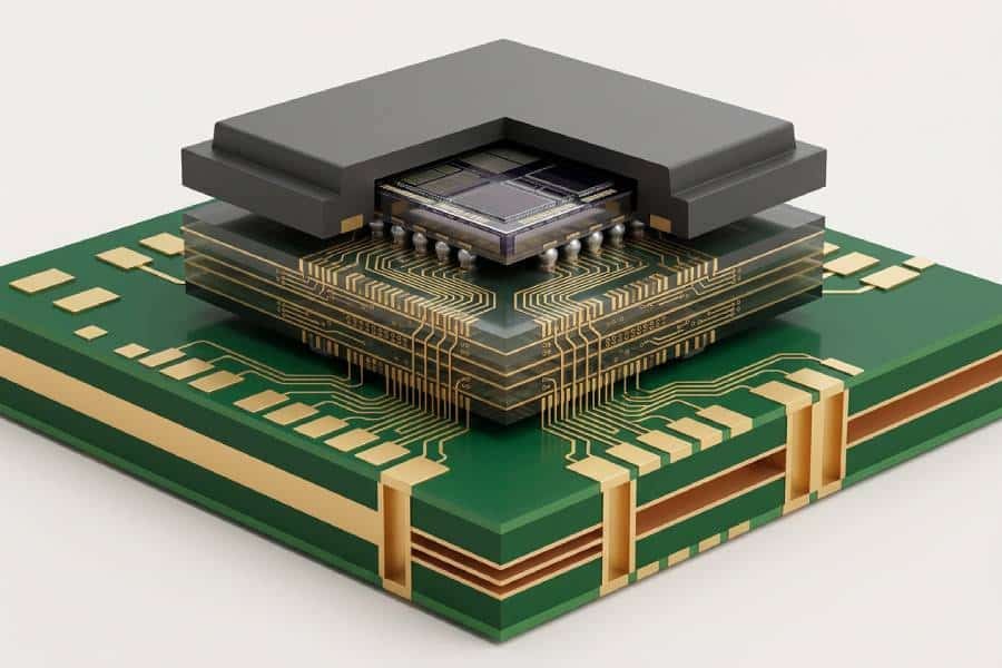
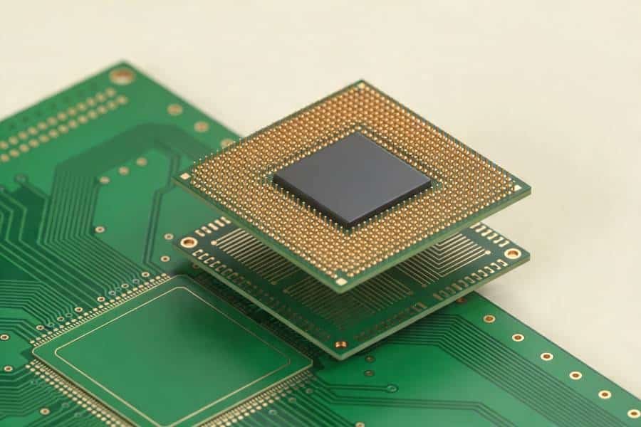
An IC substrate is a package‑level interposer that sits directly under a bare semiconductor die and bridges the gap between nanometer‑scale chip features and millimeter‑scale PCB traces. It receives tiny pads or bumps from the die on its top side and fans them out through fine traces and vias to a larger array of solder balls or leads on its bottom side, which can then be mounted onto the printed circuit board.
Core functions: high‑density routing, support, thermal path
Functionally, the IC substrate provides high‑density electrical routing, mechanical support for the die, and an important thermal path out of the chip. Its multilayer stack‑up, materials, and layout are engineered to manage signal integrity, power delivery, and heat flow within the package, often using advanced materials such as ABF or BT resin, and in some cases ceramic or glass cores. Because it operates so close to the die, the IC substrate is a critical part of overall package performance and reliability, not just a simple mounting surface.
What Is a PCB in Comparison?
System‑level interconnect platform for multiple components
A printed circuit board (PCB) is the system‑level interconnect platform that ties together many packaged components—processors, memory devices, connectors, sensors, power stages, and more—across a larger physical area. Instead of sitting directly under a bare die, the PCB receives fully packaged ICs and modules on its surface and routes signals, power, and ground between them to implement the complete electronic system. It also provides mounting points, connectors, mechanical support, and often interfaces with enclosures, heat sinks, and cabling.
Typical PCB structures and feature sizes
Structurally, PCBs are usually built from glass‑reinforced epoxy laminates such as FR‑4 or from specialized high‑speed, high‑frequency, or metal‑core materials depending on application needs. They use thicker dielectrics, larger vias, and coarser line/space than IC substrates, because they must span longer distances, carry higher currents, and manage manufacturability and cost at the system level. While advanced PCBs can certainly support fine‑pitch BGAs and high‑speed routing, their feature sizes and tolerances are generally less aggressive than those found inside IC packages.
IC Substrate vs. PCB: Structural and Geometrical Differences
Size, thickness, and integration level
IC substrates are physically much smaller than PCBs and are designed to match the footprint of one die or a small group of dies, plus a margin for routing and solder ball arrays. They are typically thin, with tightly controlled thickness to support short interconnect paths and precise impedance within the package. PCBs, by contrast, span the entire system or product outline and must support many components, connectors, and mechanical features, so they are larger, thicker, and structurally optimized for rigidity and mounting rather than extreme miniaturization.
Line/space, via size, and routing density
Geometrically, IC substrates operate at much finer line/space and via sizes than most PCBs. Substrates often use build‑up layers with very thin dielectrics, fine copper traces, and laser‑drilled microvias to fan out dense bump arrays from the die. This enables extremely high routing density in a small area, but also requires tighter fabrication tolerances and more advanced processes. PCBs can support fine‑pitch BGA escape routing, but their typical line/space and via sizes are larger, tuned for manufacturability, yield, and cost over bigger panel areas rather than maximum density under a single chip.
Stack‑up design and layer count considerations
Stack‑up design also differs significantly between IC substrates and PCBs. A substrate stack‑up is usually optimized around the die and package requirements, using multiple build‑up layers near the chip to manage high‑speed signals, power planes, and reference layers within a short vertical distance. Layer counts can be high relative to the small substrate area, with careful attention to warpage, via reliability, and material interactions. PCB stack‑ups, on the other hand, are sized to support system‑level routing across the entire board, often combining high‑speed layers, power distribution layers, control and low‑speed layers, and sometimes thicker cores or metal planes for mechanical and thermal reasons.
IC Substrate vs. PCB: Material Differences
IC substrate materials (ABF, BT resin, ceramic, glass)
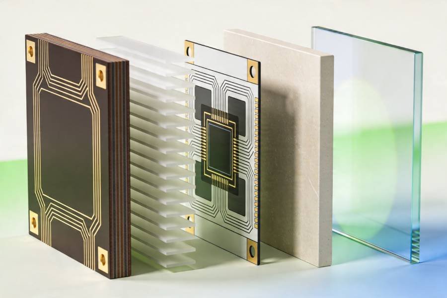
IC substrates typically use higher‑performance materials than mainstream PCBs because they sit directly under the die and must support very fine features and demanding reliability targets. Common organic systems include BT resin and Ajinomoto Build‑up Film (ABF), which are formulated for fine‑line routing, laser‑drilled microvias, controlled dielectric behavior, and good thermal stability in advanced packages. For high‑power or harsh environments, ceramic substrates based on alumina or aluminum nitride, and emerging glass core substrates, provide improved thermal conductivity, dimensional stability, and—in the case of glass—very low loss and tight dimensional control for high‑frequency applications.
PCB materials (FR‑4, high‑speed laminates, metal core, others)
PCBs, by comparison, rely primarily on glass‑reinforced epoxy systems such as FR‑4 for general‑purpose designs, with a broad range of high‑speed, high‑frequency, and metal‑core laminates used where needed. FR‑4 and related materials are optimized for cost, manufacturability, and adequate performance across many applications, rather than the extreme density and proximity to the die seen in IC substrates. For boards that must carry high‑speed or RF signals, designers may specify low‑loss laminates or hybrid stack‑ups that blend FR‑4 with specialized high‑frequency materials, but even these are generally designed around system‑level routing and assembly rather than package‑level constraints.
Why material choices diverge at package vs. board level
The divergence in materials between IC substrates and PCBs reflects their different roles and constraints. At the package level, materials must support ultra‑fine geometries, tight thickness control, and close proximity to local hot spots and thermal cycles at the die, driving the use of ABF, BT, ceramics, or glass with carefully tuned dielectric, thermal, and mechanical properties. At the board level, materials must be available in larger panel sizes, support thicker constructions, manage higher currents and mechanical loads, and remain cost‑effective across the entire product, which is why FR‑4 and system‑optimized laminates dominate PCB designs. Understanding these material differences helps explain why an IC substrate generally cannot be replaced by a standard PCB, even though both use copper and dielectric layers to provide interconnection and support.
IC Substrate vs. PCB: Manufacturing and Process Differences
Substrate fabrication: build‑up layers, microvias, tight tolerances
IC substrate fabrication relies heavily on build‑up processing, where thin dielectric films and copper layers are sequentially laminated, imaged, and etched to create very fine routing near the die. Laser‑drilled microvias, stacked via structures, and tight layer‑to‑layer registration are standard, because substrates must fan out dense bump arrays within a small footprint. Process windows are narrow, with strict control over thickness, via quality, and warpage to maintain yield and reliability at package level.
PCB fabrication: larger panels, coarser features, cost optimization
PCB manufacturing, while also using multilayer lamination, drilling, and imaging, is optimized for larger panel sizes, coarser features, and cost‑effective production across many board shapes and designs. Mechanical drilling remains common for through‑holes and vias, and although laser drilling and HDI techniques are used for fine‑pitch BGAs, the overall feature sizes and tolerances are looser than those typical in IC substrates. PCB processes are tuned to deliver consistent quality and acceptable yields at lower cost per unit area, rather than to push the absolute limits of density under a single die.
Impact on yield, lead time, and manufacturability
These process differences have direct implications for yield, lead time, and manufacturability. Because IC substrates use finer geometries, thinner dielectrics, and complex microvia structures, they are more sensitive to small variations in imaging, drilling, plating, and lamination, which can impact yields and require more stringent process control. Lead times for advanced substrates can also be longer, especially when using materials like ABF, ceramics, or glass that are processed in more specialized facilities.
PCBs benefit from more mature, high‑volume manufacturing ecosystems, which can offer shorter lead times and lower costs for a wide range of designs, especially when using standard FR‑4 or common high‑speed laminates. However, as PCB designs adopt more HDI and advanced materials, the gap between board‑level and substrate‑level complexity is narrowing, making early collaboration with fabricators important for both domains.
Performance Comparison: Signal Integrity, Power, and Thermal Behavior
High‑speed and high‑frequency signaling on substrates vs. boards
At high data rates and RF frequencies, the IC substrate is the first and often most critical segment of the signal path leaving the die. Very short trace lengths, fine geometries, and carefully controlled stack‑ups on the substrate help manage impedance, reduce parasitics, and minimize reflections and loss in the immediate vicinity of the chip. The PCB then continues those high‑speed routes over longer distances, usually with slightly coarser features and different materials, so both substrate and board must be co‑designed to meet overall signal‑integrity budgets.
Power delivery paths from die through substrate to PCB
For power delivery, the IC substrate provides the local distribution network between the die bumps and the solder balls or leads that connect to the PCB. Power and ground planes within the substrate, along with decoupling strategies near the die, strongly influence voltage droop, noise, and current distribution at the package level. The PCB then supplies bulk power, larger copper areas, and additional decoupling to support the entire system, so its stack‑up, plane design, and via structures must align with the substrate’s PDN to avoid bottlenecks or resonances.
Thermal management roles of substrates and PCBs
Thermally, the IC substrate helps conduct heat away from local hot spots on the die toward solder balls, copper planes, heat spreaders, or other thermal paths. Its material system—whether ABF, BT, ceramic, or glass—affects how efficiently heat moves out of the package and how much warpage or stress develops during temperature changes. The PCB contributes by providing additional copper area, thermal vias, and interfaces to heat sinks, chassis, or ambient, so its design is crucial for system‑level temperature control. Effective thermal management in modern products therefore depends on treating the IC substrate and PCB as a combined thermal path rather than isolated elements.
Reliability and Qualification: Package‑Level vs. System‑Level Stress
Package‑level reliability: bumps, microvias, and local hot spots
At the package level, IC substrates face reliability challenges that are very close to the die: solder bumps, microvias, thin dielectrics, and local hot spots all experience repeated thermal and mechanical stress during operation and assembly. Thermal cycling, power on/off events, and non‑uniform heating can drive fatigue in microvias, cracks in dielectric layers, and stress at the die‑to‑substrate interface, especially when CTE mismatches exist between silicon, substrate materials, and underfill. Package‑level qualification therefore focuses heavily on bump reliability, via robustness, warpage control, and resistance to delamination around the die and within the substrate stack‑up.
Board‑level reliability: solder joints, connectors, and environment
At the system level, PCBs see a different set of reliability stresses. Solder joints between the PCB and packaged components must survive vibration, shock, bending, and thermal cycling across the entire assembly, often over larger temperature ranges in automotive, industrial, or outdoor equipment. Connectors, cables, and mechanical mounting points on the PCB also contribute to stress distribution and potential failure points under real‑world conditions. Board‑level qualification tends to emphasize solder joint reliability, via and pad robustness, environmental resistance (humidity, corrosion), and overall mechanical durability of the assembled product
How IC substrate and PCB choices interact in real products
In practice, IC substrate and PCB reliability are tightly linked, because failures at either level can compromise the same system. A robust package on a marginal PCB, or a strong PCB hosting a marginal package, both increase overall product risk. Material choices, stack‑ups, and design rules for the substrate and board need to be considered together, particularly for automotive, industrial, and high‑reliability applications where system‑level qualification is stringent. By co‑optimizing IC substrate and PCB designs, teams can better manage combined thermo‑mechanical stresses and reduce the likelihood of unexpected failures during qualification or in the field
Cost and Design Trade‑offs Between IC Substrates and PCBs
Cost drivers for substrates vs. boards
The main cost drivers for IC substrates are advanced materials, fine geometries, and tight process control. ABF or BT resin systems, thin build‑up layers, laser‑drilled microvias, and stringent warpage and registration requirements all contribute to higher cost per unit area than typical PCBs. PCB cost, by contrast, is driven more by panel utilization, layer count, via complexity, special laminates, and overall board size, with economies of scale available through mature high‑volume manufacturing.
When advanced substrates are necessary—and when they are not
Advanced IC substrates are necessary when a design requires very high I/O density, tight flip‑chip bump pitches, complex power delivery networks, or high‑speed interfaces that cannot be handled directly on a PCB. In these cases, trying to avoid a substrate by using only a board‑level solution would either be impossible or would severely limit performance and integration. On the other hand, simpler devices and modules that use lower pin counts, moderate speeds, or standard packages can often rely on conventional PCBs without the need for an intermediate IC substrate layer.
Balancing performance, reliability, and budget
For most projects, the decision is not “IC substrate or PCB” but rather “what combination of IC substrate and PCB technologies best meets our performance and cost targets.” High‑end systems may justify expensive substrates and specialized board materials to reach their performance goals, while mid‑range products can use more cost‑effective substrates and standard PCBs with carefully chosen stack‑ups. Early cost modeling and technical evaluation with both substrate and PCB manufacturers help teams avoid over‑specifying one layer while under‑investing in the other, leading to a more balanced and economical overall design.
When Do You Need an IC Substrate? When Is a PCB Enough?
Typical use cases for IC substrates (CPUs, AI, 5G, automotive, etc.)
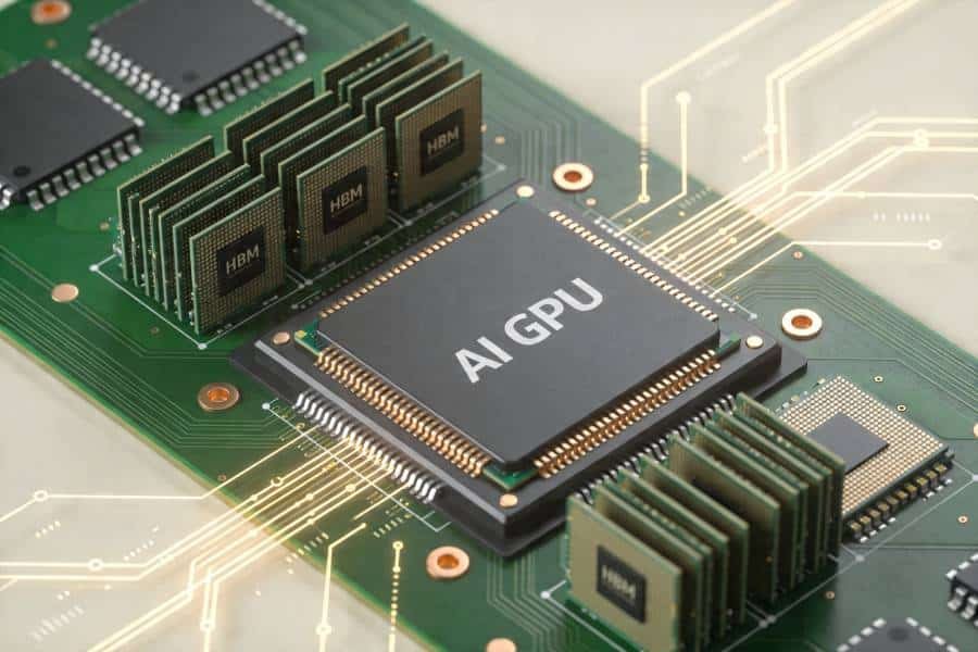
IC substrates are typically required in advanced semiconductor packaging where bare dies must be interconnected at very high density and performance. Common examples include CPUs, GPUs, AI accelerators, high‑end networking ASICs, high‑bandwidth memory, RF front‑end modules, and many automotive and industrial controllers that use flip‑chip or fine‑pitch BGA packages. In these applications, the substrate is an integral part of achieving the necessary I/O count, signal integrity, power delivery, and thermal management.
Cases where a standard PCB or simple module is sufficient
For simpler devices and lower‑complexity systems, a standard PCB or modest HDI board may be sufficient without a dedicated IC substrate. Examples include many analog and power circuits, low‑to‑mid‑speed microcontrollers, discrete component assemblies, and modules where packaged ICs can be connected directly on the board without requiring an internal package‑level interposer. In such cases, adding an IC substrate would increase cost and complexity without delivering meaningful benefits.
Hybrid approaches: modules, SiP, and system‑level thinking
Between these extremes, hybrid approaches such as system‑in‑package (SiP), multi‑chip modules, and advanced board‑level modules combine IC substrates and PCBs in creative ways. A design may use one or more IC substrates to integrate critical high‑speed or high‑power functions, then mount those packages on a PCB that handles system‑level connectivity and mechanical integration. Thinking about IC substrates and PCBs together—rather than as isolated technologies—allows engineers to partition functions where they make the most sense in terms of performance, reliability, and cost.
Working with Your Manufacturer on Substrate and PCB Choices
Co‑design between chip, substrate, and PCB
As packaging and system complexity increase, co‑design between the chip, IC substrate, and PCB becomes more important. Decisions about bump maps, substrate stack‑ups, via structures, and PCB layer assignments all affect signal integrity, power delivery, thermal behavior, and manufacturability. Aligning design rules and performance targets across these three levels early in the project helps avoid costly rework and improves the chances of first‑time‑right prototypes.
What to discuss with IC substrate manufacturers
When working with an IC substrate manufacturer, engineers should share package outlines, die bump maps, target interfaces, thermal requirements, and reliability expectations, rather than focusing only on basic drawings or GERBER data. This allows the supplier to recommend appropriate substrate materials (ABF, BT, ceramic, glass), stack‑ups, and via strategies that match both their process capabilities and the project’s performance goals. Process window information—such as minimum line/space, via sizes, and panel formats—can then be used to refine the design iteratively.
How PCB manufacturers support substrate‑level decisions
PCB manufacturers also play a role in IC substrate decisions, particularly when high‑speed interfaces, power delivery, or thermal paths cross the package‑to‑board boundary. By sharing board‑level stack‑ups, materials, and design rules with packaging teams, PCB fabricators help ensure that substrate and board designs are compatible in terms of impedance, loss, CTE behavior, and assembly processes. In some cases, PCB and substrate suppliers may collaborate to propose combined solutions—such as specific material pairs or via strategies—that optimize overall system performance and manufacturability.
Summary: IC Substrate vs. PCB in One View
Quick checklist for choosing technologies
A simple way to think about IC substrate vs. PCB is to ask a few key questions:
- Does the design require bare‑die or multi‑die integration with very high I/O density?
- Are data rates, frequencies, or power densities high enough that package‑level routing and materials will strongly affect performance?
- Are environmental and reliability conditions demanding enough to warrant specialized substrate materials and processes?
If the answer to these questions is “yes,” an IC substrate is likely required; if not, a well‑designed PCB or module may be sufficient.
How this decision affects future scaling and product roadmaps
Choosing how to partition functions between IC substrates and PCBs has long‑term implications for product scaling and roadmaps. Designs that adopt suitable substrate technology early may find it easier to scale pin counts, data rates, or power levels in future generations, while staying within acceptable board‑level complexity. Conversely, trying to work around package‑level limitations purely at the PCB level can make later scaling more difficult and expensive. For teams planning advanced products, it is worth discussing IC substrate options with experienced manufacturing partners—especially those offering IC substrate manufacturing services in China—so that chip, substrate, and PCB choices support both current requirements and future product evolution.