Table of Contents
When you look inside modern electronic devices, there is usually an important layer between the bare chip and the main printed circuit board (PCB) called an IC substrate. It acts as a high‑density carrier that routes fine‑pitch signals from the semiconductor die to the larger PCB traces, while also helping to deliver power and manage heat. Understanding what an IC substrate is and how it works is essential for engineers and sourcing teams who are involved in advanced packaging, high‑speed design, or selecting the right manufacturing partner for complex electronic products.
IC Substrate Definition and Core Functions
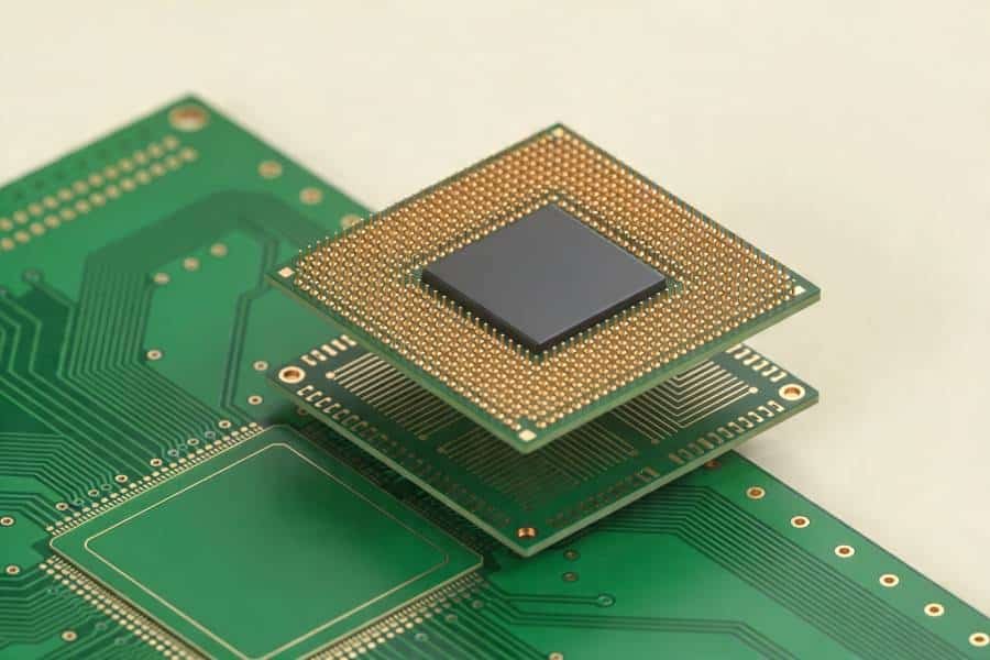
At the most basic level, an IC substrate is a specially designed base that sits between a bare semiconductor die and the main PCB, acting as a bridge between nanometer‑scale chip features and millimeter‑scale board traces. It provides a finely patterned interconnect platform so that tiny die pads can be fanned out into a larger, more manageable array of solder balls or leads. In other words, the IC substrate converts the chip’s extremely dense I/O into a format that can be reliably assembled onto a printed circuit board.
Structurally, an IC substrate is typically a multilayer build‑up circuit board made from high‑performance organic materials such as BT resin or ABF, and in some cases ceramic or glass‑based materials. Inside this thin package carrier are multiple copper layers, microvias, and carefully controlled trace geometries that are optimized for electrical performance, thermal behavior, and mechanical stability. The substrate must be thin and dense enough to support modern packaging requirements, while still robust enough to survive assembly and operating conditions over the product’s lifetime.
From a functional perspective, the IC substrate has several core roles in advanced electronic packaging. First, it provides electrical interconnection between the semiconductor die and the system‑level PCB by routing high‑density signals, power, and ground through fine traces and vias. Second, it offers mechanical support, holding the chip in place and forming the structural base of the package so that it can be reliably mounted on the end product board. Third, it contributes to thermal management by helping conduct heat away from the die toward larger copper areas, heat spreaders, or the surrounding system.
In addition to these primary functions, the IC substrate also plays a role in controlling signal integrity, power integrity, and electromagnetic behavior within the package. Its layer stack‑up, material selection, and routing strategy all influence timing, impedance, crosstalk, and noise, which become especially critical in high‑speed, high‑frequency, or high‑pin‑count designs. Because of this, many engineers now view the IC substrate not just as a mechanical base, but as an integral part of the overall electronic design that must be co‑optimized with the chip and the PCB.
IC Substrate vs. Traditional PCB
Because an IC substrate looks similar to a very fine‑pitch circuit board, it is common to compare IC substrates vs. PCBs and ask whether they are essentially the same thing. In reality, they share some basic functions but are designed for different levels of the electronic system. Both structures provide electrical interconnection, insulation, and mechanical support for components, but an IC substrate works at the package level, while a traditional PCB operates at the system or board level.
A traditional PCB is designed to connect many packaged components—such as processors, memory, connectors, and power devices—across a larger board area. It usually uses coarser line widths and spacings, larger vias, and cost‑optimized materials like FR‑4 or related laminates. The PCB focuses on routing signals across the entire system, managing power distribution, and providing a robust mechanical platform that can be mounted into an enclosure or end product. Design rules are strict, but generally more forgiving than those used in IC packaging substrates.
An IC substrate, by contrast, is a much smaller, high‑density interconnect platform that sits directly under a bare die or multiple dies. It uses much finer line/space, smaller microvias, and tighter dimensional tolerances, because it must fan out the tiny pads on the chip into a solderable pattern such as a BGA ball grid. Materials are often higher performance, such as BT resin, ABF build‑up films, ceramic, or even glass core technologies, chosen specifically for their electrical, thermal, and reliability characteristics in advanced packaging.
There are also important differences in manufacturing complexity and cost between an IC substrate and a standard PCB. IC substrates typically require more imaging steps, finer registration control, laser‑drilled microvias, and stricter warpage management than most system‑level PCBs. As a result, they are more challenging to fabricate and usually more expensive per unit area, but they enable package designs that would not be possible with conventional board technology alone. PCBs, on the other hand, are optimized to balance performance, manufacturability, and cost across a wide range of applications.
From a reliability perspective, both IC substrates and PCBs must survive environmental stress, but the stress profiles and failure modes can differ. IC substrates are subjected to repeated thermal cycling right at the chip level, local hot spots, and package‑level mechanical strains, so their materials, stack‑ups, and vias are engineered to minimize cracking, delamination, and interconnect fatigue in the immediate vicinity of the die. System PCBs also face temperature changes, vibration, and mechanical loading, but their design margins, feature sizes, and material choices give them more flexibility to accommodate these effects over a larger physical area.
A useful way to think about the relationship between an IC substrate and a PCB is to see them as two levels of a single interconnect hierarchy. The IC substrate bridges the microscopic world of the semiconductor die to the mesoscopic world of the printed circuit board, and the PCB then connects that package to the rest of the system—power supplies, connectors, memories, sensors, and peripheral circuitry. Understanding how these two layers differ, and how they work together, is essential when choosing materials, defining stack‑ups, or selecting manufacturing partners for advanced electronic products.
IC Substrate Materials and Structures
Because an IC substrate operates so close to the semiconductor die, its materials and internal structure have a direct impact on electrical performance, thermal behavior, and long‑term reliability. Most IC substrates used in advanced packaging are multilayer build‑up circuit boards made from high‑performance organic or inorganic materials, with carefully engineered copper features and via structures.
One common class of IC substrate materials is organic laminates based on BT resin and ABF (Ajinomoto Build‑up Film) systems. BT resin substrates are widely used in high‑reliability packages because they offer a good balance of thermal stability, electrical properties, and mechanical strength. ABF build‑up materials support very fine line/space and multiple build‑up layers, making them suitable for high‑density interconnect structures in CPUs, GPUs, networking ASICs, and other high‑pin‑count devices.
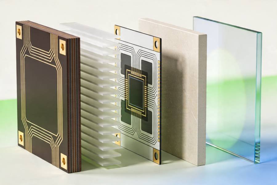
In addition to organic materials, some IC substrates use ceramic or glass‑based constructions for more demanding applications. Ceramic substrates, such as LTCC or HTCC, provide excellent thermal conductivity, dimensional stability, and high‑temperature performance, which are beneficial in power devices and harsh environments. Glass core substrates are an emerging option for 5G, AI, and high‑performance computing systems, offering very fine feature capability, low loss, and good dimensional control across large panels.
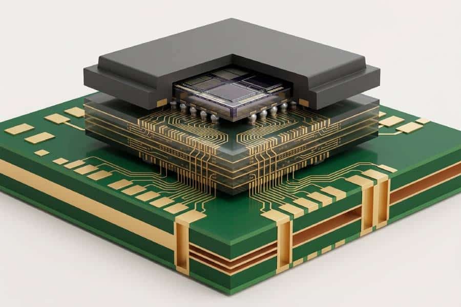
Internally, an IC substrate typically consists of multiple copper layers connected through microvias, buried vias, and sometimes stacked via structures. The build‑up process allows engineers to place thin dielectric layers and fine copper features close to the die, which helps control impedance, reduce parasitics, and support high‑speed signal routing. The stack‑up is carefully designed so that high‑speed signals, power planes, and ground references are arranged to support signal integrity and power integrity within the package.
Reliability requirements also influence how IC substrate materials and structures are chosen. The combination of resin system, glass transition temperature (Tg), coefficient of thermal expansion (CTE), copper thickness, and via construction must be able to withstand repeated thermal cycling, solder reflow, and mechanical stresses without cracking, warping, or delamination near the die interface. As a result, IC substrate manufacturers invest significant effort in material qualification, stack‑up optimization, and process control to ensure that the substrate can maintain stable performance over the full lifetime of the packaged device.
Types of IC Substrates and Package Styles
IC substrates can be classified in several ways, but one of the most practical approaches is to look at the package styles they support. Different package types place different demands on routing density, I/O count, thermal performance, and assembly methods, so the substrate structure must be tailored accordingly.
One of the most widely used package styles is the ball grid array (BGA), which relies on an IC substrate with an array of solder balls on the bottom side. BGA IC substrates are designed to fan out the chip’s I/O to a solder ball pattern that can be mounted on the PCB, while controlling warpage, solder joint reliability, and electrical performance. These substrates are common in processors, networking devices, automotive controllers, and many other high‑pin‑count applications where robust board‑level interconnection is required.
Chip‑scale package (CSP) substrates are used when designers need to keep the overall package footprint very close to the size of the die itself. CSP IC substrates typically support fine‑pitch routing and compact ball or lead patterns, making them suitable for smartphones, wearables, and other space‑constrained consumer electronics. In these applications, the substrate must balance miniaturization with manufacturability and reliability, ensuring stable performance despite the small package size.
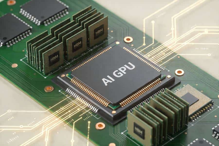
Flip‑chip (FC) substrates support packages where the die is mounted face‑down on the substrate, using an array of solder bumps instead of traditional wire bonds. FC IC substrates must handle very fine bump pitches, high I/O counts, and short interconnect paths that enable higher speeds and better electrical performance. These substrates are widely used in high‑performance computing, AI accelerators, advanced networking devices, and other applications where signal integrity, power distribution, and thermal management are especially critical.
In addition to classifying IC substrates by package style, they can also be distinguished by rigid and flexible constructions. Rigid IC substrates are built on stable laminate or core materials and are suitable for most high‑performance semiconductor packages. Flexible or semi‑flexible IC substrates, which incorporate flexible dielectric layers or constructions, are used in designs that need tighter bending radii, reduced thickness, or special form factors—such as foldable devices or compact modules with 3D stacking requirements.
By understanding the different substrate types and package styles—BGA, CSP, FC, rigid, and flexible—engineers can better match IC substrate technology to the electrical, mechanical, and size constraints of their projects. This alignment is essential for achieving reliable assembly, stable field performance, and efficient manufacturing across a wide range of modern electronic products.
Key Applications of IC Substrates in Modern Electronics
Because IC substrates sit directly under the chip and control how signals, power, and heat move in and out of the package, they appear in many of the most demanding electronic applications today. Wherever designers need compact form factors, high I/O density, and stable high‑speed performance, IC substrate technology is likely to be involved.
In the semiconductor and high‑performance computing space, IC substrates are used in processors, AI accelerators, graphics chips, networking ASICs, and memory devices. These packages often require fine‑pitch flip‑chip connections, dense routing, and carefully controlled impedance to support very high data rates and low latency. The substrate becomes a critical part of the signal and power delivery path, influencing overall system performance.
Telecommunications and networking equipment, including 5G base stations, RF front‑end modules, and high‑speed switches or routers, also rely heavily on IC substrates. In these systems, low loss, stable impedance, and tight process control are necessary to maintain signal integrity at high frequencies. Substrate material selection and stack‑up design play a major role in meeting these RF and high‑speed digital requirements.
Automotive electronics is another fast‑growing application area for IC substrate technology. Advanced driver‑assistance systems (ADAS), electric vehicle control units, in‑vehicle networking, and sensor modules all require reliable, compact, and thermally robust packages. IC substrates in this field must withstand wide temperature ranges, vibration, and long service lifetimes, so reliability and material robustness are especially important.
In consumer electronics, IC substrates enable the thin, light, and compact designs seen in smartphones, tablets, wearables, and IoT devices. Chip‑scale and other miniaturized packages help manufacturers reduce product thickness, increase functional density, and balance performance with battery life. Here, IC substrates support both mechanical integration and the high‑speed interfaces required for modern user experiences.
Medical and industrial systems also benefit from IC substrates where precision, reliability, and long‑term stability are important. Diagnostic equipment, imaging systems, monitoring devices, and industrial control modules often use advanced packages that must operate reliably in controlled or harsh environments over many years. For these products, well‑designed IC substrates contribute to consistent performance, reduced failure rates, and more compact overall system designs.
Key Benefits of IC Substrates in Advanced Packaging
When designers choose to use an IC substrate instead of relying only on traditional PCB technology, they are usually targeting specific performance, integration, or reliability benefits. IC substrates enable packaging solutions that would be difficult or impossible to achieve with system‑level boards alone.
One of the most important advantages is support for higher integration and I/O density. Fine line/space routing, microvias, and build‑up structures allow IC substrates to fan out thousands of I/O connections within a very small footprint, enabling advanced BGA, CSP, and flip‑chip packages. This helps system designers pack more functionality into limited board area and push the limits of performance and miniaturization.
IC substrates also contribute to better electrical performance, especially in high‑speed and high‑frequency designs. Carefully engineered stack‑ups, controlled impedance traces, and short interconnect paths between the die and the substrate help maintain signal integrity and power integrity at the package level. For many AI, networking, and 5G applications, the behavior of the IC substrate has a direct influence on eye diagrams, jitter, loss, and overall system timing margins.
Thermal and mechanical reliability is another key benefit. Because IC substrates sit directly under the chip, their materials and construction help manage heat flow away from local hot spots and support the package during thermal cycling and mechanical loading. The right choice of resin system, copper thickness, and via structure can reduce warpage, limit stress at interconnects, and improve long‑term durability in demanding environments such as automotive and industrial applications.
Finally, IC substrates enable more advanced system architectures and packaging strategies, such as multi‑chip modules, 2.5D/3D integration, and high‑bandwidth interfaces between dies. By providing a dense, high‑performance interconnect platform at the package level, they give engineers an additional design domain—between the chip and the PCB—where signal, power, and thermal behavior can be optimized. This flexibility is becoming increasingly important as modern electronic systems push the limits of speed, power, and functional integration.
IC Substrates and the Future of Advanced Packaging
As electronic systems continue to push for higher performance, lower power, and more functionality in smaller spaces, IC substrates are becoming even more central to advanced packaging strategies. Technologies such as 2.5D integration, 3D ICs, chiplet architectures, and system‑in‑package (SiP) all rely on high‑density interconnect platforms that sit between individual dies and the rest of the system. In many of these designs, the IC substrate effectively becomes a miniature high‑performance circuit board dedicated to managing die‑to‑die and die‑to‑board connections.
Material and structural innovations are also accelerating. Beyond traditional BT and ABF substrates, engineers are exploring glass core substrates, advanced ceramic solutions, and hybrid constructions to support higher frequencies, lower loss, and tighter dimensional control. These developments are particularly relevant for AI accelerators, 5G infrastructure, high‑performance computing, and automotive systems, where signal integrity, thermal behavior, and long‑term reliability must all be carefully managed at the package level.
At the same time, closer co‑design between chips, IC substrates, and system PCBs is becoming more common. Instead of treating the package as a simple carrier, many teams now view the IC substrate as a critical part of the overall electrical and mechanical design that must be optimized together with the silicon and the board. This approach helps unlock better performance and more robust products, but it also increases the importance of choosing manufacturing partners who understand both the design and production aspects of advanced IC substrates.
For engineers and sourcing teams working on next‑generation products, understanding what an IC substrate is—and how materials, structures, and package styles affect performance—has become a key part of the design process. If you are evaluating IC substrate options or looking for support with substrate manufacturing, it can be helpful to work with a supplier that offers both technical guidance and production capability across prototype and volume builds, such as a dedicated IC substrate manufacturing service in China.