Table of Contents
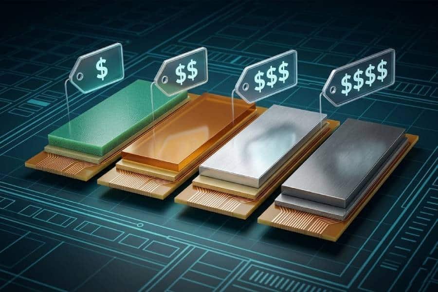
For many hardware teams, the question “How many layers should this PCB have?” quickly turns into “How much more is that going to cost me?”. Moving from a simple 2‑layer board to 4, 6, 8, or even 10+ layers does increase manufacturing cost, but the way that cost scales is more nuanced than “every extra layer doubles the price.” Each step up in layer count changes the stackup, materials, lamination cycles, drilling, registration, and testing requirements—and beyond a certain point, yield and panel utilization can matter as much as the raw number of layers.
In this article, we will look at why layer count is such a powerful driver of PCB manufacturing cost and then walk through the typical trends from 2‑layer to high‑layer‑count boards. You will see what usually happens to cost when you go from 2 to 4 layers (often the biggest “jump”), how 4‑, 6‑, and 8‑layer designs behave in terms of price and trade‑offs, and what changes again when you cross into 10+ layers where yield and size constraints dominate. Along the way, we will highlight other interacting cost drivers—board size, materials, copper thickness, via structures—and share a practical framework for choosing a layer count that supports your routing and signal‑integrity needs without overspending on unnecessary complexity. Finally, we will discuss how a multilayer PCB manufacturer like JHYPCB can help you tune stackup and layer count to hit a better balance between performance and manufacturing cost on your next design.
Why Layer Count Drives PCB Cost
It is no surprise that a 10‑layer board costs more than a 2‑layer board, but the reasons go far beyond “more copper.” Every additional pair of layers adds material, process steps, and risk, and those factors compound as you move up the layer‑count ladder. Understanding these mechanics makes it much easier to predict how a change in layer count will ripple through your manufacturing quote.
More Copper and Dielectric Material
As you increase the number of layers, you add more copper foils and dielectric materials (cores and prepregs) to the stackup. Each additional pair of layers requires extra core or prepreg sheets, copper, and resin, so the raw material cost per panel goes up, especially if you also specify heavier copper or specialty laminates. Higher layer counts can also require tighter control of thickness and dielectric constants, which often means using more advanced—and more expensive—materials than basic FR‑4.
Additional Lamination, Drilling, and Registration Steps
Layer count also drives process complexity. A 2‑layer board can often be built with a single lamination, while 4‑, 6‑, and 8‑layer boards require stacked inner layers to be imaged, etched, and then laminated together under heat and pressure. As you move into higher layer counts or HDI designs, you may introduce sequential lamination cycles, controlled registration between multiple inner stacks, and more drilling passes for through‑holes and microvias. Each extra cycle consumes machine time, tooling, and energy, which shows up directly in manufacturing cost.
Higher Yield Risk and Tighter Process Windows
As stackups become thicker and more complex, the tolerance window for each process step narrows. Inner‑layer registration, lamination pressure and temperature profiles, hole wall quality, and plating uniformity all become more critical to achieving acceptable yield. Any misalignment, void, delamination, or distortion is more likely to cause scrap on a high‑layer‑count panel than on a simple 2‑layer board, simply because there are more layers and interfaces where something can go wrong. To maintain reliable yields, manufacturers must invest in better equipment, tighter process control, and more inspection, and those investments are reflected in the price of complex multilayer builds.
More Complex Testing and Handling
Finally, higher layer counts often require more extensive testing and more careful handling. With more nets, buried structures, and critical impedance paths, 100% electrical test becomes a must rather than an option, and test fixtures or flying‑probe time add to the overall cost of each panel. Thicker, heavier, and more delicate stacks can also demand stricter handling procedures, additional baking, and more controlled packaging to avoid damage in transit, which adds small but real increments to the total manufacturing cost.
From 2-Layer to 4-Layer: The First Big Jump
The cost step from a 2‑layer PCB to a 4‑layer PCB is often the most noticeable jump you will see when increasing layer count. Across many manufacturers, it is common to see a 4‑layer version of the same design priced roughly around one‑and‑a‑third to one‑and‑a‑half times the cost of a comparable 2‑layer board, depending on size, volume, materials, and design rules. The reason is that 4 layers are not just “two more copper layers”—they introduce inner layers, a laminated stack, tighter process control, and more opportunities for yield loss compared with a simple 2‑layer build.
What Changes Technically Between 2 Layers and 4 Layers
A 2‑layer board typically consists of a single core with copper on both sides, processed in one imaging/etching cycle and one lamination step. When you move to 4 layers, you now have two inner layers that must be patterned, inspected, and then laminated together with prepreg and outer copper foils to form a single stack. This adds extra imaging, etching, inspection, lamination, and registration requirements, and it often calls for more precise control of layer alignment and thickness than a basic 2‑layer build.
Why 4-Layer Boards Often Cost Significantly More
These additional materials and process steps show up directly in the quote. You pay for extra copper foils and dielectric layers, more time on imaging and lamination equipment, and a tighter process window that requires better control and more inspection. Because there are now more layers and interfaces where defects can occur, the potential for scrap is higher, so manufacturers factor yield risk into pricing as well. The net effect is that, for a given board size and design complexity, a 4‑layer version is typically substantially more expensive than its 2‑layer counterpart, even before you add any extra features like controlled impedance or HDI.
When 4 Layers Can Actually Save Overall Project Cost
The story, however, is not only about the fabrication quote. Moving from 2 to 4 layers often allows you to shrink board size, simplify routing, improve signal integrity with dedicated planes, and reduce the number of design spins needed to reach a stable layout. For dense digital designs, mixed‑signal boards, or products where enclosure size is constrained, a 4‑layer stackup can reduce debugging time, EMI issues, and layout compromises enough that the total project cost (engineering hours, re‑spins, prototypes) ends up lower than forcing everything onto 2 layers. In other words, while the manufacturing cost per board goes up, the overall cost of getting a reliable design into production can actually go down if 4 layers let the design “breathe.”
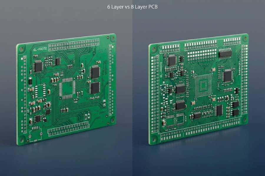
4-Layer to 6- and 8-Layer Boards: Balancing Density and Budget
Once you move beyond 4 layers, the way cost scales with layer count starts to feel a bit different. You are already in the realm of laminated multilayer stacks, so adding more layers usually means extending an existing process rather than introducing inner layers for the first time. In practice, many designers see that going from 4 to 6 layers and then to 8 layers increases cost noticeably, but often in smaller steps than the initial 2‑to‑4‑layer jump, with the exact increment depending heavily on stackup, materials, and fabricator capabilities.
How Cost Typically Evolves from 4 to 6 to 8 Layers
Adding layers on top of a 4‑layer stack means more inner‑layer imaging and etching, a thicker laminate stack, and often additional drilling and plating effort. A 6‑layer board usually adds at least one more pair of signal or plane layers, and an 8‑layer board adds another, so material and process time increase with each step. Many manufacturers report that each extra pair of layers in this range can push cost up by another significant but somewhat smaller fraction compared with the initial 2‑to‑4‑layer jump, especially if design rules and materials remain similar. The exact curve is highly dependent on your board size, panel utilization, copper weights, and whether you introduce additional complexity like blind or buried vias.
When 6 Layers Make Sense
A 6‑layer stack is a common sweet spot for many digital and mixed‑signal designs. It allows you to dedicate more layers to solid reference planes and cleaner routing—for example, using two inner planes for power and ground plus four signal layers to separate high‑speed paths and reduce crosstalk. Compared with 4 layers, the extra layers can reduce the need for aggressive via usage, complex fan‑outs, and risky compromises in return paths, which can shorten layout time and improve signal integrity. If your design is too dense or too fast to be comfortably handled in 4 layers but does not yet demand extensive segmentation or isolation, moving to 6 layers is often the most balanced way to buy routing freedom without jumping straight to a more expensive 8‑layer stack.
When 8 Layers Are Justified
An 8‑layer board tends to come into play when you need even more structure in your stackup—either for very dense routing, stricter EMC performance, or complex power distribution. For example, high‑pin‑count FPGAs or SoCs with multiple high‑speed interfaces, or systems with many isolated power domains, often benefit from 8‑layer stacks that can alternate signal and plane layers to tightly control impedance and reduce coupling. The extra layers give you room to separate noisy and sensitive nets, provide multiple clean reference planes, and route dense BGA breakouts without resorting to extreme design rules. While the fabrication cost of an 8‑layer board is higher than a comparable 6‑layer one, in these scenarios it can be more cost‑effective overall than trying to force a complex design into 6 layers and paying the price in redesigns, EMI fixes, or field issues.
Watching for Diminishing Returns
Between 4, 6, and 8 layers, each increase buys you more routing freedom and signal‑integrity headroom, but also pushes up fabrication cost and complexity. The key is to recognize where you hit diminishing returns—where adding yet another pair of layers does not significantly simplify the layout or improve performance, but still carries a meaningful cost premium. Working with your PCB manufacturer to review your proposed stackup and routing constraints can help you decide whether a given design truly needs 8 layers, or whether a well‑planned 6‑layer stack will achieve the same goals at a lower manufacturing cost.
10+ Layer and High-Layer-Count Boards: Where Cost Scales Differently
When you move into 10‑layer and higher‑layer‑count boards, the cost behavior changes again. At this point you are no longer just “adding a couple more layers” to a conventional stack; you are working with thick, complex constructions where yield, mechanical stability, and size constraints start to dominate the cost picture. Two 12‑layer designs with the same net count and rules can have very different costs if one pushes panel limits, uses exotic materials, or requires multiple sequential lamination cycles.
Yield and Process Complexity Become the Main Drivers
In high‑layer‑count stacks, every process variable—inner‑layer registration, lamination pressure/temperature, drill accuracy, plating uniformity—has less margin for error. With many layers and interfaces, slight misalignments, resin voids, or warpage can cause an entire panel of boards to be scrapped. Manufacturers therefore treat high‑layer‑count builds as higher‑risk jobs: they may require more detailed engineering review, tighter process controls, additional in‑process inspections, and sometimes lower panel loading to keep yields acceptable. All of this time, attention, and risk is reflected in the price, often more strongly than the raw incremental cost of the extra copper and dielectric.
Board Size and Panel Utilization Matter Even More
Layer count and board size interact strongly at the high end. As layer count increases, the maximum practically achievable board size can shrink because thicker stacks are harder to keep flat and stable across large areas. To maintain yield, manufacturers may limit the usable area per panel, increase border margins, or reduce the number of boards they place on each panel, which drives up the cost per unit. Designs that push both high layer count and large dimensions at the same time therefore tend to see disproportionately higher prices compared with smaller boards of the same layer count, simply because panel utilization and risk are worse.
Non-Linear Cost Scaling Beyond a Certain Layer Count
Because of these effects, the cost curve for 10+ layer boards is rarely linear. You might see that going from, say, 10 to 12 layers on a modest‑size board adds a relatively predictable increment, but that pushing the same design to 14 or 16 layers or increasing its dimensions dramatically changes its risk profile and price. In other words, once you are in high‑layer‑count territory, the incremental cost of “two more layers” can swing widely depending on how close you are to a particular fabricator’s process and panel limits. This is why it becomes especially important to involve your PCB manufacturer early when planning high‑layer‑count designs—they can flag combinations of layer count, size, and features that will be disproportionately expensive or difficult to build reliably.
Other Cost Drivers That Interact with Layer Count
Layer count is a major cost driver, but it never acts alone. Board size, material choices, via strategy, and design rules all interact with how expensive a given layer count will be, which is why two 6‑layer designs can have very different prices. Keeping these factors in mind helps you avoid blaming layer count for cost increases that actually come from other design decisions.
Board Size and Panel Utilization
Board outline and panelization have a direct impact on cost per unit. Larger boards consume more material and can reduce the number of pieces that fit on a standard manufacturing panel, which raises the cost per board even if the layer count stays the same. Unusual shapes, large keep‑outs, or small gaps between boards can also hurt panel utilization and increase scrap, further pushing up cost. For a given layer count, optimizing your outline and panelization with your fabricator is one of the most effective ways to control manufacturing cost.
Materials and Copper Thickness
Material selection can amplify or moderate the cost impact of layer count. Standard FR‑4 at typical Tg and moderate copper weights is generally the most cost‑effective choice; moving to high‑Tg, high‑speed, RF, or halogen‑free laminates adds a premium that multiplies with every added layer. Similarly, specifying heavy copper on inner or outer layers increases both material usage and plating time, which becomes more expensive as the number of copper layers grows. A 6‑layer board built entirely with high‑speed materials and heavy copper can easily cost more than an 8‑layer board using standard laminates and moderate copper weights.
Via Structures and Density
Your via strategy is another major lever. Simple through‑hole vias are the most economical, but as you add more layers and denser components, you may be tempted to adopt blind, buried, or microvia structures, or via‑in‑pad fan‑outs under BGAs. These advanced via types usually require extra drilling, laser equipment, sequential lamination, and more careful plating, all of which add process steps and yield risk on top of whatever the layer count already costs. Choosing a stackup that supports efficient fan‑outs with mostly through‑hole vias can therefore be a powerful way to keep both layer count and via complexity under control.
Trace/Space and Tolerance Requirements
Finally, your minimum trace/space and tolerance requirements can magnify cost differences between layer counts. Very fine features demand tighter process control, more advanced imaging, and more inspection, which all become harder and more expensive as you stack up more layers. A design that uses conservative line widths and clearances may scale relatively gently in cost as you go from 4 to 6 to 8 layers, while an aggressively dense design with fine BGA pitches and tight clearances will see much steeper cost increases for the same layer steps. In many cases, relaxing design rules slightly or re‑thinking component placement can avoid unnecessary layer count increases and keep you in a more economical manufacturing window.
How to Choose the “Right” Layer Count for Cost and Performance
Selecting a layer count is ultimately an engineering trade‑off, not a purely financial one. The goal is to choose the lowest layer count that still gives you clean routing, acceptable signal and power integrity, and manageable risk—without artificially forcing the design into a stackup that will cost more in re‑spins and debugging later. A structured way to approach this decision makes it much easier to justify why you stopped at 4, moved to 6, or pushed to 8 or more layers.
Start from Routing, Signal Integrity, and EMI Needs
Begin by mapping the electrical and layout requirements of your design. Consider net density, BGA pin counts, critical high‑speed interfaces, return path quality, and any EMC or safety constraints that demand solid reference planes or careful segregation. Ask whether a 2‑layer or 4‑layer board can realistically provide continuous planes and clean routing for your highest‑risk signals without resorting to extreme design rules; if not, a 6‑ or 8‑layer stackup may actually reduce total project risk. Let these technical needs set an initial “candidate range” for layer counts rather than starting from a target number and trying to force the design to fit.
Use Common Layer “Steps” as Checkpoints
Most designs naturally cluster around a few common layer counts—2, 4, 6, 8, and then 10+ for more complex systems. For each of these checkpoints, sketch a plausible stackup: how many signal layers, how many planes, and how you would assign high‑speed nets, sensitive analog sections, and noisy power or digital regions. If you find that forcing everything into 4 layers drives you to very tight design rules, convoluted return paths, or repeated via‑stitching tricks, that is a strong hint that 6 layers may be the “right” choice despite the higher fabrication cost. Conversely, if an 8‑layer concept does not clearly simplify routing or improve integrity compared with 6 layers, you may be paying for extra complexity without getting enough benefit back.
Factor in Size, Materials, and Via Strategy
Once you have one or two plausible layer counts, overlay the other major cost drivers. Check whether board size and panelization can be optimized at each layer count, whether you truly need high‑speed or special laminates, and how your via strategy will change (through‑hole only versus blind/buried or via‑in‑pad). A design that fits on a smaller outline in 6 layers with mostly through‑hole vias might cost less overall than a 4‑layer version that forces a larger board and more aggressive features. By looking at layer count together with size, materials, and vias, you avoid misleading comparisons where one option appears cheaper only because hidden costs have been ignored.
Validate Options with Your PCB Manufacturer
Finally, bring your shortlisted stackups to your PCB manufacturer and ask for feedback. A good multilayer fabricator can quickly tell you which layer counts and stackups align best with their process sweet spots, panel sizes, and yield history. They may suggest minor stackup changes, different copper weights, or alternative via structures that keep you within the same layer count while reducing cost and risk—or, in some cases, recommend adding a layer to avoid design choices that are disproportionately expensive to manufacture. Using real quotes and DFM feedback to compare 4‑, 6‑, 8‑, and 10+‑layer options turns layer count selection from a guess into a data‑backed decision.
How a Multilayer PCB Manufacturer Like JHYPCB Helps Optimize Cost vs Layer Count
A multilayer PCB manufacturer that regularly builds 4‑, 6‑, 8‑ and high‑layer‑count boards can add a lot of value to your layer‑count decision, beyond simply quoting a price. By combining process experience, cost data, and DFM feedback, they can help you choose stackups and layer counts that fit both your technical needs and their most efficient manufacturing windows. JHYPCB positions itself in exactly this role for overseas customers, focusing on cost‑effective multilayer fabrication with engineering support.
Stackup and Layer-Count Recommendations
JHYPCB emphasizes strong front‑end engineering and DFM review as part of its multilayer service, which includes evaluating your proposed stackup and suggesting alternatives when they see cost or yield risks. For example, they can point out when a design could safely move from 8 to 6 layers by re‑allocating planes and adjusting routing strategy, or when adding a layer might actually allow more economical routing and via structures. Because they see many designs across different layer counts and technologies, they can compare your options against real manufacturing data instead of relying on generic rules of thumb.
Panel Optimization, Materials, and Via Strategy
A manufacturer like JHYPCB also has visibility into how your design will sit on production panels and which combinations of materials and via structures are most efficient to build. They can recommend outline or panelization changes to improve panel utilization, suggest when standard FR‑4 is sufficient versus when high‑speed or special materials are truly required, and advise on whether blind or buried vias are justified for your chosen layer count. In many cases, small adjustments in board size, stackup, and via strategy—guided by the fabricator—can reduce cost enough that you can afford an extra layer where it genuinely simplifies the design, or safely drop a layer without creating hidden manufacturing penalties.
Supporting Prototypes Through to Volume
Because JHYPCB targets both quick‑turn multilayer prototypes and small‑to‑medium production runs, they can help you validate layer‑count decisions early and then carry those decisions into volume without a disruptive transfer. You can start with a 4‑, 6‑, or 8‑layer prototype, review DFM feedback and yield behavior, and then lock in a stackup that scales well for cost and reliability as orders grow. This fits naturally with a dual‑sourcing model: you might prototype locally when speed or on‑site collaboration is critical, then engage JHYPCB to co‑evaluate layer count and stackup for ongoing multilayer builds where overseas fabrication can deliver better cost or capacity.