Table of Contents
As AI accelerators and high‑performance computing (HPC) processors grow larger, faster, and more power‑hungry, IC substrates for AI and high‑performance computing have become a critical part of the system design. They must route thousands of high‑speed signals, deliver clean power to massive dies or multi‑die packages, and help extract heat efficiently—all within very tight electrical and mechanical constraints. This article looks at how AI/HPC architectures drive IC substrate requirements and examines the key design and material considerations engineers and sourcing teams need to evaluate.
Why AI and HPC Push IC Substrates to the Limit
Workload and architecture trends in AI/HPC
AI training, large‑scale inference, and high‑performance computing (HPC) simulations all demand enormous parallel compute, very high memory bandwidth, and tight latency budgets. To meet these requirements, AI and HPC chips have grown into large dies or multi‑die packages with wide internal data paths and many high‑speed external interfaces. Architectures now routinely combine massive arrays of compute cores with on‑package or closely coupled memory, creating very dense interconnect requirements near the processor. As a result, the IC substrate must support far more I/O, higher signaling speeds, and higher power densities than in traditional consumer or industrial devices.
What makes AI/HPC packages different from “normal” devices
Several characteristics distinguish AI/HPC packages from more conventional IC packages. First, die sizes often approach or exceed reticle limits, and multi‑die or chiplet‑based configurations bring multiple large dies and HBM stacks together on a single substrate. This drives extremely high bump counts, fine bump pitches, and wide buses between compute and memory, which in turn require very dense routing, carefully planned stack‑ups, and advanced materials in the IC substrate. Second, AI/HPC devices typically operate at high power levels and sustained utilization, so the substrate must handle intense thermal loads and repeated thermal cycling while maintaining warpage control and interconnect reliability. Finally, these systems often need long product lifetimes and predictable behavior under data‑center or edge‑compute conditions, which raises the bar for substrate material selection, design margins, and manufacturing process stability.
AI and HPC Package Architectures and Their Impact on Substrates
Large monolithic dies and reticle‑limited AI/HPC processors
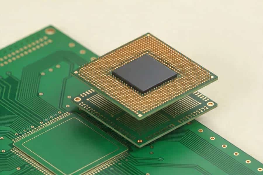
Many AI and HPC processors are implemented as very large monolithic dies that push up against photolithography reticle limits, resulting in packages with extremely high bump counts and tight bump pitches. The IC substrate for such devices must fan out thousands of power, ground, and high‑speed signal connections within a limited footprint, which demands very fine line/space, dense microvia structures, and carefully engineered stack‑ups. Substrate warpage and mechanical stability become critical, because even small distortions can affect assembly yields, bump reliability, and board‑level solder joint quality under these large die footprints.
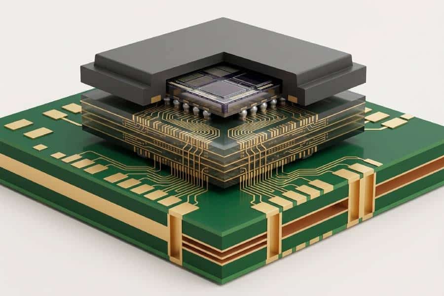
Multi‑die, chiplet, and 2.5D/3D integration (HBM, interposers)
To overcome reticle and yield limitations, many AI/HPC designs now use multi‑die or chiplet architectures, often combined with high‑bandwidth memory (HBM) or other stacked memory solutions. In 2.5D and 3D configurations, an IC substrate may work together with a silicon or glass interposer, or directly host multiple dies and HBM stacks, creating a dense web of die‑to‑die and die‑to‑memory connections that all must be routed through the package. This increases requirements on substrate layer count, via strategies, and routing topology, as designers must balance short, low‑loss interconnects with manufacturable via stacks and robust power distribution.
High‑bandwidth memory interfaces and wide IO buses
High‑bandwidth memory interfaces and other wide I/O buses used in AI and HPC systems put exceptional pressure on IC substrate design. HBM links, for example, involve hundreds or thousands of parallel data lines and associated clocks and control signals that must be length‑matched, impedance‑controlled, and routed with tight skew and crosstalk constraints between the processor and memory stacks. These requirements drive complex layer partitioning, dense escape routing, and precise reference plane planning within the substrate, often pushing designers toward ABF‑based build‑up structures or other advanced material systems that can support such density and performance.
Key Design Considerations for AI/HPC IC Substrates
Signal integrity for ultra‑high‑speed links
AI and HPC substrates must support a mix of very high‑speed serial links, wide memory buses, and dense on‑package interconnects, all of which are sensitive to loss, reflections, and crosstalk. Designers need to treat the IC substrate as part of the end‑to‑end channel, optimizing trace geometry, dielectric properties, reference planes, and via transitions to meet eye‑diagram and jitter requirements at target data rates. Careful length matching, skew control, and breakout strategies for HBM and SerDes interfaces are essential to avoid signal‑integrity issues that cannot be fixed later at the PCB level.
Power delivery network (PDN) and low‑noise power to the die
Power delivery is equally demanding in AI/HPC packages because large dies or multi‑die assemblies draw high currents on multiple voltage rails with fast load transients. The IC substrate must integrate robust power and ground planes, low‑impedance via networks, and effective decoupling strategies to keep voltage ripple and noise within tight limits at the die bumps. PDN design on the substrate has to be coordinated with on‑package capacitors, die‑level power grids, and the board‑level PDN so that impedance targets are met across the relevant frequency range.
Thermal path and heat spreading
High‑power AI accelerators and HPC processors can dissipate hundreds of watts, making thermal design a core substrate concern. The substrate contributes to heat removal by providing copper planes and thermal paths from the die into heat spreaders, lids, or direct‑attached cooling structures, and by supporting thermal vias and connections down into the PCB or system‑level cooling solution. Material choices, copper distribution, and mechanical stack‑up all influence junction‑to‑case and junction‑to‑board thermal resistance, as well as warpage behavior during temperature changes.
Mechanical and reliability constraints under AI/HPC loads
AI/HPC systems often operate at high utilization and elevated temperatures over long periods, which increases mechanical and reliability demands on IC substrates. Repeated thermal cycling, large die sizes, and complex multi‑die stacks can amplify stresses at bumps, microvias, and material interfaces, especially where CTE mismatches exist between silicon, substrate materials, and any interposers or lids. To achieve acceptable lifetimes and qualification results, substrate designs must consider material selection (Tg, CTE, modulus), stack‑up symmetry, via reliability, and warpage control from the earliest stages of AI/HPC package development.
Material Choices for AI/HPC IC Substrates
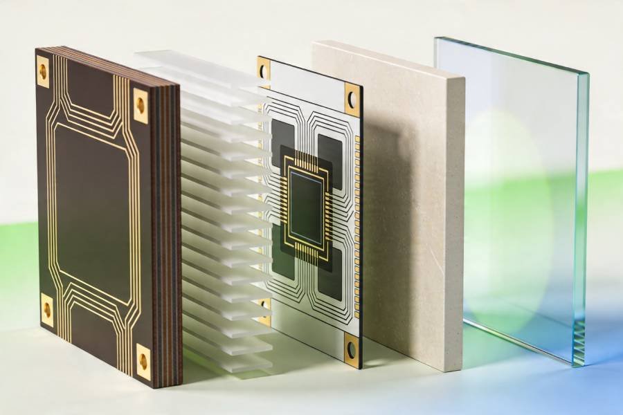
ABF build‑up substrates for high‑end AI and HPC chips
Ajinomoto Build‑up Film (ABF) has become the dominant material system for many high‑end AI and HPC IC substrates because it supports extremely fine lines, small microvias, and multi‑layer build‑up structures close to the die. Its controlled dielectric properties and thin, uniform layers help designers meet tight impedance and loss budgets for high‑speed SerDes links and wide HBM interfaces. As AI and HPC packages grow in I/O count and bandwidth, ABF substrates offer the density and electrical performance needed to route thousands of signals within a constrained footprint.
BT resin substrates in performance‑cost balanced designs
BT resin substrates are widely used in performance‑oriented designs that still need to balance cost and manufacturability, such as mid‑range accelerators, networking equipment, and some AI/HPC companion devices. BT materials provide good thermal stability, decent dielectric performance, and robust reliability characteristics, making them suitable for many high‑speed and high‑power applications that do not require the absolute highest density achievable with ABF. In AI/HPC systems, BT‑based substrates can be a practical choice for control, I/O, or less demanding compute devices that still operate near large processors but have more moderate routing and bandwidth needs.
Ceramic substrates for power and harsh environments
Ceramic IC substrates, such as those based on alumina or aluminum nitride, are particularly attractive for power modules and harsh‑environment electronics that sit alongside AI and HPC compute engines. Their high thermal conductivity, high‑temperature stability, and mechanical strength make them well suited to manage the heat and environmental stress associated with power conversion and distribution in high‑density computing systems. While their routing density and feature sizes are generally less aggressive than ABF or advanced organic systems, ceramics can offload thermal and reliability challenges from the main compute substrate by hosting high‑power or high‑voltage functions on separate, more robust modules.
Glass and glass‑core substrates for next‑generation AI/HPC
Glass‑core and glass‑based IC substrates are emerging as promising options for next‑generation AI and HPC packaging, especially where very high frequencies, ultra‑wide interfaces, or very large package footprints are involved. Glass offers low and stable dielectric constant, low loss, excellent dimensional stability, and low in‑plane CTE, which are beneficial for high‑speed signaling and precise registration across large substrates or panels. For advanced AI/HPC architectures that combine many chiplets and memory stacks, glass substrates may help enable denser, more uniform interconnect platforms, though their processing, fragility, and cost considerations mean they are still mostly used in leading‑edge or exploratory designs today.
Stack‑up and Routing Strategies for AI/HPC IC Substrates
Layer partitioning and stack‑up planning
AI and HPC IC substrates typically use high layer counts, with a clear vertical partition between high‑speed signal layers, continuous reference planes, and thicker power/ground layers to balance signal integrity and manufacturability. A common pattern is to place multiple fine‑line high‑speed routing layers with tightly coupled reference planes close to the die, and reserve mid and far‑from‑die layers for coarse power distribution and lower‑speed control or management signals.
Via structures and escape routing
For high I/O‑count AI/HPC packages, microvias, buried vias, and via‑in‑pad structures are widely used to escape dense bump arrays efficiently while maintaining signal quality. Stacked or staggered build‑up microvias, sometimes combined with back‑drilled through‑holes, help minimize via stubs, reduce impedance discontinuities, and relieve local routing congestion so that extremely dense interfaces remain routable.
Length and skew control for high‑speed links
Wide HBM buses and multi‑lane SerDes channels require tight length matching and skew control so that all bits or differential lanes arrive within a narrow timing window. Designers rely on serpentine tuning, symmetric via and layer transitions, and consistent dielectric paths to keep intra‑pair and inter‑pair length mismatches within a few mils or less, meeting multi‑GHz timing and jitter budgets for AI/HPC interfaces.
Reference planes and return‑path management
To reduce crosstalk and radiation, high‑speed traces are routed over continuous reference planes and avoid crossing plane splits that would force return current to detour. Dense ground via “fences” or grids are often placed near chiplet edges, routing transitions, and channel corners to provide short, stable return paths and support good power integrity across large AI/HPC substrates.
Design Flow and Co‑Optimization for AI/HPC IC Substrates
System‑to‑package co‑design and early partitioning
AI/HPC designs benefit from a system‑to‑package co‑design flow where chip architects, package engineers, and board designers agree early on I/O partitioning, power rails, and placement of chiplets and HBM stacks. Early co‑planning of bump maps, substrate stack‑up, and board escape regions helps avoid late congestion issues and reduces the number of design spins needed to hit performance and yield targets.
SI/PI co‑simulation as a core sign‑off step
Because AI/HPC links are extremely fast and power‑hungry, modern flows treat signal integrity (SI) and power integrity (PI) as a unified problem rather than two separate checks. Designers use SI/PI co‑simulation to model die bumps, substrate traces and vias, interposers, and the board PDN in one environment, so they can see how switching currents, PDN noise, and channel loss interact before committing to fabrication.Lorem ipsum dolor sit amet, consectetur adipiscing elit. Ut elit tellus, luctus nec ullamcorper mattis, pulvinar dapibus leo.
DRC, DFM, and DFR in substrate layout
Beyond basic design rule checks (DRC), AI/HPC substrates rely on design for manufacturing (DFM) and design for reliability (DFR) rules to keep very fine features manufacturable and robust. DFM rules extend simple spacing/width checks with constraints on aspect ratios, via stacks, solder mask, and assembly clearances, while DFR adds rules aimed at long‑term robustness, such as via redundancy, copper balancing, thermal‑mechanical relief structures, and PDN robustness under stress.
Iteration with substrate vendors and prototyping
Given the tight process windows in advanced organic and glass‑core substrates, close iteration with the fabrication vendor is now a standard part of the AI/HPC design flow. Design teams typically prototype early builds to validate stack‑up, material choices, drill strategies, and fine‑line capability, then refine design rules and models from measured data before ramping to volume production.
Manufacturing Flow for AI/HPC IC Substrates
Core process flow and materials
Advanced IC substrates for AI and HPC typically follow a multilayer build‑up flow that includes core preparation, patterning/etching of copper, build‑up lamination, via drilling, metallization, and final surface finish. ABF or other build‑up films are laminated in multiple cycles on an organic or glass core, then laser‑drilled and copper‑plated to form ultra‑fine redistribution layers capable of routing dense AI/HPC bump maps.
Fine‑line patterning and via drilling
As AI/HPC I/O counts and speeds rise, manufacturers must pattern very fine copper lines and spaces on sometimes uneven topography, which demands high registration accuracy and tight process control. Laser via drilling (often UV) is used to form microvias down to tens of micrometers, and accurate target acquisition is critical so vias land on pads within small tolerances while still maintaining acceptable throughput.
Warpage control during fabrication and assembly
Thicker, larger, and higher‑layer substrates for AI/HPC are especially prone to warpage because of CTE mismatches between resin, glass fiber, copper, and build‑up films. Symmetric stack‑ups, balanced copper distribution, optimized resin content, and careful control of lamination and curing profiles are widely used to keep static and process‑induced warpage within assembly tolerances.
Yield‑critical defects and process windows
Yield in advanced AI/HPC substrates is strongly impacted by small defects such as voids in build‑up films, via drilling defects, fine‑line opens/shorts, and local warpage that prevents proper bump or BGA solder wetting. As package sizes and layer counts grow, even a single critical defect can represent a large percentage loss in yield per panel, so manufacturers invest heavily in high‑resolution inspection, metrology for ABF thickness, and tighter process windows around lamination, drilling, and patterning.
Reliability and Qualification of AI/HPC IC Substrates
Thermal cycling and CTE‑mismatch driven stress
AI/HPC packages see wide temperature swings during operation and qualification, so substrates are qualified with thermal cycling tests that repeatedly cycle between low and high temperatures (for example, around −40 °C to 125 °C). Large CTE mismatches between silicon (around 2–3 ppm/°C) and organic substrates (typically 16–18 ppm/°C) create significant mechanical stress at bumps, microbumps, and interfaces, which can lead to warpage, delamination, and solder joint cracking if not properly managed.
Warpage, dynamic deformation, and failure modes
Warpage is a central reliability concern in large AI/HPC substrates because out‑of‑plane deformation changes with temperature and can concentrate stress in copper pillars, RDLs, and joints. Studies that monitor dynamic warpage during thermal cycling show that larger or thinner packages tend to exhibit higher warpage amplitudes, which correlate with earlier onset of failures such as RDL cracks, bump fatigue, and pad‑cratering at the board interface.
Qualification tests and lifetime evaluation
Reliability qualification for AI/HPC substrates combines multiple stress tests, including thermal cycling, thermal shock, high‑temperature storage, temperature–humidity bias, and board‑level bend or drop, to uncover different failure mechanisms. For large flip‑chip or 2.5D/3D packages, test plans often add specific warpage‑monitoring and assembly‑reflow simulations so that substrate stack‑up and stiffener choices can be tuned to keep deformation and stress within acceptable limits over the product lifetime.
Panel‑Level Packaging and Its Impact on AI/HPC Substrates
Cost and throughput advantages at panel scale
Panel‑level packaging (PLP) processes larger rectangular panels instead of wafers, allowing many more AI/HPC or chiplet packages to be built per pass and improving equipment utilization. By spreading material and process costs over a larger number of units, PLP can reduce per‑unit substrate and packaging costs by a significant margin, which is attractive for data‑center‑class AI accelerators where cost per performance is critical.
Yield, risk concentration, and inspection
At panel scale, a single defect or process excursion can impact many more devices at once, so yield management and inline inspection become even more critical than in wafer‑level flows. Advanced PLP lines use high‑resolution inspection, statistical process control, and predictive yield modeling to control contamination, registration, and warpage across the full panel, enabling very high yields (reported above 99% in some high‑volume PLP operations) even for complex AI/HPC packages.
Implications for AI/HPC substrate design
For AI/HPC devices, PLP pushes substrate designers to consider panel‑compatible formats, more uniform copper distribution, and stack‑ups optimized for both warpage and panel utilization. As panel‑level approaches mature, they are expected to support larger multi‑die and chiplet‑based AI packages, combining cost reductions with the fine‑line and high‑layer‑count capabilities needed for high‑bandwidth memory and advanced die‑to‑die interfaces.
Conclusion: AI/HPC IC Substrates as a Strategic Enabler
AI and HPC workloads are pushing IC substrates from a “back‑end commodity” into a strategic enabler that directly limits or unlocks system performance, power, and cost. Higher I/O density, wider memory interfaces, and multi‑die architectures mean substrates must deliver ultra‑fine routing, tight SI/PI control, strong thermal paths, and robust reliability, often at unprecedented package sizes and power levels.
At the same time, market and technology trends such as chiplet‑based design, HBM‑centric memory architectures, 2.5D/3D stacking, glass‑core substrates, and panel‑level packaging are converging to reshape how AI/HPC substrates are specified and manufactured. Design teams that treat the substrate as a first‑class design object—co‑optimizing die, package, board, and manufacturing early—are best positioned to achieve competitive AI/HPC products in terms of both performance and total cost of ownership.
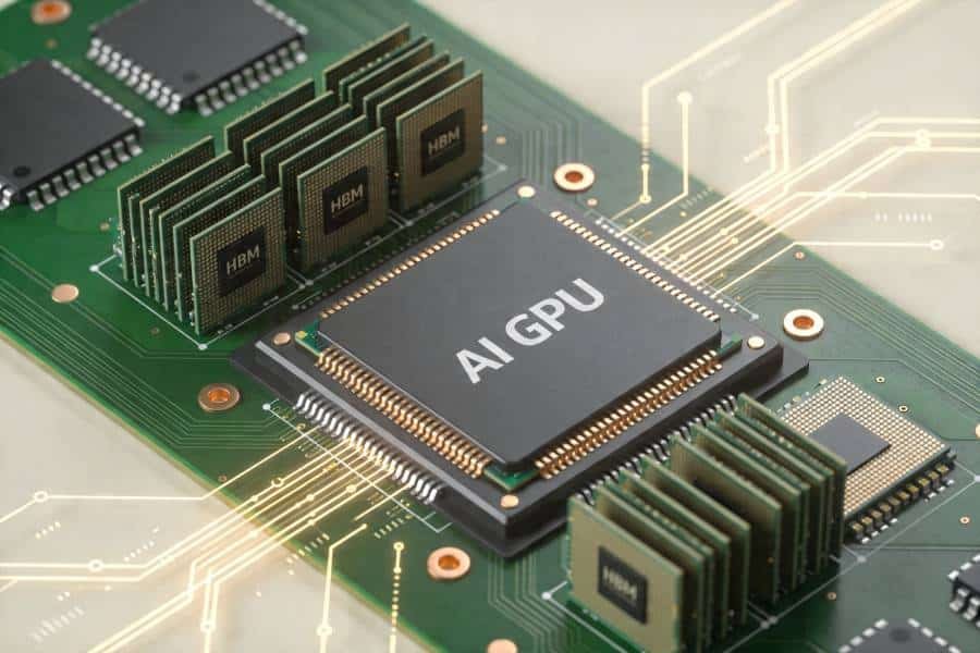
Case Study 1: GPU + HBM Substrate for AI Training
Modern AI training accelerators, such as GPUs with multiple HBM stacks, illustrate the tight coupling between package architecture and substrate design. A typical configuration uses a very large logic die flanked by four to eight HBM stacks, with thousands of wide I/O connections per stack routed through an advanced organic or ABF‑based substrate and, in many cases, a 2.5D interposer.
To support aggregate memory bandwidths in the multi‑terabyte‑per‑second range, the substrate must provide high‑layer‑count build‑ups, ultra‑fine line/space, carefully length‑matched HBM channels, and a low‑impedance PDN, while controlling warpage across a large body size so that all microbumps and BGA balls remain reliable over temperature and lifetime. These packages are often at the forefront of adopting new materials (low‑loss dielectrics, glass‑core candidates) and tighter co‑design flows because even small SI/PI or mechanical issues can limit achievable data‑rate or reduce usable yield.
Case Study 2: Chiplet‑Based AI/HPC Processor Substrates
Chiplet‑based AI/HPC processors disaggregate a monolithic SoC into multiple logic chiplets surrounded by HBM or other memory, all tied together on an advanced substrate or bridge/interposer fabric. The substrate in such systems not only fans out external I/Os but also implements high‑bandwidth die‑to‑die links between chiplets, effectively acting as a high‑speed network‑on‑package.
This architecture increases substrate design complexity: designers must handle many high‑speed chiplet links, more localized power domains, and sometimes mixed‑signal or RF functions, all within a constrained footprint and warpage budget. It also makes co‑optimization with manufacturing vital, because yield now depends on both individual chiplets and the substrate/interposer; panel‑level and glass‑core solutions are being explored to balance cost, warpage, and high‑speed performance for these large, heterogeneous AI/HPC modules.